techmannih/nema34-mounted-stepper-controller
A 48 V USB‑C PD 3.1 EPR NEMA‑34 stepper controller PCB combining STM32/TMC5160 control, external MOSFET motor bridges, protected power and regenerative braking, USB data, telemetry, diagnostics, status LEDs, and buzzer alarms.
- Version
- 0.3.92
- License
- unset
- Stars
- 1
docs/u16-footprint.md
# U16 stocked MCU revision

U16 is **ST STM32G0B1CEU6 / JLCPCB C2829190**, UFQFPN48, GP pinout, 512 KiB flash and 144 KiB SRAM. Do not substitute the `...U6N` alternate pinout or the former LQFP48 device onto this PCB.

The authoritative lands follow [ST DS13560 Rev 6, figures 6 and 46](https://www.st.com/resource/en/datasheet/stm32g0b1cb.pdf): 48 peripheral lands at 0.50 mm pitch, 0.30 × 0.55 mm, with row centres ±3.375 mm, and a 5.60 × 5.60 mm ground land. Pin 1 is bottom-left in this board orientation. The exposed pad is explicitly represented as pin 49 / EP_GND and connected to GND. The first 48 functional pin numbers are unchanged. The new local fanout must pass native DRC and the same-side C44/C45/C46 bypass checks. Moving the MCU lands inward by 0.875 mm extends the existing bypass branches while preserving capacitor and crystal placement. The explicit 3.7 mm placement override covers their new straight-line spacing; the native routed-path limit remains 5 mm.

Four 0.60/0.30 mm ground vias stitch the exposed pad to the ground planes and require filled/capped processing. The 4.60 × 4.60 mm nominal paste aperture is about 67.5% of pad area; the assembler must approve stencil thickness/windowing and inspect QFN soldering. Local DRC checks all four layers around the vias.

The explicit UFQFPN model is associated with C2829190, EasyEDA UUID `16912e571dfb42a9a47b4df7b841ed45`, rotated 90° to match the pin-1 corner. CAD provenance: [JLCEDA/EasyEDA Official Library](https://easyeda.com), [JLCEDA](https://lceda.cn/). A 3D model does not establish solder-joint acceptance.

The firmware target is `stm32g0b1ceu6` / `ARDUINO_GENERIC_G0B1CEUX`. Full flash readback is **524,288 bytes from 0x08000000**. USB, SWD, ADC, SPI and I2C pin assignments remain the GP assignments; motion qualification flags remain false. See [readiness](readiness.md) for physical programming and cold boot.

The crystal escape uses the board's existing 0.09 mm minimum trace/space class through the narrow corner clearance; it stays on F.Cu to the retained crystal route. Other dense sense escapes use 0.10 mm traces. These are logic/ADC paths, not motor-current conductors. Native DRC and the local-copper preservation check cover the exact final geometry; the fabricator must accept the stated 0.09 mm process.
Related Packages
 More from this authortechmannih/schematic-testA PCB with a 6-pin SPI display connector linked to SPI signals, ground, and 3.3V power.
 Similar packageimrishabh18/rp2040-motor-controllerAn RP2040-based NEMA17 stepper-motor controller with USB-C programming and PD motor-power negotiation, DRV8825 dual H-bridge drive, current/temperature telemetry, protected power filtering, status RGB LED, buzzer alarm, and optional magnetic encoder.
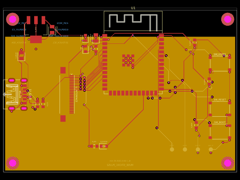 Discover something newShiboSoftwareDev/muse-m5stack-stickc-plus2-replacementA 4-layer ESP32-S3 carrier board with USB-C 5V input, AMS1117 3.3V regulation, buttons, status LED, decoupling passives, and a 24-pin FFC interface for display, touch, audio, or sensor peripherals.