techmannih/nema34-mounted-stepper-controller
A 48 V USB‑C PD 3.1 EPR NEMA‑34 stepper controller PCB combining STM32/TMC5160 control, external MOSFET motor bridges, protected power and regenerative braking, USB data, telemetry, diagnostics, status LEDs, and buzzer alarms.
- Version
- 0.3.92
- License
- unset
- Stars
- 1
docs/manufacturing-acceptance.md
# Manufacturing and mechanical acceptance

**Prepared requirements; supplier and physical acceptance remain pending.** Keep the four existing PCB holes and all unrelated copper; the reviewed U16/U35 ECO and J1/J10 USB edge placement are documented in their respective evidence files. Record the exact release hash, provider, drawing revision, approver/date and evidence for each row. A public capability page confirms an offered process, not acceptance of this board.

| Area | Requirement for this board | Closure record |
|---|---|---|
| PCB/process | 85.9 × 85.9 mm stepped outline, 4 layers, 1.6 mm, **1 oz on every copper layer**, green mask, white silk, **ENIG**, top assembly, electrical test | Accepted fabrication drawing/quote with all parameters, including 0.09 mm trace/space |
| Via-in-pad | **63 locations**, including 40 MOSFET drain-pad vias and four U34 thermal vias and four U16 ground-pad vias; **epoxy filled and copper capped**, minimum finished via drill 0.30 mm | Provider accepts coordinate list and native board; inspect planarity and first-article solder joints |
| USB | 90 Ω differential target, project acceptance ±10%; review USB_DP/DM and USB_DP_CONN/DM_CONN against selected stack-up | Stack-up ID with copper/dielectric thickness and material, field-solver report for actual width/gap/plane geometry, coupon/TDR result and USB test |
| USB receptacles | C3025063 / USB4105-GF-A-060; 0.60 mm shell stakes on 1.6 mm board | Agreed reflow/joint inspection and cable mating/retention result; shorter stakes are not assumed to protrude through the board |
| Motor mounting | Four unchanged 4.2 mm holes aligned to manufacturer STEP axes; no replacement posts/fixture invented | Actual motor rear-thread size/pitch, usable depth, approved engagement/torque and fastener drawing; physical secure assembly and clearance evidence |
| J2/J3 harness | Correct JST VH mates/contacts, phase/polarity, crimp tooling, insulation and strain relief | First-article dimension, crimp/pull, retention, continuity and temperature records |

[JLC's via-covering specification](https://jlcpcb.com/help/article/pcb-via-covering) supports filled/capped processing; ordinary tenting or solder-mask plugging does not meet this request. Identify vias separately from component plated holes and mounting holes: connector holes must remain open. The precise 63-location list is in `engineering/top-side-placement.json`, `power_eco_via_audit`; the stocked MCU changes to UFQFPN48 with a grounded exposed pad and four ground vias. The exact local copper changes are recorded in `engineering/stocked-controller-eco.json` and `engineering/usb-edge-eco.json`; the protection policy proves unrelated geometry is unchanged.

[JLC stack-up data](https://jlcpcb.com/impedance) offers constructions including examples with **0.5 oz inner copper**. Those examples cannot silently replace our 1 oz inner requirement. `order-settings.json` deliberately leaves stack-up ID and field-solver approval blank. The existing USB check proves ground-reference continuity, not 90 Ω impedance. Do not assign a standard stack-up name or permit fabrication-side trace edits without checking the actual route. The accepted stack-up may require a separately reviewed USB route adjustment.

## Mounting measurements

The STEP alignment and 4.2 mm PCB drill do **not** specify a motor screw thread. Inspect the actual 34HS31-6004S1 rear features and obtain manufacturer fastening limits. Do not remove structural motor tie bolts or assume a blind hole's full measured depth is usable thread. Record pitch, usable engagement, bottoming clearance, under-head length, board/contact clearances and fastening load path. Check that the retained 19.5 mm preview gap can be securely realized; the preview itself supplies no support. No motor run is permitted with an unsupported PCB or loose harness.

## Harness acceptance

J2 uses B4P-VH, VHR-4N and **SVH-41T-P1.1** contacts with Alpha 3057 16 AWG pigtails. Check wire outside diameter and strip/crimp dimensions against the [JST VH catalogue](https://www.jst-mfg.com/product/pdf/eng/eVH.pdf) and the selected tool's instructions. Verify every latch engages and each conductor matches [connector-harnesses.md](connector-harnesses.md). Proposed 170/170/170/165 mm cuts require physical fit approval.

[TE 320559](https://www.te.com/en/product-320559.html) accepts 22–16 AWG / 0.3–1.42 mm² conductors and specifies 3.18 mm compatible insulation diameter and 32.13 mm length. Each splice joins one 0.75 mm² motor lead to one 16 AWG pigtail, one conductor per end. **3.18 mm is a wire-insulation limit, not the splice's outside diameter.** The manufacturer AE STEP and current Rev V6 drawing are now archived; the actual nominal 5.6134 mm diameter / 32.131 mm CAD body replaces the old 5 mm cylinder. CAD clearance passes with that larger body, but still measure the finished crimp and its tolerances before approving physical fit.

Use the applicable [TE 114-2157 crimp specification](https://www.te.com/commerce/DocumentDelivery/DDEController?Action=srchrtrv&DocFormat=pdf&DocLang=English&DocNm=114-2157&DocType=Specification+Or+Standard&PartCntxt=320559) and exact tool instruction. Record strip length, conductor/insulation crimp inspection and the specified tensile criterion/result for each wire size. Do not invent a generic pull-force pass threshold. Use coupons for destructive pull tests. Check assembled insulation, bend/strain relief, winding continuity and connector/crimp temperatures at the qualified current.

The user deferred the retained silkscreen/text corrections (401 remain after the encoder-capacitor move, which removed four more old findings without adding any). Preserve raw findings and obtain the provider's printing disposition separately; this document does not approve clipped safety/polarity markings or claim zero native DRC. Electrical connectivity, parity and ERC must remain zero.

## U16 land pattern

U16 is STM32G0B1CEU6 in UFQFPN48 with 0.30 × 0.55 mm peripheral lands, 0.50 mm pitch, a 5.60 × 5.60 mm exposed ground land and a 4.60 × 4.60 mm nominal paste aperture. The former LQFP48 land pattern does not apply to this revision. Confirm stencil windowing, filled/capped ground vias and QFN solder-joint acceptance. See [U16 evidence](u16-footprint.md).

## U35 footprint acceptance

The selected 0.34 × 1.73 mm capsule lands use the supplier-style 5.73 mm row-centre spacing. TI PW0016A shows an example with 0.45 × 1.50 mm lands and 5.8 mm spacing. Verify stencil/solder-joint suitability; the `dfn16` generator does not change the actual TSSOP-16 body. C95 retains the placement already approved on main. See [U35 evidence](u35-footprint.md).

U16 is now STM32G0B1CEU6 in UFQFPN48, not the former LQFP48. Use only the regenerated Gerbers/BOM/CPL together. Approve the 5.60 mm exposed ground land, 4.60 mm nominal paste aperture, filled/capped ground vias, stencil windowing and QFN joint inspection. The electrical target uses 512 KiB flash; programming/readback must use the updated commissioning bundle.

USB cable access: see [USB edge review](usb-access.md). Both nominal mating faces extend 0.2856 mm beyond the PCB edge. Qualify actual cable insertion, enclosure opening and strain relief against the final mechanical stack.
Related Packages
 More from this authortechmannih/schematic-testA PCB with a 6-pin SPI display connector linked to SPI signals, ground, and 3.3V power.
 Similar packageimrishabh18/rp2040-motor-controllerAn RP2040-based NEMA17 stepper-motor controller with USB-C programming and PD motor-power negotiation, DRV8825 dual H-bridge drive, current/temperature telemetry, protected power filtering, status RGB LED, buzzer alarm, and optional magnetic encoder.
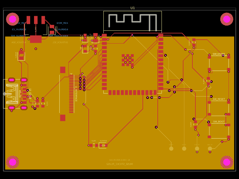 Discover something newShiboSoftwareDev/muse-m5stack-stickc-plus2-replacementA 4-layer ESP32-S3 carrier board with USB-C 5V input, AMS1117 3.3V regulation, buttons, status LED, decoupling passives, and a 24-pin FFC interface for display, touch, audio, or sensor peripherals.