techmannih/nema34-mounted-stepper-controller
A 48 V USB‑C PD 3.1 EPR NEMA‑34 stepper controller PCB combining STM32/TMC5160 control, external MOSFET motor bridges, protected power and regenerative braking, USB data, telemetry, diagnostics, status LEDs, and buzzer alarms.
- Version
- 0.3.92
- License
- unset
- Stars
- 1
docs/indicators.md
# Status, power and alarm circuitry

U35 is PCA9538PWR / C201530 at 7-bit address 0x70. U35, its C95 bypass and the PD_SCL/PD_SDA pullups use PD_3V3. A0/A1 are grounded. The RGB and alarm do not enable the motor.

PC13 / STATUS_GPIO drives U37 SN74LVC1G17DBVR / C7836, a noninverting Schmitt buffer powered by PD_3V3 with C99 100 nF. U37 drives U35_RESET_N; R132 10 kΩ biases its input low and R137 47 kΩ biases its output low. TP_STATUS remains on the MCU side. MCU reset, power loss, USB suspend and failed indicator I2C therefore retain the existing active-low reset behavior.

This buffer is required by the [PCA9538 RESET erratum, §7.2.1.1](https://www.ti.com/lit/ds/symlink/pca9538.pdf): RESET must not be driven high from the independent V3V3_MCU rail while PD_3V3 is absent. The [SN74LVC1G17](https://www.ti.com/lit/ds/symlink/sn74lvc1g17.pdf) has overvoltage-tolerant input and Ioff protection. Its output is sourced from the expander rail. At 3.6 V, R137 loads the high output by 77 µA; including RESET leakage, this stays below the 100 µA VOH test load, giving VCC − 0.1 V minimum. With U37 unpowered, its 10 µA maximum Ioff gives a 0.47 V resistor-only bound; this is bounded leakage, not a zero-current claim. Measure rail ramps, residual RESET voltage and injection on the first article, including slow brownout. Operation below each device's specified supply range is not qualified by this calculation.


D16 is the common-anode NH-B2020RGBA-HF: pin 3 anode, pin 1 red, pin 2 blue and pin 4 green. P0/P1/P2 sink red/green/blue through 1 kΩ/330 Ω/330 Ω. U35 P4–P7 stay inputs tied to GND; INT is intentionally unused. Firmware initializes output latch 0x07 before direction register 0xF0, checks register readback and resets U35 on communication failure. No indicator state enables motion.

| Visible state | Meaning |
|---|---|
| Blue | Commissioning firmware; motion locked |
| Amber | Qualified application waiting for fresh power/temperature telemetry |
| Green | Qualified power/telemetry; query USB STATUS for actual RUN state |
| Red with 200 ms chirp every 2 s | Latched control fault, valid driver fault or measured board temperature at/above 70 °C |
| All off | Reset, absent board supply, USB suspend or indicator I2C failure |

D17 is an independent red power LED through R128 (4.7 kΩ) on **board V3V3**. It does not indicate USB-only MCU power; measure TP_SWD_3V3 for that rail. These additions cannot be powered from USB DATA alone.

BZ1 is an active FUET-9650B-3V buzzer with an internal oscillator. Q26 AO3400A switches its negative lead; R126 (1 kΩ) limits gate charging to below 3.7 mA at a 3.6 V rail, within U35’s 10 mA high-output limit. R127 (100 kΩ) holds the gate low while U35 is reset or unpowered. D18 BAV21W has its cathode on V3V3 and anode on the switched lead. C96 supplies bulk decoupling through a constrained top-layer path of at most 7 mm to the positive terminal. The larger buzzer body needs this longer branch; this is distinct from the IC bypass limits. This alarm is an operator indication, independent of the motor's hardware inhibit chain.

## Design allocations and qualification

Allocate 75 mA additional logic-system current: 60 mA for buzzer margin plus LED, expander, reset buffer and gate/pullup current. Reserve 1.5 mA of the existing 15 mA non-buzzer allocation for the added reset network, including both pulldowns and buffer/RESET supply current. Verify this allocation across independent-rail corners and transitions on the first article. The buzzer specifies at most 30 mA at **3 V** and operates over 2–5 V; the 60 mA allowance at board-rail extremes is a design budget, not a manufacturer maximum or measured result. At 3.6 V the allocation is 0.27 W. The LED/buzzer load is on V3V3; expander and gate-drive current is on PD_3V3. Check combined rail load, supply/OR-device drop and thermal margin at minimum/maximum rail and enclosure temperature.

Nominal RGB currents from typical forward voltages are approximately 1.3 mA red, 1.8 mA green and 1.5 mA blue at 3.3 V before sink-voltage drop. Actual LED brightness and colour balance depend on bins, temperature and rail tolerance; the listed maximum green/blue forward voltage leaves little low-rail headroom. Verify clear visibility at the qualified minimum supply. Power LED current is approximately 0.28 mA at a nominal 2 V forward drop. No optical brightness guarantee is inferred from a schematic.

Firmware host tests cover output polarity, latch-before-direction initialization, alarm duration, reset, missing I2C device, failed initialization writes, expander brownout and USB/power isolation. First-article tests must also verify audible output, cold-boot silence, reset/watchdog silence, rail-current transients and no sound after a bus failure.

Primary sources: [TI PCA9538](https://www.ti.com/lit/ds/symlink/pca9538.pdf), [AOS AO3400A](https://www.aosmd.com/sites/default/files/res/datasheets/AO3400A.pdf), [NationStar LED](https://datasheet.lcsc.com/datasheet/pdf/231c4d2c9a56cafdc8401a79fb0bfc62.pdf?productCode=C2874116), [FUET buzzer](https://datasheet.lcsc.com/datasheet/pdf/108add109d00ccdea1734cb9c944bf18.pdf?productCode=C391032).
Related Packages
 More from this authortechmannih/schematic-testA PCB with a 6-pin SPI display connector linked to SPI signals, ground, and 3.3V power.
 Similar packageimrishabh18/rp2040-motor-controllerAn RP2040-based NEMA17 stepper-motor controller with USB-C programming and PD motor-power negotiation, DRV8825 dual H-bridge drive, current/temperature telemetry, protected power filtering, status RGB LED, buzzer alarm, and optional magnetic encoder.
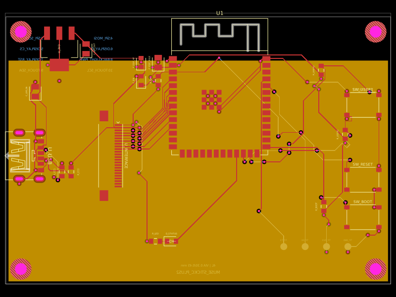 Discover something newShiboSoftwareDev/muse-m5stack-stickc-plus2-replacementA 4-layer ESP32-S3 carrier board with USB-C 5V input, AMS1117 3.3V regulation, buttons, status LED, decoupling passives, and a 24-pin FFC interface for display, touch, audio, or sensor peripherals.