techmannih/nema34-mounted-stepper-controller
A 48 V USB‑C PD 3.1 EPR NEMA‑34 stepper controller PCB combining STM32/TMC5160 control, external MOSFET motor bridges, protected power and regenerative braking, USB data, telemetry, diagnostics, status LEDs, and buzzer alarms.
- Version
- 0.3.92
- License
- unset
- Stars
- 1
docs/assembly.md
# PD1180-EPR — NEMA 34 Smart Motor-Mounted Stepper Controller with USB-C PD 3.1 EPR

## Assembly

The requested deliverable is a fabricated, fully populated, programmed and functionally tested PCBA. Ordering remains on hold. `bun run check:release` checks the documented release gates; it is not a powered test. Follow [the README startup procedure](../README.md#connections-and-operation) and [power-validation.md](power-validation.md) for commissioning.

### Stack and placement

- 85.9 × 85.9 mm, 1.6 mm, four-layer board with four 4.2 mm mounting holes and 1 oz copper on all layers. The fabricator must confirm the USB impedance stack-up; current/thermal qualification remains pending.
- Assembly is top-side only. All fitted components and service pads are on top. U18 alone is on the bottom; its C52/C53 bypass footprints are on top. All three are DNP and omitted from the fitted BOM/CPL and paste. The encoder is centered on the intended motor shaft. Magnet dimensions, air gap, alignment and stray-field effects are validated during mechanical bring-up.
- The ten CSD19534Q5A drain pads contain four connected 0.60/0.30 mm through vias each (40 total), U34 has four exposed-pad thermal vias, and the new U16 ground pad has four. The final top-side route has 63 via drills overlapping top solder lands; exact locations are recorded in `engineering/top-side-placement.json` under `power_eco_via_audit`. Order epoxy-filled and copper-capped processing for every via-in-pad, with no finished via drill below 0.30 mm.
- Check the imported land patterns, solder-mask/paste openings and manufacturer package drawings. JLC/EasyEDA data are a starting point, not a substitute for footprint review.
- Bulk capacitors and JST headers are through-hole; clarify hand/wave/selective assembly with the assembler. Check capacitor polarity and the 25 mm capacitor height.

### Connector pinout

| Connector | Pins in order |
|---|---|
| J1, PD POWER | Dedicated USB-C EPR power; 48 V / 5 A requested contract; no USB data |
| J10, USB DATA | USB 2.0 to STM32 and separate current-limited logic supply; no motor power |
| J2, motor | 1 A1, 2 A2, 3 B1, 4 B2 |
| J3, external brake | 1 VMOTOR, 2 switched resistor return (not a permanent ground) |

Pin numbering follows the imported physical footprints. J7 and the industrial command/transceiver interfaces are removed in the selected onboard-control design. Use the J2/J3 cavity map in [connector-harnesses.md](connector-harnesses.md); housings, contacts, cable and strain relief are separate procurement items. J6/J9 are retired; do not use their historical pinouts.

## Programming and external items

Program U3 with the approved TI-generated TPS26750 full-flash image and U16 with board-specific firmware before motor bring-up. A register-reviewed TI full-flash candidate is included; physical programming/readback is pending. The supplied STM32 image remains for motion-locked commissioning only. Keep POWER_PERMIT and MCU_RUN low in blank/reset/fault states. SWD is a 3.3 V interface provided on labelled top service pads; use a pogo fixture with the adjacent 3.3 V and ground pads.

### Programming and test work order

JLCPCB currently offers [programming](https://jlcpcb.com/help/article/pcba-programming-service) and [functional testing](https://jlcpcb.com/help/article/functional-test-service) for **Standard PCBA**, subject to review of the customer's files, interfaces and test method. Programming takes place after assembly. Request these services explicitly and obtain acceptance for this board's 48 V motor/brake test and fixture; no service has been booked or confirmed here.

Supply the following before approving a ready-to-run batch:

1. Exact board revision and release hashes; matching top BOM/CPL; complete through-hole/tall-part assembly scope; 63 filled/capped via-in-pad locations and the agreed stack-up.
2. U3 **M24512-RMN6TP**: approved full-flash BIN, hash, reviewed EEPROM programming method and readback verification. [TI's EVM guide](https://www.ti.com/lit/ug/slvucp8/slvucp8.pdf) describes generating the full-flash binary. U36 separates U2's EEP_SDA/EEP_SCL I2Cc bus from U3's EEP_PROG_SDA/EEP_PROG_SCL programming pads. Ground TP_PD_ISO before fixed-5 V target power and keep programmer VCC off. Follow [pd-programming.md](pd-programming.md); the constructed fixture still needs qualification. SWD/J10 do not directly program this EEPROM.
3. U16 **STM32G0B1CEU6**: qualified motor-enabled BIN/HEX, hash, SWD pad drawing, flash address `0x08000000` for a raw BIN, supply arrangement and readback procedure. The existing commissioning archive is suitable only for initial diagnostic testing. Do not substitute it as the final motor-operating image.
4. Exact motor and brake load, qualified current/microstep settings, onboard motion limits and stop profile, actual 48 V EPR supply/cable, heatsink, enclosure and ambient limits. These must come from first-article qualification; the 3.8 A RMS design ceiling is not a measured motor rating.
5. An accepted fixture and test procedure: labelled J1 POWER/J10 DATA/J2 motor/J3 brake connections, current limiting, probes, controlled loads, expected readings, stop criteria and an operator demonstration. Agree who performs first-article qualification and who tests the remaining boards.

### Request to send to the assembly/test provider

> Please quote fabrication, complete top-side assembly, programming and pre-shipment functional testing for PD1180-EPR r0.4. Include the through-hole headers/bulk capacitors and the specified filled/capped vias. Please confirm whether your team can commission a 48 V USB-PD EPR controller and qualify its external-MOSFET stepper stage with a supplied motor, brake resistor/heatsink and load fixture. The design target is 5.5 A RMS per phase; that is not yet a qualified operating rating. First-article engineering qualification must precede approval of the motor-enabled firmware and batch acceptance procedure. Each shipped assembly must have verified U3/U16 programming, a controlled STEP/DIR run in both directions and the agreed power/fault tests, with serial-numbered records. Do not ship a blank or motion-locked assembly as ready to run. Please identify the programming interfaces, fixture requirements, first-article test owner, cost and lead time before acceptance. The TI image and final operating envelope are still being prepared; the present package is for engineering review, not production authorization.

This request is prepared but has **not been sent or accepted**. Provider/contact, actual motor/load, maximum speed, stopping profile, supply/cable and brake cooling must be supplied before the work order can be completed.

### First-article programming sequence

1. Approve the exact release manifest and record the board serial. Keep J2 disconnected and hardware enable inactive. The assembly/test provider must approve the fixture's power arrangement; do not connect two independent sources to one supply rail.
2. Program the motion-locked STM32 commissioning image over SWD and verify it, following [firmware/README.md](../firmware/README.md). Capture `HELP`, `STATUS` and `DRIVER` responses; these are diagnostic evidence, not a motor test.
3. Program U3 with the **full-flash** binary generated for this board, verify its complete contents against that binary, then cold-start U2 and record its mode, identity, boot status and negotiated contract. Use the U36-isolated fixture sequence in [pd-programming.md](pd-programming.md). Verify both-wire isolation, target power loss and readback before accepting the fixture; assembled-board access is not yet demonstrated.
4. TI's [SLVAFL1 §2.1–2.2](https://www.ti.com/lit/an/slvafl1/slvafl1.pdf) distinguishes initial full-flash programming from later host updates. The `FLrd`/`FLad`/`FLwd`/`FLvy` update sequence assumes a working application and initialized EEPROM regions. It is not an established blank-board programming path here. Do not load a low-region update file at EEPROM address zero or assume the STM32 commissioning image implements those commands.
5. Complete the no-motor tests in [power-validation.md](power-validation.md), then have the qualification engineer produce and identify a controlled motor-test firmware build. Record every configuration change. Begin below 1 A RMS; increase current only after phase-current, gate and fault measurements pass. The existing commissioning image cannot execute this step.
6. After the agreed motor/load envelope passes, approve the exact motor-enabled image and per-board test revision. Program and verify that image on every shipped board, repeat the acceptance tests, and deliver its hashes and operating settings with the board. A failed test returns to engineering; it never becomes a pass by removing the test or suppressing a protection.

### Acceptance record

No hardware results exist yet. Complete first-article qualification using every applicable row in [power-validation.md](power-validation.md). From that qualified design, approve a repeatable per-board test covering:

| Per-board evidence | Acceptance requirement |
|---|---|
| Assembly inspection | Correct revision/parts, polarity, solder joints, filled/capped lands and all ordered through-hole parts fitted |
| Programming | U3/U16 identity, exact image hashes, successful verify/readback and reset behavior recorded |
| Power and USB | Required rails within qualified limits, negotiated 48 V / 5 A contract, no unintended enable, USB diagnostics and source transitions working |
| Motor operation | Controlled STEP/DIR test in both directions at the approved current/speed/load; record measured phase current and driver status |
| Inhibits and stop | Hardware enable, limits, watchdog/reset and the approved fault tests inhibit motion; no automatic re-arm |
| Thermal/brake | Test at the qualified load/duty/ambient using the approved resistor/heatsink; record bus peak and temperatures against approved limits |
| Handoff | Board serial, inspector/tester, date, instruments, results, firmware/configuration hashes and PASS/FAIL; retain supporting traces/video |

Blank devices, a programmed-but-motion-locked image, a USB-only demo, or an assembly photograph do not meet the requested ready-to-run acceptance. Keep shipment acceptance pending until the agreed tests pass; do not replace missing results with a CAD check. Factory testing against a qualified fixture also does not establish operation with an unspecified motor or load.

The [specified J2 motor harness](motor-harness.md), EPR charger, EPR cable, motor and external braking resistor/heatsink are not assembled PCB components. Their final part numbers and load-dependent ratings are release gates. All populated PCB parts have timestamped JLCSearch evidence; external-brake stock is still unverified.

The exact ordered STEPPERONLINE 34HS31-6004S1 CAD is available in `motor-assembly.circuit.tsx` through `assembly.subassembly`. Direct rear mounting and rotating-shaft access are not established. [Motor assembly](motor-assembly.md) records the proposed front-flange-supported adapter, 10 mm nominal motor-to-PCB gap, screw clearances and unresolved encoder attachment. Approve the shared front interface, tolerances and support strength before fabrication. The former QSH-specific magnet/holder proposal is withdrawn. Do not treat the PD86 mounting-template match as proof of fit to this motor.

## Imported-part corrections

The STM32 component uses explicit ST UFQFPN48 lands, the GP pin map, a grounded exposed pad and a courtyard. CSD19534 drain thermal vias are implemented in the final KiCad route with explicit drain-net identities and bottom copper ties. Q2/Q3 use the exact CSD17484F4 PicoStar-3 land pattern and G/S/D pin map from the imported JLC part. BAV21 polarity is explicit, bulk capacitor pads carry polarity aliases, imported transistor symbols have reference text, and vertical headers specify top-side cable insertion.

## PD power-path enable buffer

Fit Q2/Q3 as CSD17484F4 (`C2862245`), R9/R12 as 0 Ω (`C21189`), and R11/R13 as 100 kΩ (`C25803`). Both pull-ups terminate at `PD_3V3`, U2's LDO_3V3 rail. This is the two-NMOS non-inverting buffer in the TPS26750 EVM and Figure 8-5 of the TPS26750 datasheet. R10 is intentionally absent; do not add the retired BJT base pull-down.

## Logic backup supply

U22, L2 and U24 provide motor-side logic backup; U5, L1 and U23 provide PD-side startup. Fit both LM66100 parts and R111. The wiring follows TI Figure 17: U23 CE senses V3V3_MOTOR, U23 ST and U24 CE share LOGIC_OR_PRIORITY, and R111 pulls that interlock up to V3V3_PD. U24 ST is grounded because it is unused. U26/U27 separately combine board V3V3 and DATA-derived V3V3_USB into V3V3_MCU. Do not substitute the simpler common-output CE wiring; equal inputs can turn both devices off. The 3.3 V service pads are logic references; an external accessory current budget has not been allocated.

## Indicator and programming-fixture acceptance

Verify the new top-side D16/D17/BZ1/Q26/U35/U36 parts and their polarity against the source/BOM, with R126 = 1 kΩ and R127 = 100 kΩ. Check the 19 bare service contacts against the fixture map in [pd-programming.md](pd-programming.md). The indicators consume board V3V3 and do not imply motor permission or correct PD programming. Verify RGB visibility, power indication, fault chirps, silent reset and the combined rail current using [indicators.md](indicators.md). Record these tests with the per-board firmware/configuration hashes.

Complete the serial-numbered programming/readback and cold-boot checklist in [readiness.md](readiness.md), then the supply/fault → low-current motion → brake/thermal sequence. Follow [manufacturing-acceptance.md](manufacturing-acceptance.md) for ENIG, all 63 filled/capped via-in-pad locations, stack-up, shorter USB stakes, actual mounting and harness acceptance. **10 Ω/300 W remains provisional; motion locks remain enabled.**
Related Packages
 More from this authortechmannih/schematic-testA PCB with a 6-pin SPI display connector linked to SPI signals, ground, and 3.3V power.
 Similar packageimrishabh18/rp2040-motor-controllerAn RP2040-based NEMA17 stepper-motor controller with USB-C programming and PD motor-power negotiation, DRV8825 dual H-bridge drive, current/temperature telemetry, protected power filtering, status RGB LED, buzzer alarm, and optional magnetic encoder.
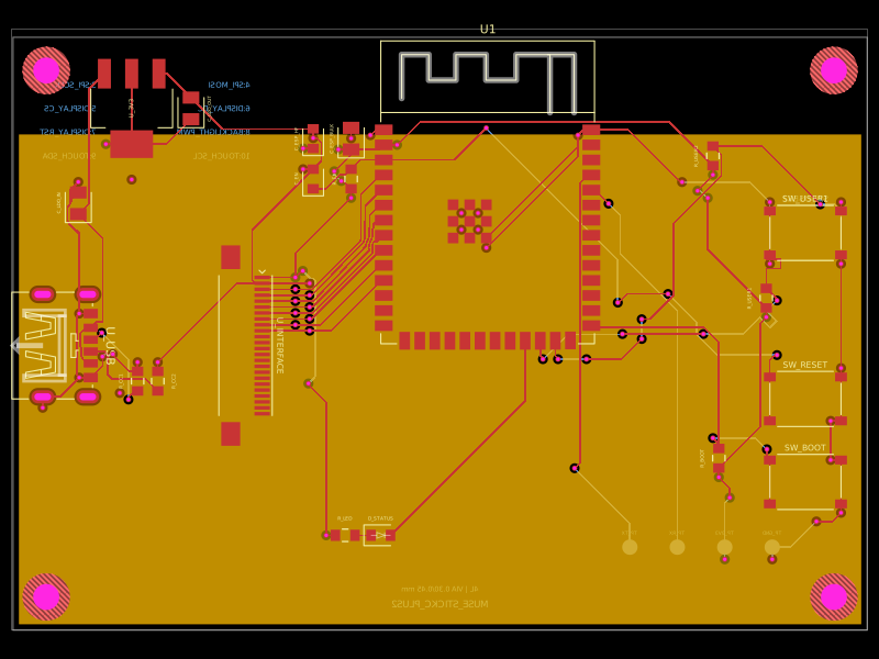 Discover something newShiboSoftwareDev/muse-m5stack-stickc-plus2-replacementA 4-layer ESP32-S3 carrier board with USB-C 5V input, AMS1117 3.3V regulation, buttons, status LED, decoupling passives, and a 24-pin FFC interface for display, touch, audio, or sensor peripherals.