techmannih/museview
A 50×35 mm USB‑C 5 V camera board combining an ESP32‑S3 module, M0031 parallel camera connector, buck/LDO power rails, USB/ESD protection, controls, status LED, and passives.
- Version
- 0.1.18
- License
- unset
- Stars
- 1
index.circuit.tsx
PCB
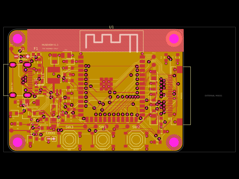
Schematic

import "tscircuit"
import { Fragment } from "react"
import { ESP32_S3_WROOM_1_N16R8 } from "./imports/ESP32_S3_WROOM_1_N16R8/ESP32_S3_WROOM_1_N16R8"
import { TYPE_C_31_M_12 } from "./imports/TYPE_C_31_M_12/TYPE_C_31_M_12"
import { AFC01_S24FCA_00 } from "./imports/AFC01_S24FCA_00/AFC01_S24FCA_00"
import { USBLC6_2SC6 } from "./imports/USBLC6_2SC6/USBLC6_2SC6"
import { BSMD0603_075_6V } from "./imports/BSMD0603_075_6V/BSMD0603_075_6V"
import { SMF5_0A } from "./imports/SMF5_0A/SMF5_0A"
import { TLV62569DBVR } from "./imports/TLV62569DBVR/TLV62569DBVR"
import { WPN4020H2R2MT } from "./imports/WPN4020H2R2MT/WPN4020H2R2MT"
import { XC6206P282MR } from "./imports/XC6206P282MR/XC6206P282MR"
import { SGM2059_ADJXN5G_TR } from "./imports/SGM2059_ADJXN5G_TR/SGM2059_ADJXN5G_TR"
import { TS_1187A_B_A_B } from "./imports/TS_1187A_B_A_B/TS_1187A_B_A_B"
import { KT_0603R } from "./imports/KT_0603R/KT_0603R"
import { C, R } from "./imports/passives"
import { boardRouter } from "./scripts/board-router"

/** MuseView V1. Standard USB-C 5 V sink, no USB-PD controller.
 * Electrical values and pin assignments follow the component datasheets.
 * VDD_IO is intentionally 3.192 V nominal: a common ESP32/camera I/O domain.
 */
export const MuseViewV1 = () => (
  <board name="MUSEVIEW_V1" title="MuseView V1 · USB-C 5 V camera"
    width="50mm" height="35mm" borderRadius="2.5mm" layers={4} thickness="1.6mm"
    solderMaskColor="#181e22" minTraceWidth="0.15mm" defaultTraceWidth="0.2mm"
    minViaHoleDiameter={0.3} minViaPadDiameter={0.45} minViaEdgeToPadEdgeClearance="0.15mm" minBoardEdgeClearance="0.25mm" minTraceToHoleEdgeClearance="0.23mm"
    pcbStyle={{ viaPadDiameter: 0.6, viaHoleDiameter: 0.3 }}
    autorouterVersion="beta_pipeline9" autorouter={{algorithmFn:boardRouter,local:true,allowViaInPad:false,traceClearance:0.18}} autorouterEffortLevel="5x"
    schAutoLayoutEnabled schTraceAutoLabelEnabled schMaxTraceDistance="1.2mm">

    <schematicsheet name="usb" displayName="USB-C input and protection" sheetIndex={1} sheetSize="ANSI_B" sheetWidth="360mm" sheetHeight="280mm">
      <schematictext schX={0} schY={12} fontSize={0.5} text={"01 \u00b7 USB-C INPUT / PROTECTION"} />
      <schematictext schX={0} schY={-10} fontSize={0.28} anchor="center" text={"5 V ONLY · Independent 5.1k CC pull-downs"} />
      <schematictext schX={0} schY={-10.45} fontSize={0.28} anchor="center" text={"Native USB: GPIO19 D− / GPIO20 D+"} />
      <schematictext schX={0} schY={-10.9} fontSize={0.28} anchor="center" text={"33R source termination. No Power Delivery negotiation."} />
    </schematicsheet>
    <schematicsheet name="power" displayName="Main and camera power" sheetIndex={2} sheetSize="ANSI_B" sheetWidth="360mm" sheetHeight="280mm">
      <schematictext schX={0} schY={12} fontSize={0.5} text={"02 \u00b7 POWER SUPPLIES"} />
      <schematictext schX={0} schY={10} fontSize={0.28} anchor="center" text={"U3: 0.6 × (1 + 432k / 100k) = 3.192 V"} />
      <schematictext schX={0} schY={9.55} fontSize={0.28} anchor="center" text={"R6/R7 must be 0.1%. Shared MCU/camera I/O supply."} />
      <schematictext schX={0} schY={9.1} fontSize={0.28} anchor="center" text={"U5: 0.793 × (1 + 25.5k / 40.2k) = 1.296 V"} />
    </schematicsheet>
    <schematicsheet name="mcu" displayName="ESP32, controls and recovery" sheetIndex={3} sheetSize="ANSI_B" sheetWidth="360mm" sheetHeight="280mm">
      <schematictext schX={0} schY={12} fontSize={0.5} text={"03 \u00b7 ESP32 / CONTROLS"} />
      <schematictext schX={0} schY={-11} fontSize={0.28} anchor="center" text={"N16R8: internal flash, PSRAM and 2.4 GHz Wi-Fi"} />
      <schematictext schX={0} schY={-11.45} fontSize={0.28} anchor="center" text={"GPIO35/36/37 reserved for octal PSRAM: unconnected"} />
      <schematictext schX={0} schY={-11.9} fontSize={0.28} anchor="center" text={"Hold BOOT, tap RESET, release BOOT for ROM recovery."} />
    </schematicsheet>
    <schematicsheet name="camera" displayName="M0031 DVP camera interface" sheetIndex={4} sheetSize="ANSI_B" sheetWidth="360mm" sheetHeight="280mm">
      <schematictext schX={0} schY={12} fontSize={0.5} text={"04 \u00b7 M0031 CAMERA INTERFACE"} />
      <schematictext schX={0} schY={10} fontSize={0.28} anchor="center" text={"External Arducam M0031 · 24 contacts · 0.5 mm pitch"} />
      <schematictext schX={0} schY={9.55} fontSize={0.28} anchor="center" text={"Camera is fitted by hand after PCBA. Contacts toward PCB."} />
      <schematictext schX={0} schY={9.1} fontSize={0.28} anchor="center" text={"Driver D0–D7 = sensor D2–D9. STROBE/D0/D1 unused."} />
    </schematicsheet>

    <schematicsection name="usb-port" displayName="USB-C device and shield" />
    <schematicsection name="usb-data" displayName="ESD and data termination" />
    <schematicsection name="buck" displayName="5 V to 3.192 V" />
    <schematicsection name="camera-regulators" displayName="2.8 V analog / 1.296 V core" />
    <schematicsection name="processor" displayName="ESP32-S3-WROOM-1-N16R8" />
    <schematicsection name="controls" displayName="BOOT / RESET / ASK / status" />
    <schematicsection name="camera-interface" displayName="24-pin camera contract" />

    {/* Route power distribution before signal buses. */}
    <net name="GND" isGroundNet />
    <net name="USB_RAW_5V" isPowerNet />
    <net name="VBUS_5V" isPowerNet />
    <net name="VDD_IO" isPowerNet />
    <net name="CAM_2V8" isPowerNet />
    <net name="CAM_1V3" isPowerNet />
    <net name="BUCK_SW" isPowerNet={false} />
    <net name="BUCK_FB" isPowerNet={false} />
    <net name="CAM_FB" isPowerNet={false} />
    <net name="USB_SHIELD" isPowerNet={false} />

    {/* L2 reference remains unbroken. Signal routing uses outer layers. */}
    <copperpour name="GND_PLANE" layer="inner1" connectsTo="net.GND" unbroken clearance="0.2mm" boardEdgeMargin="0.3mm" />
    <copperpour name="VDD_PLANE" layer="inner2" connectsTo="net.VDD_IO" unbroken clearance="0.2mm" boardEdgeMargin="0.3mm" />
    <keepout shape="rect" layers={["top", "inner1", "inner2", "bottom"]}
      excludeRefs={[".U1"]} pcbX={2.75} pcbY={14.275} width="44.5mm" height="6.45mm" />
    {([[-22.25, 14.75], [22.25, 14.75], [-22.25, -14.75], [22.25, -14.75]] as const).map(([x,y],i) => (
      <Fragment key={`mount-${i}`}>
        <hole name={`H${i+1}`} pcbX={x} pcbY={y} diameter="2.7mm" />
        <keepout shape="circle" radius="2.3mm" pcbX={x} pcbY={y} layers={["top", "inner1", "inner2", "bottom"]} />
      </Fragment>
    ))}

    <TYPE_C_31_M_12 name="J1" displayName="J1 · USB-C 5 V" layer="top" noConnect={["SBU1", "SBU2"]}
      pcbX={-20.85} pcbY={3} pcbRotation={-90}
      schX={-10} schY={2} schWidth={1.2} schHeight={3.6} schSheetName="usb" schSectionName="usb-port"
      connections={{ EH1:"net.USB_SHIELD", EH2:"net.USB_SHIELD", EH3:"net.USB_SHIELD", EH4:"net.USB_SHIELD",
        CC1:"net.CC1", CC2:"net.CC2", DN1:"net.USB_DM_PORT", DN2:"net.USB_DM_PORT", DP1:"net.USB_DP_PORT", DP2:"net.USB_DP_PORT",
        GND1:"net.GND", GND2:"net.GND", VBUS1:"net.USB_RAW_5V", VBUS2:"net.USB_RAW_5V" }} />
    <R name="R1" part="r5k1" pcbX={-16} pcbY={8} pcbRotation={90}
      schX={-10} schY={-3.5} schOrientation="vertical" schSheetName="usb" schSectionName="usb-port"
      connections={{pin1:"net.CC1",pin2:"net.GND"}} />
    <R name="R2" part="r5k1" pcbX={-16} pcbY={5} pcbRotation={90}
      schX={-6.5} schY={-3.5} schOrientation="vertical" schSheetName="usb" schSectionName="usb-port"
      connections={{pin1:"net.CC2",pin2:"net.GND"}} />
    <R name="R5" part="r1m" pcbX={-22.1} pcbY={-3.3} pcbRotation={0}
      schX={-10} schY={-7} schOrientation="vertical" schSheetName="usb" schSectionName="usb-port"
      connections={{pin1:"net.USB_SHIELD",pin2:"net.GND"}} />
    <C name="C1" part="c4n7" pcbX={-18} pcbY={-3.45} pcbRotation={0}
      schX={-6.5} schY={-7} schOrientation="vertical" schSheetName="usb" schSectionName="usb-port"
      connections={{pin1:"net.USB_SHIELD",pin2:"net.GND"}} />
    <USBLC6_2SC6 name="U2" layer="top" pcbX={-15.7} pcbY={0} pcbRotation={-90}
      schX={-2} schY={2} schWidth={1.8} schHeight={0.8} schSheetName="usb" schSectionName="usb-data"
      connections={{pin1:"net.USB_DM_PORT",pin2:"net.GND",pin3:"net.USB_DP_PORT",pin4:"net.USB_DP_ESD",pin5:"net.VBUS_5V",pin6:"net.USB_DM_ESD"}} />
    <C name="C18" part="c100n" pcbX={-16.1} pcbY={2.6} pcbRotation={180}
      schX={3} schY={7} schOrientation="vertical" schSheetName="usb" schSectionName="usb-data"
      connections={{pin1:"net.VBUS_5V",pin2:"net.GND"}} />
    <R name="R3" part="r33" pcbX={-7} pcbY={-5.395} pcbRotation={0}
      schX={4} schY={3} schSheetName="usb" schSectionName="usb-data"
      connections={{pin1:"net.USB_DM_ESD",pin2:"net.USB_DM_MCU"}} />
    <R name="R4" part="r33" pcbX={-7} pcbY={-7.295} pcbRotation={0}
      schX={4} schY={0} schSheetName="usb" schSectionName="usb-data"
      connections={{pin1:"net.USB_DP_ESD",pin2:"net.USB_DP_MCU"}} />
    <BSMD0603_075_6V name="F1" displayName="F1 · 750 mA PTC" pcbX={-17} pcbY={10.3} pcbRotation={0}
      schX={-10} schY={7.5} schRotation={-90} schSheetName="usb" schSectionName="usb-port"
      connections={{pin1:"net.USB_RAW_5V",pin2:"net.VBUS_5V"}} />
    <SMF5_0A name="D1" displayName="D1 · SMF5.0A" pcbX={-21} pcbY={9.7} pcbRotation={0}
      schX={-3} schY={7.5} schRotation={0} schSheetName="usb" schSectionName="usb-port"
      connections={{cathode:"net.VBUS_5V",anode:"net.GND"}} />

    <TLV62569DBVR name="U3" pcbX={-11} pcbY={-1.5} layer="top" pcbRotation={90}
      schX={-7} schY={5} schWidth={1.65} schHeight={0.6} schSheetName="power" schSectionName="buck"
      schPinArrangement={{leftSide:{pins:["VIN","EN"],direction:"top-to-bottom"},rightSide:{pins:["SW","FB"],direction:"top-to-bottom"},bottomSide:{pins:["GND"],direction:"left-to-right"}}} connections={{VIN:"net.VBUS_5V",EN:"net.VBUS_5V",GND:"net.GND",SW:"net.BUCK_SW",FB:"net.BUCK_FB"}} />
    <WPN4020H2R2MT name="L1" pcbX={-11.95} pcbY={4.35} pcbRotation={90}
      schX={-2} schY={6} schSheetName="power" schSectionName="buck"
      connections={{pin1:"net.BUCK_SW",pin2:"net.VDD_IO"}} />
    <C name="C2" part="c4u7" pcbX={-11.95} pcbY={-9.3} pcbRotation={270}
      schX={-13.2} schY={0} schOrientation="vertical" schSheetName="power" schSectionName="buck"
      connections={{pin1:"net.VBUS_5V",pin2:"net.GND"}} />
    <C name="C3" part="c100n" pcbX={-11.95} pcbY={-5.3} pcbRotation={270}
      schX={-12} schY={0} schOrientation="vertical" schSheetName="power" schSectionName="buck"
      connections={{pin1:"net.VBUS_5V",pin2:"net.GND"}} />
    <C name="C4" part="c10u" pcbX={-11.7} pcbY={9.1} pcbRotation={90}
      schX={2.8} schY={-2} schOrientation="vertical" schSheetName="power" schSectionName="buck"
      connections={{pin1:"net.VDD_IO",pin2:"net.GND"}} />
    <R name="R6" part="r432k" pcbX={-7.8} pcbY={-3} pcbRotation={90}
      schX={0} schY={2.5} schOrientation="vertical" schSheetName="power" schSectionName="buck"
      connections={{pin1:"net.VDD_IO",pin2:"net.BUCK_FB"}} />
    <R name="R7" part="r100k" pcbX={-7.8} pcbY={0.05} pcbRotation={270}
      schX={0} schY={-4.5} schOrientation="vertical" schSheetName="power" schSectionName="buck"
      connections={{pin1:"net.BUCK_FB",pin2:"net.GND"}} />
    <C name="C5" part="c6p8" pcbX={-9.4} pcbY={-7.8} pcbRotation={270}
      schX={1.6} schY={-2} schOrientation="vertical" schSheetName="power" schSectionName="buck"
      connections={{pin1:"net.VDD_IO",pin2:"net.BUCK_FB"}} />

    <XC6206P282MR name="U4" pcbX={-20} pcbY={-6.5} layer="top" pcbRotation={0}
      schX={-8} schY={-6} schWidth={1.8} schHeight={1.5} schSheetName="power" schSectionName="camera-regulators"
      schPinArrangement={{leftSide:{pins:["VIN"],direction:"top-to-bottom"},rightSide:{pins:["VOUT"],direction:"top-to-bottom"},bottomSide:{pins:["VSS"],direction:"left-to-right"}}} connections={{VSS:"net.GND",VIN:"net.VBUS_5V",VOUT:"net.CAM_2V8"}} />
    <C name="C6" part="c1u" pcbX={-23.4} pcbY={-6.5} pcbRotation={180}
      schX={-10.8} schY={0} schOrientation="vertical" schSheetName="power" schSectionName="camera-regulators"
      connections={{pin1:"net.VBUS_5V",pin2:"net.GND"}} />
    <C name="C7" part="c1u" pcbX={-16.6} pcbY={-6.5} pcbRotation={0}
      schX={-3} schY={-6} schOrientation="vertical" schSheetName="power" schSectionName="camera-regulators"
      connections={{pin1:"net.CAM_2V8",pin2:"net.GND"}} />
    <SGM2059_ADJXN5G_TR name="U5" pcbX={-18} pcbY={-10.7} layer="top" pcbRotation={0}
      schX={7} schY={-3} schWidth={1.65} schHeight={0.6} schSheetName="power" schSectionName="camera-regulators"
      schPinArrangement={{leftSide:{pins:["IN","EN"],direction:"top-to-bottom"},rightSide:{pins:["OUT","FB"],direction:"top-to-bottom"},bottomSide:{pins:["GND"],direction:"left-to-right"}}} connections={{IN:"net.VDD_IO",EN:"net.VDD_IO",GND:"net.GND",OUT:"net.CAM_1V3",FB:"net.CAM_FB"}} />
    <C name="C8" part="c1u" pcbX={-14.4} pcbY={-10.7} pcbRotation={0}
      schX={4} schY={-2} schOrientation="vertical" schSheetName="power" schSectionName="camera-regulators"
      connections={{pin1:"net.VDD_IO",pin2:"net.GND"}} />
    <C name="C9" part="c1u" pcbX={-18.6} pcbY={-14.2} pcbRotation={270}
      schX={12} schY={-3} schOrientation="vertical" schSheetName="power" schSectionName="camera-regulators"
      connections={{pin1:"net.CAM_1V3",pin2:"net.GND"}} />
    <R name="R8" part="r25k5" pcbX={-14.8} pcbY={-8.2} pcbRotation={0}
      schX={7} schY={-7} schSheetName="power" schSectionName="camera-regulators"
      schOrientation="vertical" connections={{pin1:"net.CAM_1V3",pin2:"net.CAM_FB"}} />
    <R name="R9" part="r40k2" pcbX={-22.2} pcbY={-9.5} pcbRotation={180}
      schX={12} schY={-7} schSheetName="power" schSectionName="camera-regulators"
      schOrientation="vertical" connections={{pin1:"net.CAM_FB",pin2:"net.GND"}} />

    <ESP32_S3_WROOM_1_N16R8 name="U1" layer="top" pcbX={4.5} pcbY={0.5} pcbRotation={0}
      schX={-3} schY={0} schWidth={1.96} schHeight={4.4} schSheetName="mcu" schSectionName="processor"
      connections={{GND1:"net.GND",GND2:"net.GND",GND3:"net.GND","3V3":"net.VDD_IO",EN:"net.ESP_EN",IO0:"net.BOOT",
        IO4:"net.CAM_SDA",IO5:"net.CAM_SCL",IO6:"net.CAM_VSYNC",IO7:"net.CAM_HREF",IO15:"net.CAM_XCLK",
        IO9:"net.CAM_D2",IO10:"net.CAM_D3",IO11:"net.CAM_D4",IO12:"net.CAM_D5",IO13:"net.CAM_D6",IO14:"net.CAM_D7",IO21:"net.CAM_D8",IO47:"net.CAM_D9",IO48:"net.CAM_PCLK",
        IO16:"net.ASK",IO17:"net.LED_DRIVE",IO18:"net.CAM_RESET",IO8:"net.CAM_PWDN",IO19:"net.USB_DM_MCU",IO20:"net.USB_DP_MCU",
        RXD0:"net.UART_RX",TXD0:"net.UART_TX",IO39:"net.JTAG_TCK",IO40:"net.JTAG_TDO",IO41:"net.JTAG_TDI",IO42:"net.JTAG_TMS"}} />
    <C name="C10" part="c100n" pcbX={-7.5} pcbY={8.275} pcbRotation={180}
      schX={-11.2} schY={2} schOrientation="vertical" schSheetName="mcu" schSectionName="processor"
      connections={{pin1:"net.VDD_IO",pin2:"net.GND"}} />
    <C name="C11" part="c10u" pcbX={-8.5} pcbY={10} pcbRotation={180}
      schX={-10} schY={2} schOrientation="vertical" schSheetName="mcu" schSectionName="processor"
      connections={{pin1:"net.VDD_IO",pin2:"net.GND"}} />
    <R name="R10" part="r10k" pcbX={-7.5} pcbY={6.4} pcbRotation={0}
      schX={5} schY={2} schSheetName="mcu" schSectionName="controls"
      schOrientation="vertical" connections={{pin1:"net.VDD_IO",pin2:"net.ESP_EN"}} />
    <C name="C12" part="c1u" pcbX={-8} pcbY={4.5} pcbRotation={0}
      schX={11} schY={6} schOrientation="vertical" schSheetName="mcu" schSectionName="controls"
      connections={{pin1:"net.ESP_EN",pin2:"net.GND"}} />
    <R name="R11" part="r10k" pcbX={18.6} pcbY={-8.7} pcbRotation={90}
      schX={7} schY={2} schSheetName="mcu" schSectionName="controls"
      schOrientation="vertical" connections={{pin1:"net.VDD_IO",pin2:"net.BOOT"}} />
    <R name="R12" part="r10k" pcbX={-7.5} pcbY={2.8} pcbRotation={0}
      schX={7} schY={-3.5} schSheetName="mcu" schSectionName="controls"
      schOrientation="vertical" connections={{pin1:"net.VDD_IO",pin2:"net.ASK"}} />
    <TS_1187A_B_A_B name="SW1" displayName="SW1 · RESET" pcbX={2} pcbY={-14} pcbRotation={0}
      schX={7} schY={5.2} schSheetName="mcu" schSectionName="controls"
      connections={{A:"net.ESP_EN",C:"net.ESP_EN",B:"net.GND",D:"net.GND"}} />
    <TS_1187A_B_A_B name="SW2" displayName="SW2 · BOOT" pcbX={11.5} pcbY={-14} pcbRotation={0}
      schX={7} schY={-0.2} schSheetName="mcu" schSectionName="controls"
      connections={{A:"net.BOOT",C:"net.BOOT",B:"net.GND",D:"net.GND"}} />
    <TS_1187A_B_A_B name="SW3" displayName="SW3 · ASK" pcbX={-7.5} pcbY={-14} pcbRotation={0}
      schX={7} schY={-5.8} schSheetName="mcu" schSectionName="controls"
      connections={{A:"net.ASK",C:"net.ASK",B:"net.GND",D:"net.GND"}} />
    <R name="R13" part="r1k" pcbX={-16} pcbY={-13.8} pcbRotation={0}
      schX={7} schY={-9} schSheetName="mcu" schSectionName="controls"
      connections={{pin1:"net.LED_DRIVE",pin2:"net.LED_A"}} />
    <KT_0603R name="LED1" pcbX={-12.7} pcbY={-13.8} pcbRotation={0}
      schX={11} schY={-9} schSheetName="mcu" schSectionName="controls"
      schOrientation="vertical" connections={{anode:"net.LED_A",cathode:"net.GND"}} />

    {/* All nine segmented EPAD lands remain exposed for solder paste. The
        solder-mask-covered island and through-vias connect them to L2 GND. */}
    <copperpour name="EPAD_GND" layer="top" connectsTo="net.GND" coveredWithSolderMask useThermalReliefs={false}
      outline={[{x:1.15,y:-.05},{x:4.85,y:-.05},{x:4.85,y:3.75},{x:1.15,y:3.75}]} clearance="0.15mm" />
    {([2.299852,3.6999] as const).flatMap(x => [1.12485,2.5249].map(y =>
      <Fragment key={`epad-${x}-${y}`}><via name={`EPAD_${x}_${y}`} pcbX={x} pcbY={y} connectsTo="net.GND"
        fromLayer="top" toLayer="bottom" holeDiameter="0.3mm" outerDiameter="0.6mm" /></Fragment>
    ))}

    <AFC01_S24FCA_00 name="J2" displayName="J2 · M0031" pcbX={22.6} pcbY={-1.5} layer="top" noConnect={["pin1", "pin23", "pin24"]} pcbRotation={90}
      schX={5} schY={0} schWidth={2.5} schHeight={2.8} schSheetName="camera" schSectionName="camera-interface"
      connections={{pin2:"net.GND",pin3:"net.CAM_SDA",pin4:"net.CAM_2V8",pin5:"net.CAM_SCL",pin6:"net.CAM_RESET",pin7:"net.CAM_VSYNC",pin8:"net.CAM_PWDN",pin9:"net.CAM_HREF",pin10:"net.CAM_1V3",pin11:"net.VDD_IO",pin12:"net.CAM_D9",pin13:"net.CAM_XCLK",pin14:"net.CAM_D8",pin15:"net.GND",pin16:"net.CAM_D7",pin17:"net.CAM_PCLK",pin18:"net.CAM_D6",pin19:"net.CAM_D2",pin20:"net.CAM_D5",pin21:"net.CAM_D3",pin22:"net.CAM_D4",pin25:"net.GND",pin26:"net.GND"}} />
    <R name="R14" part="r4k7" pcbX={20} pcbY={9.4} pcbRotation={90}
      schX={-10} schY={-6} schOrientation="vertical" schSheetName="camera" schSectionName="camera-interface"
      connections={{pin1:"net.VDD_IO",pin2:"net.CAM_SDA"}} />
    <R name="R15" part="r4k7" pcbX={23.3} pcbY={9.4} pcbRotation={90}
      schX={-6} schY={-6} schOrientation="vertical" schSheetName="camera" schSectionName="camera-interface"
      connections={{pin1:"net.VDD_IO",pin2:"net.CAM_SCL"}} />
    <R name="R16" part="r10k" pcbX={18.7} pcbY={-11.7} pcbRotation={0}
      schX={-10} schY={-10} schOrientation="vertical" schSheetName="camera" schSectionName="camera-interface"
      connections={{pin1:"net.CAM_RESET",pin2:"net.GND"}} />
    <R name="R17" part="r10k" pcbX={17.5} pcbY={-14.7} pcbRotation={0}
      schX={-6} schY={-10} schOrientation="vertical" schSheetName="camera" schSectionName="camera-interface"
      connections={{pin1:"net.VDD_IO",pin2:"net.CAM_PWDN"}} />
    <C name="C13" part="c100n" pcbX={16.5} pcbY={-4.924928} pcbRotation={90}
      schX={-7.2} schY={5} schOrientation="vertical" schSheetName="camera" schSectionName="camera-interface"
      connections={{pin1:"net.CAM_2V8",pin2:"net.GND"}} />
    <C name="C14" part="c100n" pcbX={16.5} pcbY={-1.924934} pcbRotation={90}
      schX={-7.2} schY={1} schOrientation="vertical" schSheetName="camera" schSectionName="camera-interface"
      connections={{pin1:"net.CAM_1V3",pin2:"net.GND"}} />
    <C name="C15" part="c100n" pcbX={16.5} pcbY={1.2} pcbRotation={90}
      schX={-10} schY={-2.5} schOrientation="vertical" schSheetName="camera" schSectionName="camera-interface"
      connections={{pin1:"net.VDD_IO",pin2:"net.GND"}} />
    <C name="C16" part="c4u7" pcbX={16.5} pcbY={-8.15} pcbRotation={90}
      schX={-6} schY={5} schOrientation="vertical" schSheetName="camera" schSectionName="camera-interface"
      connections={{pin1:"net.CAM_2V8",pin2:"net.GND"}} />
    <C name="C17" part="c4u7" pcbX={16.5} pcbY={4.4} pcbRotation={90}
      schX={-6} schY={1} schOrientation="vertical" schSheetName="camera" schSectionName="camera-interface"
      connections={{pin1:"net.CAM_1V3",pin2:"net.GND"}} />

    {/* Probe pads are PCB features, not JLC assembly components. */}
    {([
      ["TP1","UART_TX",-3,-10.25, -11,-3,"mcu"], ["TP2","UART_RX",0,-10.25, -11,-5,"mcu"],
      ["TP3","VDD_IO",3,-10.25, -11,-7,"mcu"], ["TP4","GND",6,-10.25, -11,-9,"mcu"],
      ["TP5","VBUS_5V",-24,11.9, 9,7,"usb"], ["TP6","CAM_2V8",-20.8,12, 12,-7,"camera"],
      ["TP7","CAM_1V3",-24,-11.4, 12,-10,"camera"],
      ["TP8","JTAG_TCK",9,-10.25, 13,4,"mcu"], ["TP9","JTAG_TDO",12,-10.25, 13,2,"mcu"],
      ["TP10","JTAG_TDI",16.5,7.3, 13,0,"mcu"], ["TP11","JTAG_TMS",16.5,9.6, 13,-2,"mcu"],
    ] as const).map(([name,net,x,y,sx,sy,sheet]) => <testpoint key={name} name={name} doNotPlace
      footprintVariant="pad" padShape="circle" padDiameter="1.2mm" layer="top" pcbX={x} pcbY={y}
      schX={sx} schY={sy} schSheetName={sheet} connections={{pin1:`net.${net}`}}>
      <courtyardoutline outline={[{x:-.65,y:-.65},{x:.65,y:-.65},{x:.65,y:.65},{x:-.65,y:.65},{x:-.65,y:-.65}]} />
    </testpoint>)}

    <trace name="USB_DM_TO_R" from=".U2 > .pin6" to=".R3 > .pin1" thickness="0.2mm" />
    <trace name="USB_DP_TO_R" from=".U2 > .pin4" to=".R4 > .pin1" thickness="0.2mm" />
    <trace name="USB_DM_TO_MCU" from=".R3 > .pin2" to=".U1 > .IO19" pcbStraightLine thickness="0.2mm" />
    <trace name="USB_DP_TO_MCU" from=".R4 > .pin2" to=".U1 > .IO20" pcbStraightLine thickness="0.2mm" />

    {/* Fixed high-frequency bypass paths and their local L2 returns. */}
    <trace name="DECOUPLE_C13" from=".J2 > .pin4" to=".C13 > .pin1" pcbStraightLine thickness="0.15mm" maxLength="5.1mm" />
    <trace name="DECOUPLE_C14" from=".J2 > .pin10" to=".C14 > .pin1" pcbStraightLine thickness="0.15mm" maxLength="5.1mm" />
    <trace name="DECOUPLE_C3" from=".U3 > .VIN" to=".C3 > .pin1" pcbStraightLine thickness="0.25mm" maxLength="3mm" />
    <trace name="DECOUPLE_C10" from=".U1 > .3V3" to=".C10 > .pin1" pcbStraightLine thickness="0.4mm" maxLength="3mm" />
    <trace name="DECOUPLE_C6" from=".U4 > .VIN" to=".C6 > .pin1" pcbStraightLine thickness="0.3mm" maxLength="3mm" />
    <trace name="DECOUPLE_C8" from=".U5 > .IN" to=".C8 > .pin1" pcbStraightLine thickness="0.3mm" maxLength="3mm" />
    {/* pcbPath coordinates are local to U2, which is rotated -90 degrees. */}
    <trace name="DECOUPLE_C18" from=".U2 > .pin5" to=".C18 > .pin1" pcbPath={[{x:0,y:0.05},{x:-1.7,y:0.05}]} thickness="0.25mm" maxLength="4mm" />
    <trace name="BUCK_SWITCH" from=".U3 > .SW" to=".L1 > .pin1" pcbStraightLine thickness="0.6mm" maxLength="3mm" />
    <trace name="BUCK_OUTPUT" from=".L1 > .pin2" to=".C4 > .pin1" pcbStraightLine thickness="0.4mm" maxLength="3mm" />
    {([
      ["C2",-11.95,-11.1],
      ["C3",-11.95,-6.9],
      ["C4",-13,10.1],
      ["C6",-24.3,-7.4],
      ["C7",-15,-6.5],
      ["C8",-12.8,-10.7],
      ["C9",-18.6,-15.85],
      ["C10",-9.1,8.275],
      ["C11",-10.4,10],
      ["C12",-6.4,4.5],
      ["C13",15.7,-4.099928],
      ["C14",15.7,-1.099934],
      ["C15",15.7,2.025],
      ["C16",15.6,-7.125],
      ["C17",15.6,5.425],
      ["C18",-16.925,1.9],
    ] as const).map(([cap,x,y]) => <Fragment key={`return-${cap}`}>
      <via name={`GND_${cap}`} pcbX={x} pcbY={y} fromLayer="top" toLayer="bottom" connectsTo="net.GND" outerDiameter="0.6mm" holeDiameter="0.3mm" />
      <trace name={`RETURN_${cap}`} from={`.${cap} > .pin2`} to={`.GND_${cap} > .top`} pcbStraightLine thickness="0.2mm" maxLength="1.6mm" />
    </Fragment>)}
    <via name="GND_U3" pcbX={-11} pcbY={-1.05} fromLayer="top" toLayer="bottom" connectsTo="net.GND" outerDiameter="0.6mm" holeDiameter="0.3mm" />
    <trace from=".U3 > .GND" to=".GND_U3 > .top" pcbStraightLine thickness="0.2mm" />
    <via name="GND_U4" pcbX={-18.3} pcbY={-8.3} fromLayer="top" toLayer="bottom" connectsTo="net.GND" outerDiameter="0.6mm" holeDiameter="0.3mm" />
    <trace from=".U4 > .VSS" to=".GND_U4 > .top" pcbStraightLine thickness="0.2mm" />
    <via name="GND_U5" pcbX={-16.15} pcbY={-10.5} fromLayer="top" toLayer="bottom" connectsTo="net.GND" outerDiameter="0.6mm" holeDiameter="0.3mm" />
    <trace from=".U5 > .GND" to=".GND_U5 > .top" pcbStraightLine thickness="0.2mm" />

    {/* Staggered 0.3 mm through-vias escape the 0.5 mm FPC pitch. */}
    {([
      [3,"CAM_SDA"],[5,"CAM_SCL"],[6,"CAM_RESET"],[7,"CAM_VSYNC"],[8,"CAM_PWDN"],[9,"CAM_HREF"],
      [12,"CAM_D9"],[13,"CAM_XCLK"],[14,"CAM_D8"],[16,"CAM_D7"],[17,"CAM_PCLK"],[18,"CAM_D6"],
      [19,"CAM_D2"],[20,"CAM_D5"],[21,"CAM_D3"],[22,"CAM_D4"],
    ] as const).map(([pin,net]) => <Fragment key={`camera-escape-${pin}`}>
      <via name={`CAM_ESCAPE_${pin}`} pcbX={pin%2 ? 19.4 : 18.6} pcbY={-1.5-5.75+(pin-1)*0.5}
        fromLayer="top" toLayer="bottom" outerDiameter="0.6mm" holeDiameter="0.3mm" connectsTo={`net.${net}`} />
      <trace name={`ESCAPE_J2_${pin}`} from={`.J2 > .pin${pin}`} to={`.CAM_ESCAPE_${pin} > .top`} pcbStraightLine thickness="0.15mm" />
    </Fragment>)}

    <silkscreentext text="MUSEVIEW V1.1" pcbX={-13} pcbY={13} fontSize="0.6mm" />
    <silkscreentext text="USB-C 5V" pcbX={-23.8} pcbY={1} fontSize="0.55mm" pcbRotation={90} />
    <silkscreentext text="ASK" pcbX={-7.5} pcbY={-16.9} fontSize="0.55mm" />
    <silkscreentext text="RESET" pcbX={2} pcbY={-16.9} fontSize="0.55mm" />
    <silkscreentext text="BOOT" pcbX={11.5} pcbY={-16.9} fontSize="0.55mm" />
    <silkscreentext text="M0031" pcbX={24.4} pcbY={-1.5} fontSize="0.55mm" pcbRotation={90} />
    <silkscreentext text="1" pcbX={21.5} pcbY={-8.2} fontSize="0.65mm" />
    <silkscreentext text="TOP ASSEMBLY ONLY" pcbX={-13} pcbY={11.9} fontSize="0.4mm" />
    <fabricationnoterect pcbX={33.5} pcbY={-1.5} width="12.5mm" height="21mm" />
    <fabricationnotetext pcbX={33.5} pcbY={-1.5} fontSize="0.55mm" text="EXTERNAL M0031" />
  </board>
)

export default MuseViewV1
Related Packages
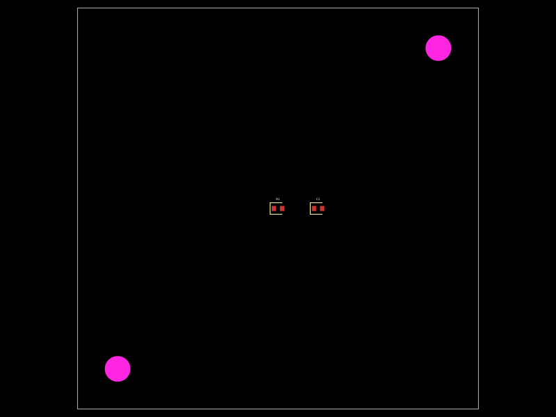 More from this authortechmannih/duplicate-NPTHA 50mm x 50mm PCB layout featuring two mounting holes, a 10kΩ resistor, and a 100nF capacitor positioned at specific coordinates.
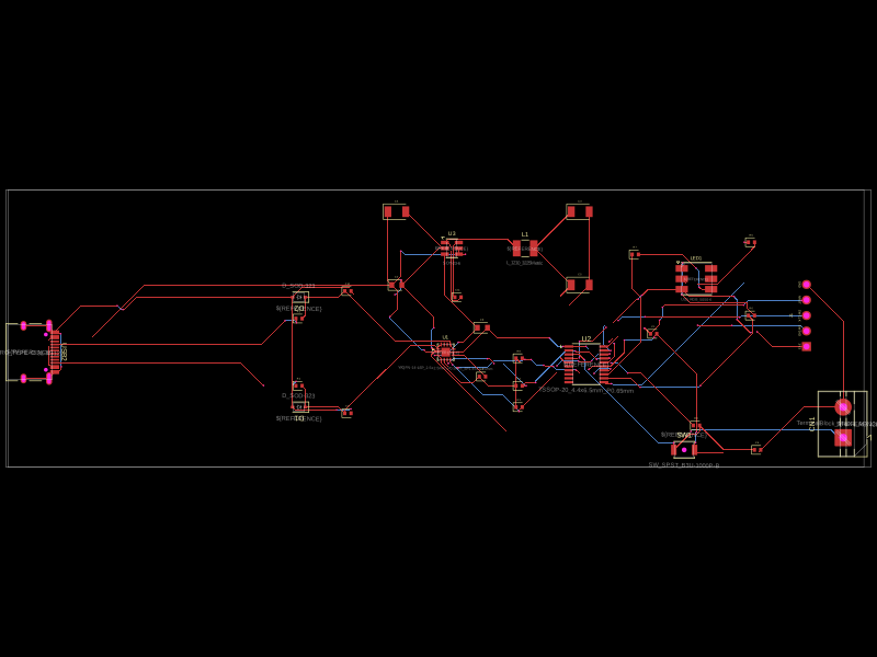 Similar packageaura/diy-power-delivery-triggerThis hardware design implements a USB Type-C port with supporting power management and signal conditioning components, including a USB-C connector, a FUSB302 USB-C port controller, ESD protection diodes, a buck converter for 3.3V power regulation, an STM32 microcontroller for control and processing, an RGB LED indicator, push button, terminal block connections, and associated filtering and support components.
 Discover something new0hmX/dual-usb-peltier-assembly