techmannih/museview
A 50×35 mm USB‑C 5 V camera board combining an ESP32‑S3 module, M0031 parallel camera connector, buck/LDO power rails, USB/ESD protection, controls, status LED, and passives.
- Version
- 0.1.18
- License
- unset
- Stars
- 1
docs/release-checks.md
# Release checks

Status: **NOT READY** for the first prototype. Only the two pre-order items below remain open; post-assembly measurements are listed separately. The machine-readable [`verification.json`](../release/verification.json) records the exact circuit hash and check outcomes. Manufacturing exports are versioned in `release/`, with SHA-256 hashes.

Local verification completed on 2026-10-05: source netlist, schematic placement, strict all-sheet Style Analysis, PCB placement, routing difficulty, board build, electrical contract, actual copper continuity, local bypasses, exact M0031 supply bounds, assembly/stock checks and separate Gerber short analysis passed. Twenty-nine regression tests passed, including supplier TVS pin polarity, the two captured renderer inputs and rejection of schematic style regressions. Native 2D and 3D snapshot regeneration/compare runs matched. The GitHub workflow repeats the circuit checks and 2D snapshots and compiles the matching ESP-IDF 5.4.2 firmware.

The 0.30 mm drill / 0.60 mm via pad revision includes regenerated routing, a native standard USB-C schematic and exact supplier pin-mapping checks. Four active copper layers are retained; see `routing.md` for the layer assessment. D1 imports the self-contained TVS drawing with its cathode bar toward VBUS_5V. All four sheets pass the pinned Style Analysis and missing-symbol rendering checks. No issue filters or disabled checks are used. The current routing fingerprint and drill tools are recorded in `release/verification.json`.

Exact trace/via counts are recorded in `verification.json`. There are zero build/routing errors and zero detected Gerber shorts. The retained native width warnings are explained in `electrical-review.md`; critical local widths are checked against their exact endpoints. All 28 selected assembly part numbers had positive JLCSearch stock in the dated evidence. This is availability evidence, not a PCBA order acceptance.

The handoff exporter verifies five KiCad schematic files (root plus four children) and all 16 distinct native/imported STEP models. GLB embeds the local OBJ bodies. KiCad files are interchange exports; no native KiCad ERC/DRC run is claimed. The tscircuit source and its checked copper remain authoritative.

| Check | Evidence required |
|---|---|
| Electrical contract | `bun run check:contract`, matches generated netlist |
| Stock | `sourcing/bom-with-stock.csv`, timestamped JLCSearch URLs |
| Type and source netlist | `bun run typecheck`, `tsci check netlist` |
| Placement and schematic | Native checks, strict `check:schematic-style` with zero issues, plus reviewed four-sheet renders |
| PCB | Zero build errors, connectivity checks, zero Gerber shorts |
| Bypass loops | `bun run check:decoupling`, actual local copper length |
| Assembly | Exact part identities, all fitted parts top, FPC pitch, JLC placement review |
| Firmware | CI compile and generated pin header consistency; physical operation separately |
| Fabrication | Review Gerber/drill/stackup/impedance with manufacturer |
| Hardware | Rails, startup, thermal/current/USB/camera tests in `bring-up.md` |

First-prototype blockers:

1. **Exact M0031-to-J2 mating qualification** — AFC01 requires a tighter 0.29–0.31 mm tail than F32R’s 0.27–0.33 mm range. Exact seating/latch fit remains unqualified. The numbered-tail photo also raises a possible reversed camera-to-J2 mapping after accounting for contact face and insertion direction; the current one-to-one numbering is not physically signed off. See `camera-mating.md`.
2. **JLC assembly placement approval** — the exported rotations are CAD angles. Verify U1/J1/J2/D1/LED1/U2/U3/U4/U5 alignment and centroids in the authenticated JLC preview, using `placement-review.md` and the generated `release/placement-review.json`. The Gerber upload was recognized as 4 layers, 50 × 35 mm. No order/payment was submitted.

After assembly: no physical PCB has been tested in this task. Source-current/inrush, rails/ripple/thermal behavior, USB enumeration and camera capture are prototype bring-up work before production. They are not circular prerequisites for ordering the first prototype. Manufacturing stackup and assembly eligibility must still match the actual quote; automated checks do not replace manufacturer review.

The 1.197 V camera-core revision is superseded. R8 = 25.5 kΩ and CAM_1V3 are mandatory. Electrical checks validate the declared board nets, including J2 pin 10 to CAM_1V3; they cannot prove the camera-to-connector contact mapping. See `camera-mating.md` for the tolerance comparison and possible numbering reversal. Neither exact tail qualification nor the numbered physical mating has been signed off.
Related Packages
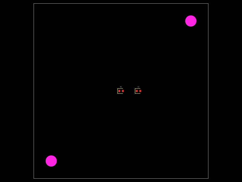 More from this authortechmannih/duplicate-NPTHA 50mm x 50mm PCB layout featuring two mounting holes, a 10kΩ resistor, and a 100nF capacitor positioned at specific coordinates.
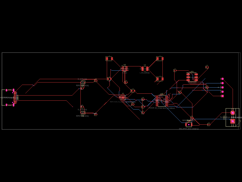 Similar packageaura/diy-power-delivery-triggerThis hardware design implements a USB Type-C port with supporting power management and signal conditioning components, including a USB-C connector, a FUSB302 USB-C port controller, ESD protection diodes, a buck converter for 3.3V power regulation, an STM32 microcontroller for control and processing, an RGB LED indicator, push button, terminal block connections, and associated filtering and support components.
 Discover something new0hmX/dual-usb-peltier-assembly