techmannih/museview
A 50×35 mm USB‑C 5 V camera board combining an ESP32‑S3 module, M0031 parallel camera connector, buck/LDO power rails, USB/ESD protection, controls, status LED, and passives.
- Version
- 0.1.18
- License
- unset
- Stars
- 1
docs/evidence/two-layer-feasibility.json
{
  "date": "2026-10-05",
  "status": "REJECTED_TWO_LAYER_TRIAL_NOT_FOR_ORDER",
  "baselineCommit": "7c9b41137d943b7360f18bac38ae7db58a59127b",
  "releaseDecision": "Retain existing four-layer hardware and release artifacts. Four layers are not a universal requirement.",
  "trialFileSha256": {
    "index.circuit.tsx": "7831cdb82c5045bb35e4d5c265d649945e9f9f10f0521cce32f847f5e8d3b5d4",
    "pcb-routes.json": "0b31679d36a51cbead71b4ae3327f213723ac2b1b874ab7521585a26d5f9b9b2",
    "routing/input.simple-route.json": "9e15d72eae2f5b334519e164809ab9830aa661e0ac51c5c65d74160370b09ccf",
    "routing/geometry.json": "8ea824c10d7bc068e3f0b4babd348ef91830a33a8d0560e8eda9f1b190e6b637",
    "scripts/route-grid.py": "68afb82fa60a9bb02444cfaa9c5e247543ac599f6573fad05963df410ea38989",
    "scripts/capture-routing-input.mjs": "751b35cda4104955b5dc56e65f625a4df59bd83c4ae9c701c0a2179b5e177dac",
    "scripts/analyze-ground-trial.mjs": "b1853a7204355f65b0df7458337719be71cd576ab662ba49124ba2f88b5e8272",
    "scripts/analyze-usb-return-trial.mjs": "9b1bd5d7d4c044fab397aa7c6db1ec84ee5fbdee399bad52cc82a02b58594eec",
    "dist/index/circuit.json": "9f2fe88b36141f4ceb80e1c52de21ea22f93a198618f32e1d3178af78738c0fe"
  },
  "boardLayers": 2,
  "generatedTraceCount": 120,
  "routerFailedConnections": [],
  "pcbTraceCount": 169,
  "pcbViaCount": 143,
  "nativeBuildExitCode": 1,
  "nativeErrors": [
    {
      "type": "pcb_port_not_connected_error",
      "message": "Port [J1.GND1] is not connected to net [GND] by a PCB trace."
    },
    {
      "type": "pcb_port_not_connected_error",
      "message": "Port [J1.GND2] is not connected to net [GND] by a PCB trace."
    },
    {
      "type": "pcb_port_not_connected_error",
      "message": "Port [R1.pin2] is not connected to net [GND] by a PCB trace."
    },
    {
      "type": "pcb_port_not_connected_error",
      "message": "Port [R2.pin2] is not connected to net [GND] by a PCB trace."
    },
    {
      "type": "pcb_port_not_connected_error",
      "message": "Port [R5.pin2] is not connected to net [GND] by a PCB trace."
    },
    {
      "type": "pcb_port_not_connected_error",
      "message": "Port [C1.pin2] is not connected to net [GND] by a PCB trace."
    },
    {
      "type": "pcb_port_not_connected_error",
      "message": "Port [U2.GND] is not connected to net [GND] by a PCB trace."
    },
    {
      "type": "pcb_port_not_connected_error",
      "message": "Port [D1.anode] is not connected to net [GND] by a PCB trace."
    },
    {
      "type": "pcb_port_not_connected_error",
      "message": "Port [R9.pin2] is not connected to net [GND] by a PCB trace."
    },
    {
      "type": "pcb_port_not_connected_error",
      "message": "Port [U1.GND1] is not connected to net [GND] by a PCB trace."
    },
    {
      "type": "pcb_port_not_connected_error",
      "message": "Port [U1.GND2] is not connected to net [GND] by a PCB trace."
    },
    {
      "type": "pcb_port_not_connected_error",
      "message": "Port [U1.GND3] is not connected to net [GND] by a PCB trace."
    },
    {
      "type": "pcb_port_not_connected_error",
      "message": "Port [SW1.B] is not connected to net [GND] by a PCB trace."
    },
    {
      "type": "pcb_port_not_connected_error",
      "message": "Port [SW1.D] is not connected to net [GND] by a PCB trace."
    },
    {
      "type": "pcb_port_not_connected_error",
      "message": "Port [SW2.B] is not connected to net [GND] by a PCB trace."
    },
    {
      "type": "pcb_port_not_connected_error",
      "message": "Port [SW2.D] is not connected to net [GND] by a PCB trace."
    },
    {
      "type": "pcb_port_not_connected_error",
      "message": "Port [SW3.B] is not connected to net [GND] by a PCB trace."
    },
    {
      "type": "pcb_port_not_connected_error",
      "message": "Port [SW3.D] is not connected to net [GND] by a PCB trace."
    },
    {
      "type": "pcb_port_not_connected_error",
      "message": "Port [LED1.cathode] is not connected to net [GND] by a PCB trace."
    },
    {
      "type": "pcb_port_not_connected_error",
      "message": "Port [J2.MP1] is not connected to net [GND] by a PCB trace."
    },
    {
      "type": "pcb_port_not_connected_error",
      "message": "Port [J2.MP2] is not connected to net [GND] by a PCB trace."
    },
    {
      "type": "pcb_port_not_connected_error",
      "message": "Port [R16.pin2] is not connected to net [GND] by a PCB trace."
    },
    {
      "type": "pcb_port_not_connected_error",
      "message": "Port [TP4.pin1] is not connected to net [GND] by a PCB trace."
    }
  ],
  "groundConnectivity": {
    "method": "Physical intersection/containment of GND pad, plated-hole, via, trace and pour polygons on common layers; no hypothetical added stitches included.",
    "groupCount": 3,
    "groups": [
      {
        "ports": [
          "J1.GND1",
          "J1.GND2",
          "R1.pin2",
          "R2.pin2",
          "R5.pin2",
          "C1.pin2",
          "U2.GND",
          "C18.pin2",
          "D1.anode",
          "U3.GND",
          "C2.pin2",
          "C3.pin2",
          "C4.pin2",
          "R7.pin2",
          "U4.VSS",
          "C6.pin2",
          "C7.pin2",
          "U5.GND",
          "C8.pin2",
          "C9.pin2",
          "R9.pin2",
          "U1.GND1",
          "U1.GND2",
          "U1.GND3",
          "U1.pin41_internal_1",
          "U1.pin41_internal_2",
          "U1.pin41_internal_3",
          "U1.pin41_internal_4",
          "U1.pin41_internal_5",
          "U1.pin41_internal_6",
          "U1.pin41_internal_7",
          "U1.pin41_internal_8",
          "C10.pin2",
          "C11.pin2",
          "C12.pin2",
          "SW1.B",
          "SW1.D",
          "SW2.B",
          "SW2.D",
          "SW3.B",
          "SW3.D",
          "LED1.cathode",
          "J2.MP1",
          "J2.MP2",
          "J2.AGND",
          "R16.pin2",
          "C14.pin2",
          "C15.pin2",
          "C17.pin2",
          "TP4.pin1"
        ],
        "geometryElementCount": 116
      },
      {
        "ports": [
          "C13.pin2",
          "C16.pin2"
        ],
        "geometryElementCount": 14
      },
      {
        "ports": [
          "J2.DGND"
        ],
        "geometryElementCount": 5
      }
    ],
    "limitations": "Geometric diagnostic, not electrical measurement or RF simulation; element areas overlap and are not reported as copper coverage."
  },
  "usbReferenceSampling": {
    "method": "0.05 mm centerline samples against actual opposite-layer GND pours/pads; includes connector/IC escape regions; not an impedance or field simulation",
    "report": [
      {
        "net": "USB_DM_PORT",
        "totalLengthMm": 21.65516587723596,
        "withoutOppositeGroundMm": 13.25225382605463,
        "longestGapMm": 3.6892869570040348
      },
      {
        "net": "USB_DP_PORT",
        "totalLengthMm": 19.832300500333798,
        "withoutOppositeGroundMm": 13.288838624274097,
        "longestGapMm": 2.963155729559737
      },
      {
        "net": "USB_DM_ESD",
        "totalLengthMm": 21.65516587723596,
        "withoutOppositeGroundMm": 13.25225382605463,
        "longestGapMm": 3.6892869570040348
      },
      {
        "net": "USB_DP_ESD",
        "totalLengthMm": 19.832300500333798,
        "withoutOppositeGroundMm": 13.288838624274097,
        "longestGapMm": 2.963155729559737
      },
      {
        "net": "USB_DM_MCU",
        "totalLengthMm": 1.9481982148521975,
        "withoutOppositeGroundMm": 1.9481982148521975,
        "longestGapMm": 1.9481982148521975
      },
      {
        "net": "USB_DP_MCU",
        "totalLengthMm": 1.9530275692762984,
        "withoutOppositeGroundMm": 0,
        "longestGapMm": 0
      }
    ]
  },
  "usbSamplingLimitations": "PORT/ESD aliases describe the same connected copper. Do not sum those rows. Ground traces/vias are not counted as a reference plane. No impedance qualification.",
  "releaseExported": false,
  "unchangedOrderBlockers": [
    "Exact M0031/AFC01 mechanical qualification",
    "Authenticated JLC placement-preview review"
  ]
}
Related Packages
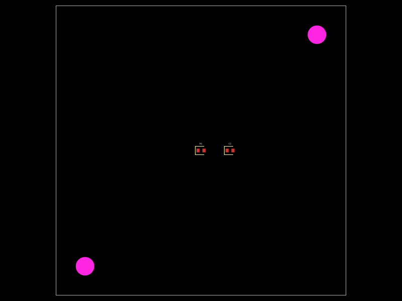 More from this authortechmannih/duplicate-NPTHA 50mm x 50mm PCB layout featuring two mounting holes, a 10kΩ resistor, and a 100nF capacitor positioned at specific coordinates.
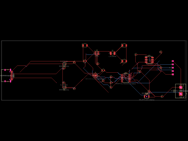 Similar packageaura/diy-power-delivery-triggerThis hardware design implements a USB Type-C port with supporting power management and signal conditioning components, including a USB-C connector, a FUSB302 USB-C port controller, ESD protection diodes, a buck converter for 3.3V power regulation, an STM32 microcontroller for control and processing, an RGB LED indicator, push button, terminal block connections, and associated filtering and support components.
 Discover something new0hmX/dual-usb-peltier-assembly