techmannih/footprint-check-placement
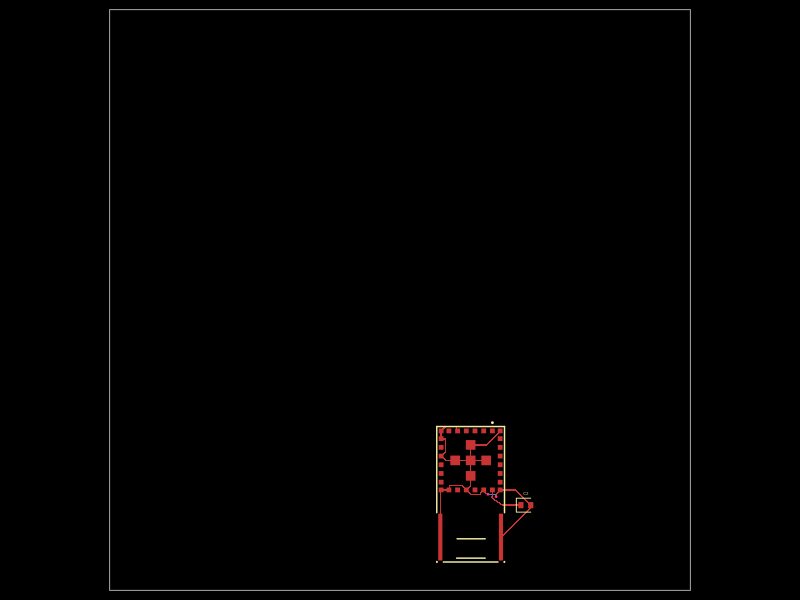
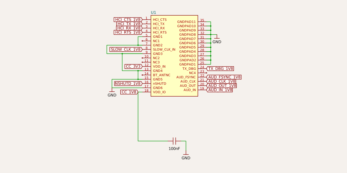
This design features a 10mm x 10mm PCB with an integrated clock module chip connected to various digital, audio, and power nets, along with a nearby 100nF surface-mount capacitor for decoupling.
- Version
- 0.0.1
- License
- unset
- Stars
- 0
index.tsx
PCB
Schematic
export default () => (
  <board width="60mm" height="60mm">
      <chip
      name="U1"
      schSheetName="module_clock"
      footprint="jlcpcb:C1526234"
      pcbX={7.3}
      pcbY={-20.1}
      pcbRotation={-90}
      schX={8}
      schY={1}
      connections={{
        HCI_CTS: "net.HCI_CTS_1V8",
        HCI_TX: "net.HCI_TX_1V8",
        HCI_RX: "net.HCI_RX_1V8",
        HCI_RTS: "net.HCI_RTS_1V8",
        GND1: "net.GND",
        GND2: "net.GND",
        SLOW_CLK_IN: "net.SLOW_CLK_1V8",
        GND3: "net.GND",
        VDD_IN: "net.CC_3V3",
        GND4: "net.GND",
        GND5: "net.GND",
        nSHUTD: "net.NSHUTD_1V8",
        GND6: "net.GND",
        VDD_IO: "net.CC_1V8",
        AUD_IN: "net.AUD_IN_1V8",
        AUD_OUT: "net.AUD_OUT_1V8",
        AUD_CLK: "net.AUD_CLK_1V8",
        AUD_FSYNC: "net.AUD_FSYNC_1V8",
        TX_DBG: "net.TX_DBG_1V8",
        GNDPAD1: "net.GND",
        GNDPAD2: "net.GND",
        GNDPAD3: "net.GND",
        GNDPAD4: "net.GND",
        GNDPAD5: "net.GND",
        GNDPAD6: "net.GND",
        GNDPAD7: "net.GND",
        GNDPAD8: "net.GND",
        GNDPAD9: "net.GND",
        GNDPAD10: "net.GND",
        GNDPAD11: "net.GND",
      }}
      noConnect={["NC1", "NC2", "NC3", "NC4", "BT_ANTNC"]}
    />
      <capacitor
      name="C2"
      schSheetName="module_clock"
      capacitance="100nF"
      footprint="cap0402"
      pcbX={13}
      pcbY={-21.2}
      schX={8}
      schY={-3}
      connections={{ pin1: "net.CC_1V8", pin2: "net.GND" }}
    />
  </board>
)