shibosoftwaredev/f1c100s-linux-nema17-stepper-controller
Compact four-layer NEMA 17 carrier PCB combining an F1C100S Linux SoC, USB-C PD power and buck regulation, W5500 10/100 Ethernet, STM32 safety/motion control, and DRV8825 stepper-driver hardware with protection, sensing, connectors, and dual-sided SMT assembly.
- Version
- 0.4.15
- License
- unset
- Stars
- 0
motor-stage.tsx
import { B4B_PH_K_S_LF__SN_ } from "./imports/B4B_PH_K_S_LF__SN_"
import { DRV8825PWPR } from "./imports/DRV8825PWPR"
import { HoLRT1206_1W_300mR_1_ } from "./imports/HoLRT1206_1W_300mR_1_"
import { PMEG6020ELRX } from "./imports/PMEG6020ELRX"
import { TCJD226M050R0090E } from "./imports/TCJD226M050R0090E"
import { TMP102AIDRLR } from "./imports/TMP102AIDRLR"

const signal = { thickness: 0.15 } as const
const ground = { thickness: 0.3 } as const
const power = { thickness: 0.8 } as const
// Request 0.30 mm phase copper; the router may neck locally at the driver's
// 0.65 mm-pitch pins. The protected motor-input path uses 0.80 mm copper.
const motor = { thickness: 0.3 } as const

const connect = (name: string, from: string, to: string, thickness = 0.15) =>
  <trace name={name} from={from} to={to} thickness={thickness} />

/**
 * A 15 V USB-PD, 0.40 A-peak stage for StepperOnline 17HS13-0404S1 NEMA 17.
 * A dedicated STM32 generates STEP/DIR. The enable line drives nRESET and
 * nSLEEP and is pulled down, so the bridge cannot energize during either CPU's
 * reset or before the USB-PD power-good interlock closes.
 */
export function MotorStage() {
  return <group name="MOTOR_STAGE" pcbX={0} pcbY={0} schX={-45} schY={0} schSheetName="motor_stage">
    <net name="VMOTOR" nominalTraceWidth={0.8} />
    <net name="DRV_VREF" nominalTraceWidth={0.15} />

    <fuse name="F_VM" layer="top" currentRating="2A" voltageRating="30V" footprint="1812"
      supplierPartNumbers={{jlcpcb:["C960026"]}} manufacturerPartNumber="BSMD1812-200-30V"
      pcbX={27.3} pcbY={11.3} schX={46} schY={12} schRotation={-90} />
    <PMEG6020ELRX name="D_VM_BLOCK" layer="top" pcbX={9.3} pcbY={-3.0} pcbRotation={180}
      schX={49} schY={12} schRotation={90} />
    <chip name="D_VM_TVS" layer="top" footprint="smb" pcbX={40} pcbY={12.2} pcbRotation={180}
      pinLabels={{pin1:"TVS1",pin2:"TVS2"}}
      supplierPartNumbers={{jlcpcb:["C1975329"]}} manufacturerPartNumber="SMBJ22CAQ-13-F"
      schX={49} schY={8} schPinArrangement={{topSide:[1],bottomSide:[2]}} />
    <TCJD226M050R0090E name="C_VM_BULK" layer="top" pcbX={42} pcbY={2} pcbRotation={90}
      schX={52} schY={8} schOrientation="vertical" />
    <capacitor name="C_VM_CER" layer="top" capacitance="10uF" maxVoltageRating="50V" footprint="1206"
      supplierPartNumbers={{jlcpcb:["C13585"]}} manufacturerPartNumber="CL31A106KBHNNNE"
      pcbX={34} pcbY={8.5} pcbRotation={180} schX={54} schY={8} schOrientation="vertical"
      maxDecouplingTraceLength={40} />

    <DRV8825PWPR name="U_MOTOR" layer="top" noConnect={["DECAY","nHOME","NC"]}
      pcbX={1.2} pcbY={-11.5} pcbRotation={0} schX={43} schY={0} schWidth={2.045} schHeight={2.94}
      schPinArrangement={{
        leftSide:{pins:[22,20,16,17,18,21,24,25,26],direction:"top-to-bottom"},
        rightSide:{pins:[5,7,10,8,6,9,19,27,23],direction:"top-to-bottom"},
        topSide:{pins:[4,1,15,2,11,3],direction:"left-to-right"},
        bottomSide:{pins:[12,13,14,28,29],direction:"left-to-right"},
      }} />

    {/* Charge pump, motor-rail bypassing, current regulation and safe defaults. */}
    <capacitor name="C_CP" layer="top" capacitance="10nF" maxVoltageRating="50V" footprint="0402"
      supplierPartNumbers={{jlcpcb:["C15195"]}} pcbX={-3.2} pcbY={-16.1}
      schX={43.4} schY={6} schRotation={90} maxDecouplingTraceLength={25} />
    <capacitor name="C_VCP" layer="top" capacitance="100nF" maxVoltageRating="50V" footprint="0402"
      supplierPartNumbers={{jlcpcb:["C960916"]}} pcbX={-3.22} pcbY={-17.33}
      schX={42} schY={6} schRotation={90} maxDecouplingTraceLength={25} />
    <resistor name="R_VCP" layer="bottom" resistance="1M" footprint="0402"
      supplierPartNumbers={{jlcpcb:["C26083"]}} pcbX={-4.5} pcbY={-17.8}
      schX={45} schY={6} schRotation={90} />
    <capacitor name="C_VMA" layer="top" capacitance="100nF" maxVoltageRating="50V" footprint="0402"
      supplierPartNumbers={{jlcpcb:["C960916"]}} pcbX={-1.3} pcbY={-16.1}
      schX={50} schY={6} schRotation={-90} maxDecouplingTraceLength={25} />
    <capacitor name="C_VMB" layer="top" capacitance="100nF" maxVoltageRating="50V" footprint="0402"
      supplierPartNumbers={{jlcpcb:["C960916"]}} pcbX={3.985} pcbY={-16.1}
      schX={52} schY={6} schRotation={-90} maxDecouplingTraceLength={25} />
    <capacitor name="C_DRV_3V3" layer="top" capacitance="470nF" maxVoltageRating="16V" footprint="0402"
      supplierPartNumbers={{jlcpcb:["C480644"]}} pcbX={40.5} pcbY={-4}
      schX={39} schY={-7} schRotation={-90} maxDecouplingTraceLength={25} />
    <resistor name="R_REF_TOP" layer="top" resistance="9.1k" footprint="0402"
      supplierPartNumbers={{jlcpcb:["C25742"]}} pcbX={8} pcbY={-14.8}
      schX={42} schY={-7} schRotation={90} />
    <resistor name="R_REF_BOTTOM" layer="top" resistance="2k" footprint="0402"
      supplierPartNumbers={{jlcpcb:["C4109"]}} pcbX={8} pcbY={-16.5}
      schX={45} schY={-7} schRotation={-90} />
    <capacitor name="C_REF" layer="top" capacitance="100nF" maxVoltageRating="16V" footprint="0402"
      supplierPartNumbers={{jlcpcb:["C1525"]}} pcbX={6} pcbY={-16.5}
      schX={48} schY={-7} schRotation={-90} maxDecouplingTraceLength={25} />
    <resistor name="R_ENABLE_PD" layer="top" resistance="100k" footprint="0402"
      supplierPartNumbers={{jlcpcb:["C25741"]}} pcbX={10.7} pcbY={-16.4}
      schX={37} schY={-3} schRotation={-90} />
    <resistor name="R_FAULT_PU" layer="top" resistance="10k" footprint="0402"
      supplierPartNumbers={{jlcpcb:["C25744"]}} pcbX={-2.5} pcbY={-6.8} schX={37} schY={-5} />
    {/* At 0.40 A/phase each 300 mOhm shunt dissipates only 48 mW. Placing
        them on the motor-side face frees the outward face for the RJ45. */}
    <HoLRT1206_1W_300mR_1_ name="R_ISEN_A" layer="bottom" pcbX={5.8} pcbY={-10.5} pcbRotation={90}
      schX={51} schY={-4} schOrientation="vertical" />
    <HoLRT1206_1W_300mR_1_ name="R_ISEN_B" layer="bottom" pcbX={8.7} pcbY={-10.5} pcbRotation={90}
      schX={54} schY={-4} schOrientation="vertical" />

    <B4B_PH_K_S_LF__SN_ name="J_MOTOR" layer="top" allowOffBoard pcbX={3} pcbY={-19.5} pcbRotation={0}
      schX={55} schY={0} />

    {/* TMP102 measures the driver-area board temperature; ALERT is read by PE6. */}
    <TMP102AIDRLR name="U_TEMP" layer="top" pcbX={12.0} pcbY={-19.0} pcbRotation={0}
      schX={43} schY={-10.5} />
    <capacitor name="C_TEMP" layer="top" capacitance="100nF" maxVoltageRating="16V" footprint="0402"
      supplierPartNumbers={{jlcpcb:["C1525"]}} pcbX={9.5} pcbY={-20.3}
      schX={47} schY={-10.5} schOrientation="vertical" maxDecouplingTraceLength={25} />
    <resistor name="R_TEMP_ALERT" layer="top" resistance="10k" footprint="0402"
      supplierPartNumbers={{jlcpcb:["C25744"]}} pcbX={9.2} pcbY={-18.0}
      schX={39} schY={-10.5} schOrientation="vertical" />

    {/* USB-PD input protection and local motor-energy storage. */}
    {connect("VM_INPUT", ".Q_VBUS > .pin8", ".F_VM > .pin1", 0.8)}
    <trace name="VM_FUSED" from=".F_VM > .pin2" to=".D_VM_BLOCK > .anode"
      thickness={power.thickness} pcbStraightLine />
    {connect("VM_PROTECTED", ".D_VM_BLOCK > .cathode", "net.VMOTOR", power.thickness)}
    {connect("VM_TVS", ".D_VM_TVS > .pin1", "net.VMOTOR", 0.8)}
    {connect("VM_TVS_GND", ".D_VM_TVS > .pin2", "net.BOARD_GND", 0.8)}
    {connect("VM_BULK", ".C_VM_BULK > .pin1", "net.VMOTOR", 0.8)}
    {connect("VM_BULK_GND", ".C_VM_BULK > .pin2", "net.BOARD_GND", 0.8)}
    {connect("VM_CER", ".C_VM_CER > .pin1", "net.VMOTOR", 0.8)}
    {connect("VM_CER_GND", ".C_VM_CER > .pin2", "net.BOARD_GND", 0.8)}

    {/* DRV8825 supply and charge pump. */}
    {connect("DRV_VMA", ".U_MOTOR > .VMA", "net.VMOTOR", 0.8)}
    {connect("DRV_VMB", ".U_MOTOR > .VMB", "net.VMOTOR", 0.8)}
    <trace name="DRV_C_VMA" from=".C_VMA > .pin1" to=".U_MOTOR > .VMA" thickness={0.3} pcbStraightLine />
    {connect("DRV_C_VMA_GND", ".C_VMA > .pin2", "net.BOARD_GND", 0.3)}
    <trace name="DRV_C_VMB" from=".C_VMB > .pin1" to=".U_MOTOR > .VMB" thickness={0.3} pcbStraightLine />
    {connect("DRV_C_VMB_GND", ".C_VMB > .pin2", "net.BOARD_GND", 0.3)}
    {connect("DRV_CP1", ".U_MOTOR > .CP1", ".C_CP > .pin1")}
    {connect("DRV_CP2", ".U_MOTOR > .CP2", ".C_CP > .pin2")}
    <trace name="DRV_VCP" from=".U_MOTOR > .VCP" to=".C_VCP > .pin1"
      thickness={0.12} pcbStraightLine />
    {connect("DRV_VCP_RETURN", ".C_VCP > .pin2", "net.VMOTOR")}
    <trace name="DRV_VCP_PULL" from=".R_VCP > .pin1" to=".C_VCP > .pin1" thickness={0.12}
      pcbPath={[
        ".R_VCP > .pin1",
        {x:-0.51,y:-0.62}, {x:6.49,y:-0.62}, {x:6.49,y:1.25},
        ".C_VCP > .pin1",
      ]} />
    {connect("DRV_VCP_PULL_RETURN", ".R_VCP > .pin2", "net.VMOTOR")}

    {/* 0.397 A peak/phase: 0.595 V reference and 0.30 ohm sense resistors. */}
    {connect("DRV_3V3_BYPASS", ".U_MOTOR > .V3P3OUT", ".C_DRV_3V3 > .pin1", 0.12)}
    {connect("DRV_3V3_GND", ".C_DRV_3V3 > .pin2", "net.BOARD_GND")}
    {connect("DRV_REF_FEED", ".U_MOTOR > .V3P3OUT", ".R_REF_TOP > .pin1", 0.12)}
    {connect("DRV_REF_DIV", ".R_REF_TOP > .pin2", "net.DRV_VREF")}
    {connect("DRV_REF_BOTTOM", ".R_REF_BOTTOM > .pin1", "net.DRV_VREF")}
    {connect("DRV_REF_GND", ".R_REF_BOTTOM > .pin2", "net.BOARD_GND")}
    {connect("DRV_REF_CAP", ".C_REF > .pin1", "net.DRV_VREF")}
    {connect("DRV_REF_CAP_GND", ".C_REF > .pin2", "net.BOARD_GND")}
    {connect("DRV_AVREF", ".U_MOTOR > .AVREF", "net.DRV_VREF")}
    {connect("DRV_BVREF", ".U_MOTOR > .BVREF", "net.DRV_VREF")}
    {connect("DRV_ISEN_A", ".U_MOTOR > .ISENA", ".R_ISEN_A > .pin1", 0.12)}
    {connect("DRV_ISEN_A_GND", ".R_ISEN_A > .pin2", "net.BOARD_GND", 0.4)}
    {connect("DRV_ISEN_B", ".U_MOTOR > .ISENB", ".R_ISEN_B > .pin1", 0.12)}
    {connect("DRV_ISEN_B_GND", ".R_ISEN_B > .pin2", "net.BOARD_GND", 0.4)}

    {/* Dedicated motion-MCU control. 1/16 microstep mode is fixed in hardware. */}
    {connect("TRACE_MOTOR_STEP", ".U_MOTOR > .STEP", "net.MOTOR_STEP")}
    {connect("TRACE_MOTOR_DIR", ".U_MOTOR > .DIR", "net.MOTOR_DIR")}
    {connect("MOTOR_SLEEP", ".U_MOTOR > .nSLEEP", "net.MOTOR_ENABLE")}
    {connect("MOTOR_RESET", ".U_MOTOR > .nRESET", "net.MOTOR_ENABLE")}
    {connect("MOTOR_ENABLE_PULLDOWN", ".R_ENABLE_PD > .pin1", "net.MOTOR_ENABLE")}
    {connect("MOTOR_ENABLE_PULLDOWN_GND", ".R_ENABLE_PD > .pin2", "net.BOARD_GND")}
    <trace name="TRACE_MOTOR_FAULT" from=".U_MOTOR > .nFAULT" to=".R_FAULT_PU > .pin1"
      thickness={signal.thickness}
      pcbPath={[".U_MOTOR > .nFAULT", {x:2.275,y:5.5}, {x:5.49,y:5.5}, ".R_FAULT_PU > .pin1"]} />
    {connect("MOTOR_FAULT_PULLUP", ".R_FAULT_PU > .pin1", "net.MOTOR_FAULT")}
    {connect("MOTOR_FAULT_PULLUP_3V3", ".R_FAULT_PU > .pin2", ".U_MOTOR > .MODE2")}
    <trace name="DRV_ENABLE_ACTIVE" from=".U_MOTOR > .nENBL" to=".U_MOTOR > .pin29"
      pcbPath={[".U_MOTOR > .nENBL",{x:0.325,y:1.4},{x:0,y:1.4},".U_MOTOR > .pin29"]} />
    <trace name="DRV_MODE0" from=".U_MOTOR > .MODE0" to=".U_MOTOR > .pin29"
      pcbPath={[".U_MOTOR > .MODE0",{x:-1.625,y:1.4},{x:0,y:1.4},".U_MOTOR > .pin29"]} />
    <trace name="DRV_MODE1" from=".U_MOTOR > .MODE1" to=".U_MOTOR > .pin29"
      pcbPath={[".U_MOTOR > .MODE1",{x:-2.275,y:1.4},{x:0,y:1.4},".U_MOTOR > .pin29"]} />
    {connect("DRV_GND1", ".U_MOTOR > .GND1", "net.BOARD_GND", 0.3)}
    {connect("DRV_GND2", ".U_MOTOR > .GND2", "net.BOARD_GND", 0.3)}
    {connect("DRV_EP_GND", ".U_MOTOR > .EP", "net.BOARD_GND", 0.8)}

    {/* Motor phases. */}
    {connect("MOTOR_A_PLUS", ".U_MOTOR > .AOUT1", ".J_MOTOR > .pin4", motor.thickness)}
    {connect("MOTOR_A_MINUS", ".U_MOTOR > .AOUT2", ".J_MOTOR > .pin3", motor.thickness)}
    <trace name="MOTOR_B_PLUS" from=".U_MOTOR > .BOUT1" to=".J_MOTOR > .pin1" thickness={motor.thickness}
      pcbPath={[".U_MOTOR > .BOUT1",
        {x:1.625,y:-4}, {x:1.1,y:-4.4},
        {x:1.1,y:-5.4}, {x:1.1,y:-5.4,via:true,fromLayer:"top",toLayer:"bottom"}, {x:1.1,y:-5.4},
        {x:5,y:-6}, {x:5,y:-17}, ".J_MOTOR > .pin1"]} />
    <trace name="MOTOR_B_MINUS" from=".U_MOTOR > .BOUT2" to=".J_MOTOR > .pin2" thickness={motor.thickness}
      pcbPath={[".U_MOTOR > .BOUT2",
        {x:0.325,y:-5}, {x:0.325,y:-5,via:true,fromLayer:"top",toLayer:"inner2"}, {x:0.325,y:-5},
        {x:-0.5,y:-6.2}, {x:0.8,y:-7.5}, {x:0.8,y:-17}, ".J_MOTOR > .pin2"]} />

    {/* Temperature monitor on the dedicated motion MCU's I2C bus. */}
    {connect("TEMP_VDD", ".U_TEMP > .V_POS", ".R_FAULT_PU > .pin2")}
    {connect("TEMP_GND", ".U_TEMP > .GND", "net.BOARD_GND", 0.3)}
    <trace name="TEMP_ADDR" from=".U_TEMP > .ADD0" to=".C_TEMP > .pin2" thickness={0.12}
      pcbPath={[
        ".U_TEMP > .ADD0", {x:-1.5,y:0.5}, {x:-1.5,y:-1.0},
        {x:1.91,y:-1.0}, ".C_TEMP > .pin2",
      ]} />
    {connect("TEMP_SDA", ".U_TEMP > .SDA", "net.MOTION_I2C_SDA")}
    {connect("TEMP_SCL", ".U_TEMP > .SCL", "net.MOTION_I2C_SCL")}
    {connect("TEMP_ALERT", ".U_TEMP > .ALERT", "net.MOTION_TEMP_ALERT")}
    {connect("TEMP_ALERT_PULLUP", ".R_TEMP_ALERT > .pin1", "net.MOTION_TEMP_ALERT")}
    {connect("TEMP_ALERT_PULLUP_3V3", ".R_TEMP_ALERT > .pin2", ".U_TEMP > .V_POS")}
    <trace name="TEMP_BYPASS" from=".U_TEMP > .V_POS" to=".C_TEMP > .pin1" thickness={0.12}
      pcbPath={[
        ".U_TEMP > .V_POS", {x:-1.8,y:0}, {x:-1.8,y:-1.5},
        {x:0.89,y:-1.5}, ".C_TEMP > .pin1",
      ]} />
    {connect("TEMP_BYPASS_GND", ".C_TEMP > .pin2", "net.BOARD_GND")}

    <silkscreentext text="A+  A-  B-  B+" pcbX={3} pcbY={-18.2} fontSize={0.65} />
    <silkscreentext text="NEMA17 / 0.40A / 1-16" pcbX={12} pcbY={-17.5} fontSize={0.6} />
  </group>
}
Related Packages
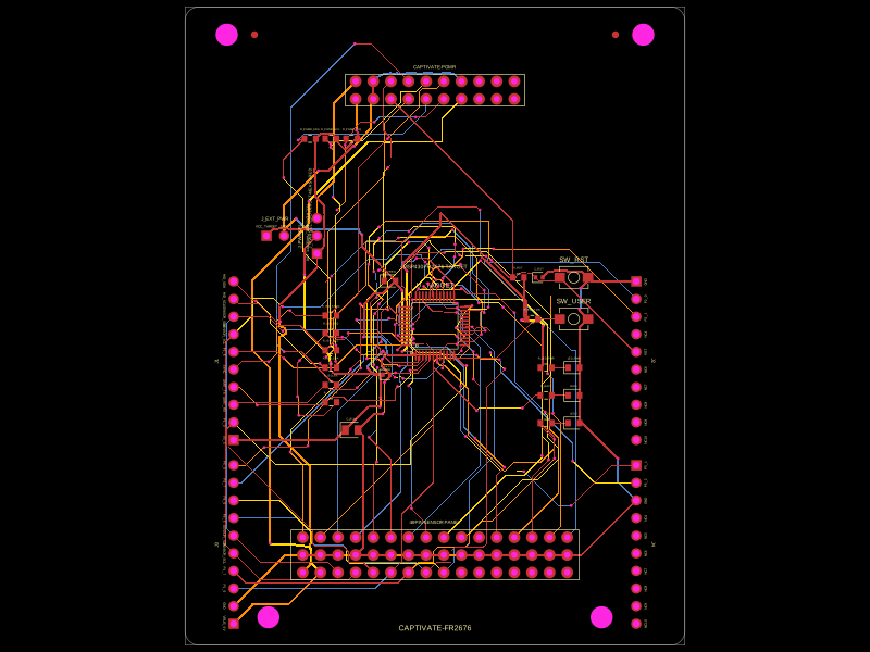 More from this authorShiboSoftwareDev/captivate-fr2676This circuit implements an MSP430FR2676 microcontroller-based development module with integrated power regulation, user interface components, programming interfaces, and sensor/boosterpack headers for embedded system prototyping.
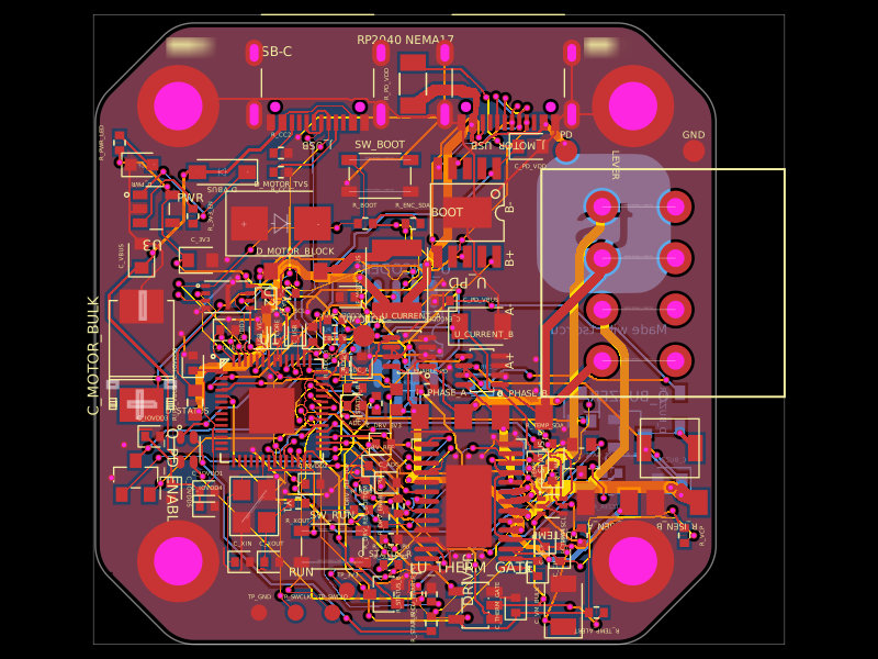 Similar packageastra/nema17-stepper-motor-controller-spring-clamp-rp2040A 4-layer RP2040 controller board that negotiates USB‑C PD motor power and drives a NEMA17 stepper via a DRV8825, with current sensing, thermal shutdown, RGB status LED, buzzer alarm, optional AS5600 encoder, protection/filtering, and test points.
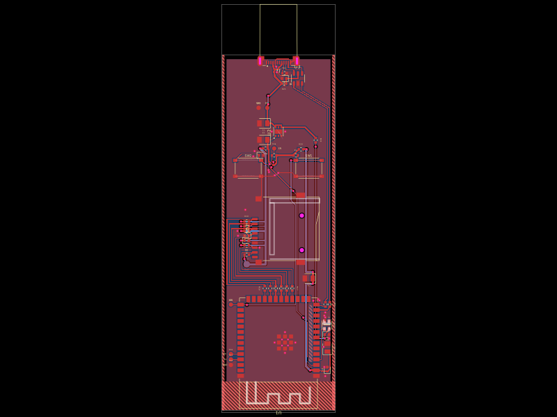 Discover something newpixalynx/esp32-usb-duckyA compact ESP32‑S3 USB‑C stick with native USB HID, 4‑bit microSD storage, 3.3V LDO power regulation, ESD protection, boot/reset controls, addressable RGB status LED, decoupling, and test pads.