shibosoftwaredev/f1c100s-linux-nema17-stepper-controller
Compact four-layer NEMA 17 carrier PCB combining an F1C100S Linux SoC, USB-C PD power and buck regulation, W5500 10/100 Ethernet, STM32 safety/motion control, and DRV8825 stepper-driver hardware with protection, sensing, connectors, and dual-sided SMT assembly.
- Version
- 0.4.15
- License
- unset
- Stars
- 0
modules/f1c100s/src/saved-paths.tsx
import type { FanoutTracePath } from "@tscircuit/props";
import type {
	GenericLocalAutorouter,
	SimpleRouteJson,
	Subcircuit,
} from "tscircuit";
import type { LayoutProfile } from "./profiles";
import native from "./generated/native.trace-paths.json";
import lcdTopStorageRight from "./generated/lcd_top_storage_right.trace-paths.json";
import lcdRightStorageBottom from "./generated/lcd_right_storage_bottom.trace-paths.json";
import lcdTopStorageBottom from "./generated/lcd_top_storage_bottom.trace-paths.json";
import lcdRightStorageLeft from "./generated/lcd_right_storage_left.trace-paths.json";
const profiles = {
	native,
	lcd_top_storage_right: lcdTopStorageRight,
	lcd_right_storage_bottom: lcdRightStorageBottom,
	lcd_top_storage_bottom: lcdTopStorageBottom,
	lcd_right_storage_left: lcdRightStorageLeft,
};

const rootsWithPlatedLayerAccess = new WeakSet<object>();

/** The source board used 0.35 mm via lands in three especially dense fanout
 * junctions.  Expanding every land to the requested 0.45 mm requires spreading
 * those junctions so JLCPCB's 0.10 mm copper gap remains intact. */
function preparePaths(paths: FanoutTracePath[], moveNorthSupportToBottom = false): FanoutTracePath[] {
	const prepared = structuredClone(paths) as FanoutTracePath[];
	const moves = [
		{ from: [3.4, -9.25], to: [3.525, -9.15] },
		{ from: [3.65, -9.05], to: [3.525, -9.15] },
		{ from: [9.6, 2.8], to: [9.75, 2.675] },
		{ from: [9.9, 2.55], to: [9.75, 2.675] },
		// Collapse this original shared ground stitch at a clear point.  The
		// 0.45 mm barrel then clears SDMMC0_D{0,1,3} and the SPI0 escape while
		// its adjacent top/inner2 segments retain more than 0.10 mm spacing.
		{ from: [9.2, 0.2], to: [9, 1.4] },
		{ from: [9.2, 2.4], to: [9, 1.4] },
		// Keep the top-layer branch east of C_OSCO after leaving the stitch.
		{ from: [9.2, 1.735], to: [10.2, 1.4] },
		{ from: [9.225, 1.71], to: [12.2, 1.4] },
		{ from: [9.225, 2.485], to: [10.2, 1.4] },
		{ from: [2.35, 9.4], to: [2.475, 9.3] },
		{ from: [2.6, 9.2], to: [2.475, 9.3] },
		// The recessed USB2 receptacle now occupies the original north-west
		// ground escape. Keep that shared stitch below its contact row.
		{ from: [-7.05, 9.5], to: [-10.2, 8.0] },
		{ from: [-7.4, 8.65], to: [-10.0, 7.0] },
		{ from: [-7.4, 8.2875], to: [-10.0, 6.5] },
		// Every duplicated ground tree must follow the relocated AVCC bypass
		// pad, not only the path whose endpoint is that capacitor.
		{ from: [-6.7125, 7.6], to: [-5.4125, 6.9] },
		// The north-going inner2 ground trunk ran through the western USB-C
		// shell drill after the module was placed on the compact carrier. Bend
		// the entire shared trunk east before it reaches the connector.
		{ from: [-5.0, 10.7], to: [-4.48, 10.7] },
	] as const;
	for (const path of prepared)
		for (const [index, point] of (path.route as any[]).entries()) {
			// Component-pad and breakout endpoints are immutable.
			if (index === 0 || index === path.route.length - 1) continue;
			const move = moves.find(
				({ from }) =>
					Math.abs(point.x - from[0]) < 1e-5 &&
					Math.abs(point.y - from[1]) < 1e-5,
			);
			if (move) [point.x, point.y] = move.to;
		}
	// Both ends of this old excursion are already on inner2. Removing the two
	// vias and intervening top copper creates a direct inner2 segment, safely
	// underneath the connector instead of between its shell holes and pads.
	for (const path of prepared) {
		const route = path.route as any[];
		const a = route.findIndex((p) => p.route_type === "via" && Math.abs(p.x + 6.4) < 1e-5 && Math.abs(p.y - 10.45) < 1e-5);
		const b = route.findIndex((p) => p.route_type === "via" && Math.abs(p.x + 4.0) < 1e-5 && Math.abs(p.y - 11.65) < 1e-5);
		if (a >= 0 && b >= 0) {
			const first = Math.min(a, b);
			const last = Math.max(a, b);
			path.route = [...route.slice(0, first), ...route.slice(last + 1)] as any;
		}
	}
	// The direct inner2 replacement must also bend around both USB2 shell
	// drills. Move its western junction below the connector, then approach the
	// eastern junction from the connector's open east side.
	for (const path of prepared) {
		const route = path.route as any[];
		for (const point of route) {
			if (point.route_type === "wire" && point.layer === "inner2" &&
				Math.abs(point.x + 6.4) < 1e-5 &&
				(Math.abs(point.y - 10.45) < 1e-5 || Math.abs(point.y - 10.15) < 1e-5)) {
				point.x = -2.0;
				point.y = 8.0;
			}
		}
		for (let index = 1; index < route.length; index++) {
			const previous = route[index - 1];
			const point = route[index];
			if (previous.route_type === "wire" && previous.layer === "inner2" &&
				point.route_type === "wire" && point.layer === "inner2" &&
				Math.abs(previous.x + 2.0) < 1e-5 && Math.abs(previous.y - 8.0) < 1e-5 &&
				Math.abs(point.x + 4.0) < 1e-5 && Math.abs(point.y - 11.65) < 1e-5) {
				route.splice(index, 0, { ...point, x: -2.5, y: 11.65 });
				break;
			}
		}
	}
	if (moveNorthSupportToBottom) {
		const placements: Record<string, { old: [number, number]; next: [number, number]; layer: "top" | "bottom" }> = {
			C_B_AVCC: { old: [-5.8, 7.6], next: [-4.5, 6.9], layer: "top" },
			C_B_VCC_DRAM: { old: [-6.2, -8.7], next: [-7.8, -8.9], layer: "bottom" },
			C_VRA2: { old: [-4.0, 10.45], next: [-5.4, 7.0], layer: "bottom" },
			R_VRA2: { old: [-7.6, 10.45], next: [-7.6, 7.0], layer: "bottom" },
			C_B_VCC_TV: { old: [9.15, 8.1], next: [7.8, 7.6], layer: "bottom" },
			C_TV_REF: { old: [9.2, 10.6], next: [7.2, 10.6], layer: "bottom" },
			R_PU_SPI0_CS: { old: [-10.7, -10.45], next: [-10.7, -7.0], layer: "bottom" },
		};
		for (const path of prepared) {
			const componentName = path.connection.split(".")[0]!;
			const placement = placements[componentName];
			if (!placement || !path.route.length) continue;
			const originalStart = path.route[0] as any;
			const dx = placement.next[0] - placement.old[0];
			const dy = placement.next[1] - placement.old[1];
			const start = { x: originalStart.x + dx, y: originalStart.y + dy };
			const wire = (x: number, y: number, layer: string) => ({
				route_type: "wire", x, y, width: originalStart.width, layer,
			});
			const via = (x: number, y: number, toLayer: string) => ({
				route_type: "via", x, y, from_layer: "bottom", to_layer: toLayer,
				via_diameter: 0.45, via_hole_diameter: 0.3,
			});
			const joinIndex = (x: number, y: number, layer: string) =>
				(path.route as any[]).findIndex((p) => p.route_type === "wire" && p.layer === layer && Math.abs(p.x - x) < 1e-5 && Math.abs(p.y - y) < 1e-5);
			const spliceBottom = (dogbone: [number, number], join: [number, number], layer: string) => {
				const index = joinIndex(join[0], join[1], layer);
				if (index < 0) throw new Error(`Missing ${path.connection} splice point ${join.join(",")}/${layer}`);
				path.route = [
					{ ...originalStart, ...start, layer: "bottom" },
					wire(dogbone[0], dogbone[1], "bottom"),
					via(dogbone[0], dogbone[1], layer),
					wire(dogbone[0], dogbone[1], layer),
					wire(join[0], join[1], layer),
					...(path.route as any[]).slice(index + 1),
				] as any;
			};
			const spliceOnBottom = (join: [number, number]) => {
				const index = joinIndex(join[0], join[1], "bottom");
				if (index < 0) throw new Error(`Missing ${path.connection} bottom splice point`);
				path.route = [
					{ ...originalStart, ...start, layer: "bottom" },
					wire(join[0], join[1], "bottom"),
					...(path.route as any[]).slice(index + 1),
				] as any;
			};

			// Splice the relocated support parts directly into the first useful
			// layer of their proven native fanout. This avoids carrying obsolete
			// top-side endpoint tails through either recessed USB-C footprint.
			if (path.connection === "C_B_AVCC.pin1") {
				const index = joinIndex(-4.55, 7.95, "top");
				path.route = [
					{ ...originalStart, ...start, layer: "top" },
					wire(start.x, 7.95, "top"),
					wire(-4.55, 7.95, "top"),
					...(path.route as any[]).slice(index + 1),
				] as any;
				continue;
			}
			if (path.connection === "C_B_AVCC.pin2") {
				const index = joinIndex(-5.0, 6.35, "inner2");
				path.route = [
					{ ...originalStart, ...start, layer: "top" },
					wire(-4.7, 6.9, "top"),
					wire(-4.7, 4.8, "top"),
					{ ...via(-4.7, 4.8, "inner2"), from_layer: "top" },
					wire(-4.7, 4.8, "inner2"),
					wire(-5.0, 6.35, "inner2"),
					...(path.route as any[]).slice(index + 1),
				] as any;
				continue;
			}
			if (path.connection === "C_B_VCC_DRAM.pin2") {
				spliceBottom([start.x, start.y - 1.3], [-9.6, -7.65], "inner1");
				continue;
			}
			if (path.connection === "C_B_VCC_DRAM.pin1") {
				const dogbone: [number, number] = [start.x + 0.25, start.y + 0.75];
				path.route = [
					{ ...originalStart, ...start, layer: "bottom" },
					wire(dogbone[0], dogbone[1], "bottom"),
					via(dogbone[0], dogbone[1], "top"),
					wire(dogbone[0], dogbone[1], "top"),
					{ ...originalStart, layer: "top" },
					...(path.route as any[]).slice(1),
				] as any;
				continue;
			}
			if (path.connection === "C_VRA2.pin1") {
				spliceBottom([-5.4, 5.8], [-2.2, 7.45], "inner1");
				continue;
			}
			if (path.connection === "C_VRA2.pin2") {
				spliceBottom([-6.15, start.y], [-5.0, 6.35], "inner2");
				continue;
			}
			if (path.connection === "R_VRA2.pin1") {
				const index = joinIndex(-2.2, 7.45, "inner1");
				path.route = [
					{ ...originalStart, ...start, layer: "bottom" },
					wire(-9.2, 3.5, "bottom"),
					via(-9.2, 3.5, "inner1"),
					wire(-9.2, 3.5, "inner1"),
					wire(-7.8, 3.4, "inner1"),
					wire(-3.5, 3.6, "inner1"),
					wire(-3.0, 5.5, "inner1"),
					wire(-2.2, 7.45, "inner1"),
					...(path.route as any[]).slice(index + 1),
				] as any;
				continue;
			}
			if (path.connection === "R_VRA2.pin2") {
				spliceBottom([-6.34, start.y], [-5.0, 6.35], "inner2");
				continue;
			}
			if (path.connection === "C_B_VCC_TV.pin1") {
				spliceOnBottom([7.55, 7.05]);
				continue;
			}
			if (path.connection === "C_B_VCC_TV.pin2") {
				spliceOnBottom([10.75, 9.15]);
				continue;
			}
			if (path.connection === "C_TV_REF.pin1") {
				spliceBottom([start.x, 9.85], [7.45, 9.3], "inner2");
				continue;
			}
			if (path.connection === "C_TV_REF.pin2") {
				spliceBottom([start.x, 11.35], [10.8, 11.65], "inner2");
				continue;
			}
			if (placement.layer === "top") {
				path.route = [
					{ ...originalStart, ...start, layer: "top" },
					{ ...originalStart, layer: "top" },
					...path.route.slice(1),
				] as any;
				continue;
			}
			const radial = { x: start.x - placement.next[0], y: start.y - placement.next[1] };
			const length = Math.hypot(radial.x, radial.y) || 1;
			const dogbone = componentName === "R_PU_SPI0_CS" ? {
				x: start.x,
				y: start.y - 0.75,
			} : componentName === "C_B_VCC_DRAM" ? {
				x: start.x,
				y: start.y + 0.75,
			} : {
				x: start.x + 0.75 * radial.x / length,
				y: start.y + 0.75 * radial.y / length,
			};
			path.route = [
				{ ...originalStart, ...start, layer: "bottom" },
				{ route_type: "wire", ...dogbone, width: originalStart.width, layer: "bottom" },
				{ route_type: "via", ...dogbone, from_layer: "bottom", to_layer: "top", via_diameter: 0.45, via_hole_diameter: 0.3 },
				{ route_type: "wire", ...dogbone, width: originalStart.width, layer: "top" },
				{ ...originalStart, layer: "top" },
				...path.route.slice(1),
			] as any;
		}
	}
	return prepared;
}

/** The pinned core drops pcb_port.layers when making router input. Restore
 * layer access from actual plated-hole obstacles immediately before routing,
 * for both saved fanouts and the carrier's configured local autorouter. */
function preservePlatedLayerAccess(
	instance: Subcircuit,
	savedPaths: FanoutTracePath[],
) {
	const root = instance.root!;
	if (rootsWithPlatedLayerAccess.has(root)) return;
	rootsWithPlatedLayerAccess.add(root);
	root.on(
		"autorouting:start",
		({ simpleRouteJson: input }: { simpleRouteJson: SimpleRouteJson }) => {
			if (!input) return;
			// The stored fanout belongs to this nested subcircuit. Core excludes
			// nested traces from the parent board phase by default, which allowed
			// carrier routes to cross the already-fabricated SoC escape copper.
			// When a parent connection is being routed, preload every saved fanout
			// trace as an immutable obstacle. Reusing the original IDs lets the
			// phase output update rather than duplicate the physical trace records.
			const isParentRouting = input.connections.some((connection) => {
				const sourceTraceId = connection.source_trace_id ??
					(connection.name?.startsWith("source_trace_") ? connection.name : undefined);
				const sourceTrace = sourceTraceId
					? root.db.source_trace.get(sourceTraceId)
					: undefined;
				return sourceTrace && sourceTrace.subcircuit_id !== instance.subcircuit_id;
			});
			if (isParentRouting) {
				// The fanout primitives render after the parent board autorouter, so
				// they are not yet present in circuit JSON. Preload their exact saved
				// geometry here as synthetic immutable traces. The carrier's fixed
				// router strips these obstacle-only IDs from its final output; the
				// module fanout itself emits the real copper in its later phase.
				const transform = instance._computePcbGlobalTransformBeforeLayout();
				const existingIds = new Set(
					(input.traces ?? []).map((trace) => trace.pcb_trace_id),
				);
				for (const [index, path] of savedPaths.entries()) {
					const pcbTraceId = `saved_fanout_obstacle_${index}`;
					if (existingIds.has(pcbTraceId)) continue;
					input.traces ??= [];
					input.traces.push({
						type: "pcb_trace",
						pcb_trace_id: pcbTraceId,
						source_trace_id: pcbTraceId,
						connection_name: pcbTraceId,
						connectsTo: [],
						route: path.route.map((point: any) => ({
							...point,
							x: transform.a * point.x + transform.c * point.y + transform.e,
							y: transform.b * point.x + transform.d * point.y + transform.f,
							...(point.route_type === "via" ? {
								via_diameter: 0.45,
								via_hole_diameter: 0.3,
							} : {}),
						})),
					} as any);
					existingIds.add(pcbTraceId);
				}
			}
			for (const connection of input.connections)
				for (const point of connection.pointsToConnect) {
					const hole = input.obstacles.find(
						(o) =>
							o.circuitJsonMetadata?.pcb_plated_hole_id &&
							Math.hypot(o.center.x - point.x, o.center.y - point.y) < 1e-5 &&
							(o.circuitJsonMetadata.pcb_port_id === point.pcb_port_id ||
								o.connectedTo.includes(
									connection.source_trace_id ?? connection.name,
								)),
					);
					if (hole) point.layers = [...hole.layers] as any;
				}
		},
	);
}

/** Every saved path on a net ends at the same junction. This final phase checks
 * that invariant; it never solves or invents copper. Parent routing is separate. */
export async function joinSavedPathExits(
	input: SimpleRouteJson,
): Promise<GenericLocalAutorouter> {
	for (const connection of input.connections) {
		const points = connection.pointsToConnect,
			first = points[0];
		// Core's SRJ currently defaults a physical port to its first layer.
		// A real plated barrel joins coincident exits on different layers.
		const barrel =
			first &&
			input.obstacles.find(
				(o) =>
					o.circuitJsonMetadata?.pcb_plated_hole_id &&
					Math.hypot(o.center.x - first.x, o.center.y - first.y) < 1e-4 &&
					o.connectedTo.some(
						(id) =>
							id === connection.name ||
							id === connection.source_trace_id ||
							points.some((p) => p.pcb_port_id === id),
					) &&
					points.every((p) =>
						(p.layers ?? [p.layer]).some((l) => o.layers.includes(l)),
					),
			);
		if (
			first &&
			points.some(
				(p) =>
					Math.hypot(p.x - first.x, p.y - first.y) > 1e-4 ||
					(!barrel &&
						!(p.layers ?? [p.layer]).some((l) =>
							(first.layers ?? [first.layer]).includes(l),
						)),
			)
		) {
			throw new Error(`Saved F1C100S paths do not meet for ${connection.name}`);
		}
	}
	const listeners: Record<string, ((event: any) => void)[]> = {
		complete: [],
		error: [],
		progress: [],
	};
	return {
		input,
		isRouting: false,
		on(event, listener) {
			listeners[event]!.push(listener);
		},
		start() {
			queueMicrotask(() =>
				listeners.complete!.forEach((f) => f({ type: "complete", traces: [] })),
			);
		},
		stop() {},
		solveSync() {
			return [];
		},
	};
}

/** Use the native saved-fanout API for copper, retaining the imported footprint
 * and schematic symbols. Electrical traces remain outside the fanout. */
export function attachSavedPaths(
	instance: Subcircuit,
	profile: LayoutProfile,
	paths?: FanoutTracePath[],
) {
	const preparedPaths = preparePaths(
		paths ?? profiles[profile] as FanoutTracePath[],
		profile === "native",
	);
	preservePlatedLayerAccess(instance, preparedPaths);
	(instance as any)._isInflatedFromCircuitJson = false;
	const check = instance.doInitialPcbDesignRuleChecks.bind(instance);
	instance.doInitialPcbDesignRuleChecks = () => {
		deduplicateSharedVias(instance);
		check();
	};
	const module = instance.selectOne(".MODULE") as any;
	const components = [...module.children];
	module.add(
		<fanout
			name="COPPER"
			pcbX={0}
			pcbY={0}
			schLayout={{ layoutMode: "relative" }}
			pcbTracePaths={preparedPaths}
		/>,
	);
	const fanout = module.selectOne(".COPPER");
	fanout._doInitialSchematicLayoutSections = () => {};
	for (const component of components) {
		module.children = module.children.filter((c: any) => c !== component);
		fanout.add(component);
	}
	for (const trace of instance.selectAll("trace") as any[]) {
		for (const props of [trace.props, trace._parsedProps]) {
			delete props.pcbPath;
			delete props.pcbStraightLine;
			props.maxLength = /^N_HOSC[IO]$/.test(props.name ?? "") ? 10 : 5000;
			if (/^N_HOSC[IO]$/.test(props.name ?? "")) props.maxViaCount = 0;
			props.path = props.path?.map((p: string) =>
				p.replace(".MODULE > ", ".MODULE .COPPER > "),
			);
		}
	}
}

/** Core currently emits a via for every path that shares it. Keep one physical
 * drill per same-net location before either native or independent DRC runs. */
function deduplicateSharedVias(instance: Subcircuit) {
	const db = instance.root!.db;
	const seen = new Map<string, string>();
	for (const via of db.pcb_via.list()) {
		if (via.subcircuit_id !== instance.subcircuit_id) continue;
		const key = [
			via.x.toFixed(6),
			via.y.toFixed(6),
			via.hole_diameter,
			via.outer_diameter,
			[...via.layers].sort().join(","),
		].join(":");
		const traceId = db.pcb_trace.get(via.pcb_trace_id!)?.source_trace_id;
		// Separate pin-to-cap traces can belong to one electrical supply net.
		const net =
			(traceId &&
				db.source_trace.get(traceId)?.subcircuit_connectivity_map_key) ??
			traceId ??
			"";
		if (seen.has(key)) {
			if (seen.get(key) !== net)
				throw new Error("Different nets share an F1C100S via");
			db.pcb_via.delete(via.pcb_via_id);
		} else seen.set(key, net);
	}
}
Related Packages
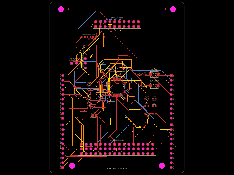 More from this authorShiboSoftwareDev/captivate-fr2676This circuit implements an MSP430FR2676 microcontroller-based development module with integrated power regulation, user interface components, programming interfaces, and sensor/boosterpack headers for embedded system prototyping.
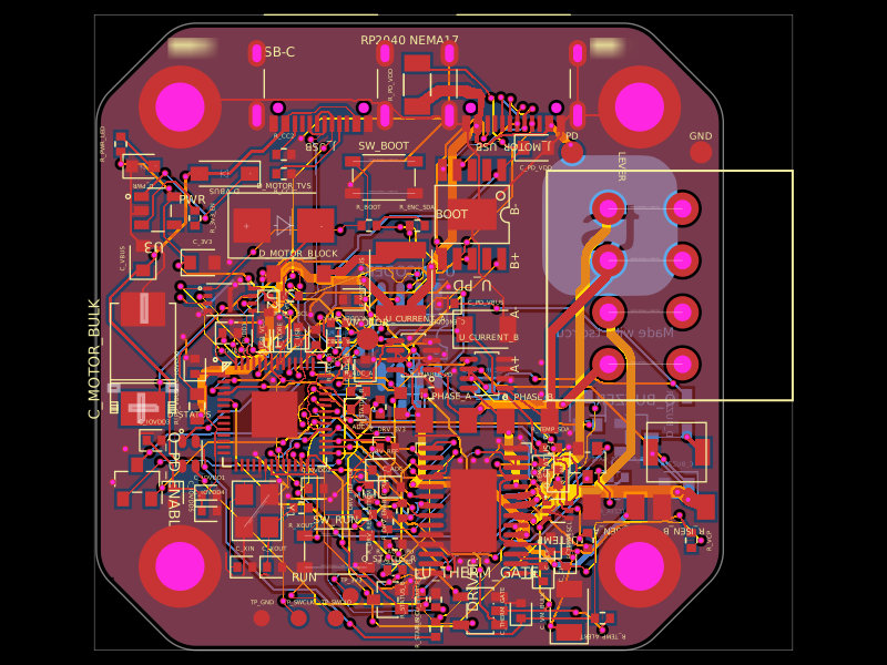 Similar packageastra/nema17-stepper-motor-controller-spring-clamp-rp2040A 4-layer RP2040 controller board that negotiates USB‑C PD motor power and drives a NEMA17 stepper via a DRV8825, with current sensing, thermal shutdown, RGB status LED, buzzer alarm, optional AS5600 encoder, protection/filtering, and test points.
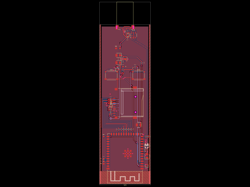 Discover something newpixalynx/esp32-usb-duckyA compact ESP32‑S3 USB‑C stick with native USB HID, 4‑bit microSD storage, 3.3V LDO power regulation, ESD protection, boot/reset controls, addressable RGB status LED, decoupling, and test pads.