shibosoftwaredev/f1c100s-linux-nema17-stepper-controller
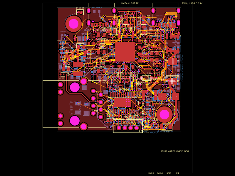
Compact four-layer NEMA 17 carrier PCB combining an F1C100S Linux SoC, USB-C PD power and buck regulation, W5500 10/100 Ethernet, STM32 safety/motion control, and DRV8825 stepper-driver hardware with protection, sensing, connectors, and dual-sided SMT assembly.
- Version
- 0.4.15
- License
- unset
- Stars
- 0
index.circuit.tsx
PCB
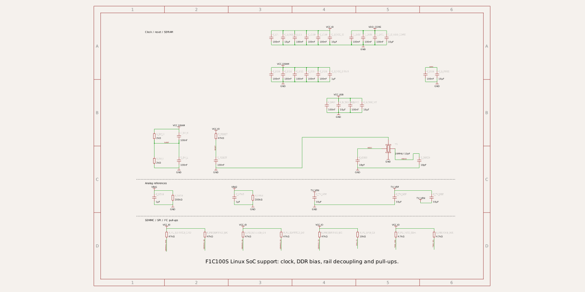
Schematic
import { Fragment } from "react"
import { footprints } from "./footprints"
import { MotorStage } from "./motor-stage"
import { PdPower, UsbPowerPort } from "./pd-power"
import { EthernetSection } from "./ethernet"
import { MotionController } from "./motion-controller"
import { routingBoundaryRef } from "./routing-boundary"
import {
  F1C100SModule,
  F1C100SLcdSchematicBox,
  F1C100SStorageSchematicBox,
  F1C100SGpioSchematicBox,
  F1C100SAudioSchematicBox,
  F1C100SVideoTouchSchematicBox,
  F1C100SSystemSchematicBox,
  F1C100SPowerSchematicBox,
} from "./modules/f1c100s/src"
import { ElectricalCorrections } from "./electrical-corrections"
import { nema17FixedRouter } from "./nema17-fixed-router"

// Keep the strict 42.3 mm motor-back square centered on the standard 31 mm
// diagonal NEMA 17 mounting pattern. Edge connectors are recessed far enough
// that every drilled feature and annulus is supported without outline tabs.
const nema17BoardCenter = { x: 0, y: 0 }
const nema17BoardOutline = [
  { x: -21.15, y: 21.15 },
  { x: 21.15, y: 21.15 },
  { x: 21.15, y: -21.15 },
  { x: -21.15, y: -21.15 },
] as const

// Four-layer carrier. The NEMA17-sized body carries the proven Linux module,
// PD, Ethernet and real-time motion section. The checked deterministic routes
// keep local and cloud builds identical.
const connect = (part: string, nets: string[]) => nets.map((net, i) =>
  net ? <Fragment key={`${part}-${i}`}><trace name={`${part}_PIN${i + 1}_CONNECTION`}
    from={`.${part} > .pin${i + 1}`}
    to={net.startsWith(".") || net.startsWith("net.") ? net : `net.${net}`} /></Fragment> : null)
const cap = (name: string, value: string, net: string, x: number, y: number, rotation = 0, target?: string, schX = x, schY = y, schSheetName?: string, layer: "top" | "bottom" = "bottom") => <>
  <capacitor name={name} layer={layer} capacitance={value} footprint={value === "4.7uF" ? "0805" : "0603"} maxVoltageRating={value === "4.7uF" ? 16 : undefined} manufacturerPartNumber={value === "4.7uF" ? "GRM21BR71C475KE51L" : undefined} pcbX={x} pcbY={y} pcbRotation={rotation} schX={schX} schY={schY} schRotation={-90} schSheetName={schSheetName} />
  <trace name={`${name}_SUPPLY`} from={`.${name} > .pin1`} to={target ?? `net.${net}`} maxLength={target ? 15 : undefined} />
  <trace name={`${name}_GROUND`} from={`.${name} > .pin2`} to="net.BOARD_GND" maxLength={1000} />
</>
const powerCapSchPosition: Record<string, { x: number; y: number }> = {
  C_U_2V5_IN: { x: 3.5, y: 4.5 },
  // U_1V2 and U_2V8 are stacked below U_2V5. Their input capacitors share
  // VCC_USB and remain vertically grouped on the regulators' left side.
  C_U_1V2_IN: { x: 1, y: -9.5 },
}

const ldoCap = (name: string, net: string, x: number, y: number, rotation: number, target: string,
  schX: number, schY: number) => <>
  <capacitor name={name} layer="bottom" capacitance="4.7uF" maxVoltageRating={16}
    footprint="0603" manufacturerPartNumber="CL10A475KO8NNNC"
    supplierPartNumbers={{jlcpcb:["C19666"]}}
    pcbX={x} pcbY={y} pcbRotation={rotation}
    schX={powerCapSchPosition[name]?.x ?? schX} schY={powerCapSchPosition[name]?.y ?? schY}
    schRotation={-90} schSheetName="power_rails" />
  <trace name={`${name}_SUPPLY`} from={`.${name} > .pin1`} to={target} maxLength={15} />
  <trace name={`${name}_GROUND`} from={`.${name} > .pin2`} to="net.BOARD_GND" maxLength={1000} />
</>
const resistor = (name: string, value: string, a: string, b: string, x: number, y: number, schX = x, schY = y, schSheetName?: string) => <>
  <resistor name={name} layer="bottom" resistance={value} footprint="0603" pcbX={x} pcbY={y} schX={schX} schY={schY} schSheetName={schSheetName} />
  {connect(name, [a, b])}
</>
const primaryLdo = (name: string, input: string, output: string, x: number, y: number, schX: number, schY: number) => <>
  <chip name={name} layer="bottom" manufacturerPartNumber="AP2112K-3.3TRG1"
    supplierPartNumbers={{jlcpcb:["C51118"]}}
    footprint="dfn6_missing(5)_p0.95mm_w3.5mm_pw0.5mm_pl0.9mm_pin1location(rightside,bottom)"
    pinLabels={{pin1:"IN",pin2:"GND",pin3:"EN",pin4:"NC",pin5:"OUT",pin6:"NC6",pin7:"NC7",pin8:"NC8"}}
    pinAttributes={{pin2:{requiresGround:true},pin4:{doNotConnect:true},pin6:{doNotConnect:true},pin7:{doNotConnect:true},pin8:{doNotConnect:true}}}
    pcbX={x} pcbY={y} schX={schX} schY={schY} schHeight={0.6} schSheetName="power_rails" />
  {/* Keep five connection records so the frozen carrier routing remains stable. */}
  <trace name={`${name}_OUTPUT`} from={`.${name} > .pin5`}
    to={output.startsWith(".") || output.startsWith("net.") ? output : `net.${output}`} />
  <trace name={`${name}_ENABLE`} from={`.${name} > .pin3`} to={`.C_${name}_IN > .pin1`} />
  <trace from={`.${name} > .pin2`} to="net.BOARD_GND" />
  <trace from={`.${name} > .pin2`} to="net.BOARD_GND" />
  <trace name={`${name}_INPUT`} from={`.${name} > .pin1`}
    to={input.startsWith(".") || input.startsWith("net.") ? input : `net.${input}`} />
  {cap(`C_${name}_IN`, "4.7uF", input, x+5.8, y+1.905, 0, `.${name} > .pin1`, schX+5, schY+1, "power_rails")}
  {cap(`C_${name}_OUT`, "4.7uF", output, x-5.8, y+1.905, 180, `.${name} > .pin5`, schX-5, schY-0.5, "power_rails")}
</>

type LdoPcbPlacement = {
  u: { x: number; y: number }
  inputCap: { x: number; y: number; rotation: number }
  outputCap: { x: number; y: number; rotation: number }
}

// AP2112K SOT-25: input 1, ground 2, enable 3, NC 4, output 5.
const ldoK = (name: string, voltage: string, output: string, x: number, y: number, schX: number, schY: number,
  mpn = `AP2112K-${voltage}TRG1`, input = "V3V3", placement?: LdoPcbPlacement) => <>
  <chip name={name} layer="bottom" manufacturerPartNumber={mpn}
    footprint="dfn6_missing(5)_p0.95mm_w3.5mm_pw0.5mm_pl0.9mm_pin1location(rightside,bottom)"
    pinLabels={{pin1:"IN",pin2:"GND",pin3:"EN",pin4:"NC",pin5:"OUT"}}
    pinAttributes={{pin2:{requiresGround:true},pin4:{doNotConnect:true}}}
    pcbX={placement?.u.x ?? x} pcbY={placement?.u.y ?? y} schX={schX} schY={schY} schHeight={0.6} schSheetName="power_rails" />
  <trace name={`${name}_INPUT`} from={`.${name} > .pin1`}
    to={input.startsWith(".") || input.startsWith("net.") ? input : `net.${input}`} />
  <trace name={`${name}_ENABLE`} from={`.${name} > .pin3`} to={`.${name} > .pin1`} />
  <trace name={`${name}_OUTPUT`} from={`.${name} > .pin5`} to={`net.${output}`} />
  {ldoCap(`C_${name}_IN`, input,
    placement?.inputCap.x ?? x+4.2, placement?.inputCap.y ?? y-0.95,
    placement?.inputCap.rotation ?? 0, `.${name} > .pin1`, schX-4, schY-1.5)}
  {ldoCap(`C_${name}_OUT`, output,
    placement?.outputCap.x ?? x-4.2, placement?.outputCap.y ?? y-0.95,
    placement?.outputCap.rotation ?? 180, `.${name} > .pin5`, schX+4, schY-1.5)}
  {/* Both ground pins land directly in the carrier ground system. The former
      generic pcbPath used fixed absolute coordinates and left the 1.2 V LDO
      branch disconnected after placement overrides moved the regulator. */}
  <trace name={`${name}_LOCAL_GND`} from={`.${name} > .pin2`} to="net.BOARD_GND" />
</>

export default () => <board outline={[...nema17BoardOutline]} layers={4}
  minTraceWidth={0.12} minViaPadDiameter={0.45} minViaHoleDiameter={0.3}
  pcbStyle={{viaPadDiameter:0.45, viaHoleDiameter:0.3}}
  isViaInPadAllowed
  autorouter="auto-local" autorouterEffortLevel="2x"
  {...{ref:routingBoundaryRef}} schLayout={{layoutMode:"relative"}} schTraceAutoLabelEnabled schMaxTraceDistance={3}>
  <autoroutingphase name="nema17-fabrication-routing" autorouter="auto-local"
    algorithmFn={nema17FixedRouter}
    minTraceToPadEdgeClearance={0.1} minPadEdgeToPadEdgeClearance={0.1}
    minViaEdgeToPadEdgeClearance={0.1} />
  {/* Keep each functional block readable on its own drawing. Components use
      schSheetName below; these declarations provide titles and sheet-local
      notes without changing PCB order or placement. */}
  <schematicsheet name="soc_support" displayName="1 — F1C100S support" sheetIndex={1} sheetSize="A4">
    <schematictext text="F1C100S Linux SoC support: clock, DDR bias, rail decoupling and pull-ups." schX={0} schY={-12.2} fontSize={0.42} />
  </schematicsheet>
  <schematicsheet name="linux_io" displayName="2 — Linux interfaces" sheetIndex={2} sheetSize="ANSI_B">
    <F1C100SSystemSchematicBox moduleName="SOC" schX={-14} schY={5} />
    <F1C100SStorageSchematicBox moduleName="SOC" schX={0} schY={5} />
    <F1C100SGpioSchematicBox moduleName="SOC" schX={14} schY={5} />
    <schematictext text="Boot flash, reset and USB2/FEL data interface. Ethernet and motion links continue by net label." schX={0} schY={-12.2} fontSize={0.42} />
  </schematicsheet>
  <schematicsheet name="soc_unused" displayName="3 — Unused SoC interfaces" sheetIndex={3} sheetSize="A4">
    <F1C100SLcdSchematicBox moduleName="SOC" schX={-8} schY={4.5} />
    <F1C100SAudioSchematicBox moduleName="SOC" schX={6} schY={4.5} />
    <F1C100SVideoTouchSchematicBox moduleName="SOC" schX={0} schY={-4.5} />
    <schematictext text="Unused F1C100S LCD, audio, video and touch pins are documented here; they are not external expansion headers." schX={0} schY={-12.2} fontSize={0.42} />
  </schematicsheet>
  <schematicsheet name="pd_power" displayName="4 — USB-C PD and 5 V" sheetIndex={4} sheetSize="ANSI_B">
    <schematictext text="Dedicated USB-C PD power input requests 15 V / 3 A. The separate USB-C data port is USB2/FEL only." schX={0} schY={-16.05} fontSize={0.42} />
  </schematicsheet>
  <schematicsheet name="power_rails" displayName="5 — SoC power rails" sheetIndex={5} sheetSize="A4">
    <F1C100SPowerSchematicBox moduleName="SOC" schX={-8} schY={4.5} />
    <schematictext text="Dedicated 3.3 V, 2.8 V, 2.5 V and 1.2 V rails. Regulator ratings are device limits, not a board load budget." schX={0} schY={-12.2} fontSize={0.42} />
  </schematicsheet>
  <schematicsheet name="ethernet" displayName="6 — 10/100 Ethernet" sheetIndex={6} sheetSize="ANSI_B">
    <schematictext text="W5500 Ethernet over SPI with integrated-magnetics RJ45 and reference termination network." schX={0} schY={-12.2} fontSize={0.42} />
  </schematicsheet>
  <schematicsheet name="motion" displayName="7 — Real-time stepper control" sheetIndex={7} sheetSize="ANSI_B">
    <schematictext text="STM32 watchdog motion controller. Linux sends commands over UART; the MCU owns STEP/DIR and the hardware-safe enable path." schX={0} schY={-13.2} fontSize={0.42} />
  </schematicsheet>
  <schematicsheet name="motor_stage" displayName="8 — NEMA 17 stepper driver" sheetIndex={8} sheetSize="ANSI_B">
    <schematictext text="DRV8825 power stage for StepperOnline 17HS13-0404S1: 15 V, 0.40 A peak/phase, fixed 1/16 microstep, protected USB-PD motor rail." schX={0} schY={-13.2} fontSize={0.42} />
  </schematicsheet>
  <net name="BOARD_GND" isGroundNet nominalTraceWidth={0.3} />
  <net name="PD_VDD" nominalTraceWidth={0.15} />
  {/* The fitted 0-ohm links below form one DC rail while keeping each physical
      branch short enough to route deterministically on the dense motor back. */}
  {/* The data connector is intentionally separated from the SoC-side USB
      nets by U_USB_ESD's feed-through pin pairs. */}
  <net name="USB_N_PORT" nominalTraceWidth={0.15} />
  <net name="USB_P_PORT" nominalTraceWidth={0.15} />
  <net name="V2V8" nominalTraceWidth={0.12} />
  <net name="V2V5" nominalTraceWidth={0.12} />
  <net name="V1V2" nominalTraceWidth={0.12} />

  <net name="ETH_CS" nominalTraceWidth={0.15} />
  <net name="ETH_MOSI" nominalTraceWidth={0.15} />
  <net name="ETH_SCLK_SOC" nominalTraceWidth={0.15} />
  <net name="ETH_MISO" nominalTraceWidth={0.15} />
  <net name="ETH_RST" nominalTraceWidth={0.15} />
  <net name="ETH_INT" nominalTraceWidth={0.15} />

  <net name="FLASH_CLK" nominalTraceWidth={0.15} />
  <net name="SOC_FLASH_CS" nominalTraceWidth={0.15} />
  <net name="FLASH_MOSI" nominalTraceWidth={0.15} />
  <net name="FLASH_MISO" nominalTraceWidth={0.15} />
  <net name="FLASH_CS" nominalTraceWidth={0.15} />
  <net name="FLASH_HOLD" nominalTraceWidth={0.15} />
  <net name="FLASH_WP" nominalTraceWidth={0.15} />

  <net name="MOTION_RX" nominalTraceWidth={0.15} />
  <net name="MOTION_TX" nominalTraceWidth={0.15} />
  <net name="MOTION_BOOT" nominalTraceWidth={0.15} />
  <net name="MOTION_NRST" nominalTraceWidth={0.15} />
  <net name="MOTOR_STEP" nominalTraceWidth={0.15} />
  <net name="MOTOR_DIR" nominalTraceWidth={0.15} />
  <net name="MOTOR_ENABLE_RAW" nominalTraceWidth={0.15} />
  <net name="MOTOR_ENABLE" nominalTraceWidth={0.15} />
  <net name="MOTOR_FAULT" nominalTraceWidth={0.15} />
  <net name="MOTION_TEMP_ALERT" nominalTraceWidth={0.15} />
  <net name="MOTION_I2C_SCL" nominalTraceWidth={0.15} />
  <net name="MOTION_I2C_SDA" nominalTraceWidth={0.15} />

  <net name="USB_N" nominalTraceWidth={0.15} />
  <net name="USB_P" nominalTraceWidth={0.15} />
  <net name="RESET_N" nominalTraceWidth={0.15} />
  <F1C100SModule name="SOC" layoutProfile="native" schematicLayout="custom"
    pcbX={2} pcbY={6} schX={0} schY={-2} schSheetName="soc_support"
    breakoutOffsets={{PE10:{x:0.5,y:2.4}}}
    connections={{
      GND:"net.BOARD_GND", VDD_CORE:"net.V1V2", VCC_DRAM:"net.V2V5",
      VCC_IO:".U_3V3 > .pin5", VCC_USB:".SOC .VCC_TV > .pin1", AVCC:"net.V2V8",
      VCC_HP:".SOC .VCC_IO > .pin1", VCC_TV:".R_V3V3_RIGHT > .pin2",
      SPI0_CLK:"net.FLASH_CLK", SPI0_CS:"net.SOC_FLASH_CS",
      SPI0_MOSI:"net.FLASH_MOSI", SPI0_MISO:"net.FLASH_MISO",
      PE7:"net.ETH_CS", PE8:"net.ETH_MOSI", PE9:"net.ETH_SCLK_SOC", PE10:"net.ETH_MISO",
      UART0_TX:"net.MOTION_RX", UART0_RX:"net.MOTION_TX",
      USB_DM:"net.USB_N", USB_DP:"net.USB_P", RESET:"net.RESET_N",
      PE2:"net.MOTION_BOOT", PE3:"net.MOTION_NRST",
      PE5:"net.ETH_RST", PE6:"net.ETH_INT",
    }} />

  <PdPower />
  <EthernetSection />
  <MotionController />
  <resistor name="R_ETH_SCLK" resistance="0" footprint="0201"
    layer="top" manufacturerPartNumber="RC0201JR-070RL"
    supplierPartNumbers={{jlcpcb:["C25079"]}} pcbX={7.0} pcbY={-5.5} pcbRotation={0}
    schX={8} schY={10} schSheetName="ethernet" />
  <trace name="ETH_SCLK_SOC_LINK" from=".R_ETH_SCLK > .pin2" to="net.ETH_SCLK_SOC" thickness={0.15} />
  <trace name="ETH_SCLK_DIRECT" from=".R_ETH_SCLK > .pin1" to=".U_ETH > .SCLK" thickness={0.15}
    pcbPath={[".R_ETH_SCLK > .pin1",
      {x:0.51,y:-0.62}, {x:0.51,y:-0.62,via:true,fromLayer:"bottom",toLayer:"inner2"},
      {x:0.51,y:12.28}, {x:-2.303266,y:12.28},
      {x:-2.303266,y:12.28,via:true,fromLayer:"inner2",toLayer:"bottom"},
      ".U_ETH > .SCLK"]} />
  {/* The HUSB238A open-drain contract-valid signal crosses the board on the
      bottom layer. Fixed vias keep the QFN escape away from adjacent VBUS. */}
  <trace name="PD_GOOD_REMOTE" from=".Q_PD_ENABLE > .G" to=".R_PD_GOOD_PU > .pin1" thickness={0.15}
    pcbPath={[".U_PD > .GATE",
      {x:-2.6,y:-0.25}, {x:-2.6,y:-0.25,via:true,fromLayer:"top",toLayer:"bottom"},
      {x:-2.6,y:-0.25},
      {x:-5.2,y:-4}, {x:-5.2,y:-8.3},
      {x:-5.6,y:-8.3}, {x:-5.6,y:-9.7}, {x:-5.2,y:-9.7},
      {x:-5.2,y:-12.5}, {x:-24.35,y:-31.7},
      {x:-34.18,y:-31.72}, {x:-34.18,y:-31.72,via:true,fromLayer:"bottom",toLayer:"top"},
      {x:-34.18,y:-31.72},
      {x:-37.15,y:-31.75}, ".Q_PD_ENABLE > .G"]} />

  {/* AP2112K SOT-25: output 1, ground 2, enable 3, input 5. */}
  {primaryLdo("U_3V3", ".R_BUCK_FF > .pin1", ".R_V3V3_RIGHT > .pin1", -21, 9, 5, 6)}
  <resistor name="R_V3V3_RIGHT" layer="bottom" resistance="0" footprint="0402"
    supplierPartNumbers={{jlcpcb:["C17168"]}} pcbX={14.2} pcbY={13.2}
    schX={13} schY={6} schRotation={-90} schSheetName="power_rails" />
  {/* Keep the W5500 supply feed a two-terminal route.  Without this fitted
      link, the right-side regulator rail forms a board-spanning MST whose
      Ethernet branch can be stranded by the dense SoC escape. */}
  <resistor name="R_V3V3_ETH" layer="top" resistance="0" footprint="0402"
    supplierPartNumbers={{jlcpcb:["C17168"]}} pcbX={15.0} pcbY={4.5}
    schX={13.33} schY={4.75} schRotation={-90} schSheetName="power_rails" />
  <trace name="V3V3_ETH_LINK_IN" from=".R_V3V3_ETH > .pin1" to=".R_V3V3_RIGHT > .pin2" thickness={0.2} />
  <trace name="V3V3_ETH_FEED_DIRECT" from=".R_V3V3_ETH > .pin2" to=".FB_ETH > .pin1" thickness={0.25}
    pcbPath={[
      ".R_V3V3_ETH > .pin2", {x:0.51,y:0.9}, {x:-2.3,y:0.9},
      {x:-2.3,y:0.9,via:true,fromLayer:"top",toLayer:"inner1"},
      {x:-0.3,y:0.9}, {x:-0.3,y:-29.6}, {x:-10.375,y:-29.6}, {x:-10.375,y:-28.35},
      {x:-10.375,y:-28.35,via:true,fromLayer:"inner1",toLayer:"bottom"},
      ".FB_ETH > .pin1",
    ]} />
  <resistor name="R_V3V3_MOTION" layer="bottom" resistance="0" footprint="0402"
    supplierPartNumbers={{jlcpcb:["C17168"]}} pcbX={-15} pcbY={-4}
    schX={12.68} schY={3.5} schRotation={-90} schSheetName="power_rails" />
  <trace name="V3V3_MOTION_LINK_IN" from=".R_V3V3_MOTION > .pin1" to=".R_V3V3_RIGHT > .pin1" thickness={0.2} />
  <trace name="V3V3_MOTION_LINK_OUT" from=".R_V3V3_MOTION > .pin2" to=".C_MOTION_BULK > .pin1" thickness={0.2} />
  <resistor name="R_V3V3_MOTOR" layer="bottom" resistance="0" footprint="0402"
    supplierPartNumbers={{jlcpcb:["C17168"]}} pcbX={-3.37} pcbY={-6.08}
    schX={13} schY={1} schRotation={-90} schSheetName="power_rails" />
  <trace name="V3V3_MOTOR_LINK_IN" from=".R_V3V3_MOTOR > .pin1" to=".R_V3V3_MOTION > .pin2" thickness={0.2} />
  <trace name="V3V3_MOTOR_LINK_OUT" from=".R_V3V3_MOTOR > .pin2" to=".U_MOTOR > .MODE2" thickness={0.2} />
  {ldoK("U_2V5", "2.5", "V2V5", -21, 0, 5, 1, "AP2112K-2.5TRG1", ".R_V3V3_RIGHT > .pin1", {
    u:{x:17.4,y:-4.25}, inputCap:{x:20.2,y:-5.8,rotation:90}, outputCap:{x:20.2,y:-2.7,rotation:90},
  })}
  {ldoK("U_1V2", "1.2", "V1V2", -21, -8, 5, -8, "AP2112K-1.2TRG1", ".SOC .VCC_TV > .pin1", {
    u:{x:17.4,y:1.95}, inputCap:{x:20.2,y:0.4,rotation:90}, outputCap:{x:20.2,y:3.5,rotation:90},
  })}
  {/* Codec AVCC requires 2.5–3.1 V; dedicated 2.8 V supply. */}
  {ldoK("U_2V8", "2.8", "V2V8", 43, 24, 5, -4, "TPAP2127K-2.8TRG1", ".U_1V2 > .pin1", {
    u:{x:17.4,y:8.15}, inputCap:{x:20.2,y:6.6,rotation:90}, outputCap:{x:20.2,y:9.7,rotation:90},
  })}

  {/* 16 MiB SPI NOR for SPL / U-Boot / compact Linux + rootfs. */}
  <chip name="U_FLASH" manufacturerPartNumber="W25Q128JVSIQ"
    layer="bottom" footprint={footprints.flash}
    pinLabels={{pin1:"CS_N",pin2:"DO",pin3:"WP_N",pin4:"BOARD_GND",pin5:"DI",pin6:"CLK",pin7:"HOLD_N",pin8:"VCC"}}
    pcbX={19.5} pcbY={7} schX={5} schY={-2} schSheetName="linux_io" />
  {connect("U_FLASH", ["FLASH_CS","FLASH_MISO","","BOARD_GND","FLASH_MOSI","FLASH_CLK","FLASH_HOLD",".U_2V5 > .pin1"])}
  {cap("C_FLASH", "100nF", "V3V3", 25.7, 8.905, 0, ".U_FLASH > .pin8", 10.33, -2, "linux_io")}
  <resistor name="R_WP" layer="bottom" resistance="10k" footprint="0402"
    supplierPartNumbers={{jlcpcb:["C25744"]}} pcbX={-20} pcbY={9}
    schX={10} schY={-5} schRotation={90} schSheetName="linux_io" />
  <trace name="FLASH_WP_PULLUP_SIGNAL" from=".R_WP > .pin1" to="net.FLASH_WP" />
  <trace name="FLASH_WP_PULLUP_SUPPLY" from=".R_WP > .pin2" to=".U_FLASH > .VCC" />
  <trace name="FLASH_WP_DIRECT" from=".U_FLASH > .WP_N" to=".R_WP > .pin1" thickness={0.15}
    pcbPath={[".U_FLASH > .WP_N",
      {x:-5,y:-0.635}, {x:-5,y:-0.635,via:true,fromLayer:"top",toLayer:"inner1"}, {x:-5,y:-0.635},
      {x:-5,y:-5.5}, {x:6.175,y:-5.5},
      {x:6.175,y:-5.5,via:true,fromLayer:"inner1",toLayer:"top"}, {x:6.175,y:-5.5},
      ".R_WP > .pin1"]} />
  <resistor name="R_HOLD" layer="bottom" resistance="10k" footprint="0402"
    supplierPartNumbers={{jlcpcb:["C25744"]}} pcbX={-20} pcbY={11}
    schX={9.68} schY={-3.5} schRotation={90} schSheetName="linux_io" />
  <trace name="FLASH_HOLD_PULLUP_SIGNAL" from=".R_HOLD > .pin1" to="net.FLASH_HOLD" />
  <trace name="FLASH_HOLD_PULLUP_SUPPLY" from=".R_HOLD > .pin2" to=".R_WP > .pin2" />
  <resistor name="R_FLASH_CS" layer="bottom" resistance="10k" footprint="0402"
    supplierPartNumbers={{jlcpcb:["C25744"]}} pcbX={-20} pcbY={13}
    schX={1} schY={-5} schRotation={90} schSheetName="linux_io" />
  <trace name="FLASH_CS_PULLUP_SIGNAL" from=".R_FLASH_CS > .pin1" to="net.FLASH_CS" />
  <trace name="FLASH_CS_PULLUP_SUPPLY" from=".R_FLASH_CS > .pin2" to=".R_HOLD > .pin2" />
  {/* Normally closed copper link: cut the narrow bridge to isolate SPI-flash
      CS and force F1C100S USB FEL recovery, then re-bridge with solder. This
      is a fabricated PCB feature, not an assembled header or BOM item. */}
  <solderjumper name="JP_BOOT" layer="top" bridged doNotPlace
    footprint="solderjumper2_p1.0_pw0.7_ph0.8"
    pinLabels={{pin1:"SOC_CS",pin2:"FLASH_CS"}}
    pcbX={-13.3} pcbY={19.45} schX={5} schY={-8} schSheetName="linux_io" />
  {connect("JP_BOOT", ["SOC_FLASH_CS","FLASH_CS"])}

  <chip name="SW_RESET" layer="top" footprint={<footprint>
      {/* Omron B3U-1000P datasheet land pattern: 4.2 mm outer span,
          2.6 mm inner span, and 1.7 mm pad height. */}
      <smtpad portHints={["pin1"]} pcbX={-1.7} pcbY={0} width={0.8} height={1.7} shape="rect" />
      <smtpad portHints={["pin2"]} pcbX={1.7} pcbY={0} width={0.8} height={1.7} shape="rect" />
      <courtyardrect pcbX={0} pcbY={0} width={4.5} height={3.2} />
    </footprint>}
    manufacturerPartNumber="B3U-1000P" supplierPartNumbers={{jlcpcb:["C231329"]}}
    pinLabels={{pin1:"RESET",pin2:"BOARD_GND"}}
    pcbX={-26.5} pcbY={15} schX={-13} schY={-5}
    schPinArrangement={{topSide:[1],bottomSide:[2]}}
    schSheetName="linux_io" />
  {connect("SW_RESET", ["RESET_N","BOARD_GND"])}
  {/* USBLC6-2P6: the same two-line USB2 protection network in the compact
      SOT-666 package; duplicate IO pads are internally common. */}
  <chip name="U_USB_ESD" layer="top" manufacturerPartNumber="USBLC6-2P6"
    supplierPartNumbers={{jlcpcb:["C15999"]}} footprint={<footprint>
      {/* ST DS4260 Figure 21: 0.30 x 0.62 mm lands, 0.50 mm pitch,
          0.99 mm row-center offset. */}
      <smtpad portHints={["pin1"]} pcbX={-0.99} pcbY={0.5} width={0.62} height={0.3} shape="rect" />
      <smtpad portHints={["pin2"]} pcbX={-0.99} pcbY={0} width={0.62} height={0.3} shape="rect" />
      <smtpad portHints={["pin3"]} pcbX={-0.99} pcbY={-0.5} width={0.62} height={0.3} shape="rect" />
      <smtpad portHints={["pin4"]} pcbX={0.99} pcbY={-0.5} width={0.62} height={0.3} shape="rect" />
      <smtpad portHints={["pin5"]} pcbX={0.99} pcbY={0} width={0.62} height={0.3} shape="rect" />
      <smtpad portHints={["pin6"]} pcbX={0.99} pcbY={0.5} width={0.62} height={0.3} shape="rect" />
      <courtyardrect pcbX={0} pcbY={0} width={2.9} height={2.1} />
    </footprint>}
    pinLabels={{pin1:"DM1",pin2:"BOARD_GND",pin3:"DP1",pin4:"DP2",pin5:"VBUS",pin6:"DM2"}}
    pcbX={-9.4} pcbY={11.3} pcbRotation={0} schX={-9} schY={-2} schSheetName="linux_io" />
  {connect("U_USB_ESD", ["USB_N_PORT","BOARD_GND","USB_P_PORT","USB_P",".SOC .VCC_TV > .pin1","USB_N"])}
  {cap("C_ESD", "100nF", "V3V3", -9.5, 8.8, 0, ".U_USB_ESD > .pin5", -4, -2, "linux_io", "top")}

  <MotorStage />
  {/* Render the new connector last so all established component/port IDs stay
      stable for the deterministic fabrication routing. */}
  <UsbPowerPort />
  {/* Added after the frozen carrier to preserve all established component and
      trace identifiers used by the deterministic board router. */}
  <ElectricalCorrections />

  {[[nema17BoardCenter.x-15.5,nema17BoardCenter.y+15.5],
    [nema17BoardCenter.x+15.5,nema17BoardCenter.y-15.5]].map(([x,y]) => {
    const index=(x>0?2:0)+(y>0?1:0)+1
    return <Fragment key={`${x}:${y}`}><chip name={`MH${index}`} doNotPlace noSchematicRepresentation pcbX={x} pcbY={y}
      footprint={<footprint><platedhole portHints={["pin1"]} shape="circle" holeDiameter="3.3mm" outerDiameter="5.6mm" /></footprint>}
      pinLabels={{pin1:"CHASSIS"}} noConnect={["CHASSIS"]} /></Fragment>
  })}
  <silkscreentext text="F1C100S LINUX / NEMA17 STEPPER" pcbX={nema17BoardCenter.x} pcbY={14} fontSize={0.7} />
  <silkscreentext text="42.3 mm / 31 mm MOUNT" layer="bottom" pcbX={nema17BoardCenter.x} pcbY={-14} fontSize={0.65} />
  {/* Preliminary surface reference planes reserve ground connectivity during
      rendering. Both are regenerated after every signal/power route is final;
      through-hole USB ground/shell terminals bond the two surfaces without
      unsafe via-in-pad fanout. */}
  <copperpour name="BOARD_GND_top" layer="top" connectsTo="net.BOARD_GND"
    clearance={0.3} padMargin={0.3} traceMargin={0.3}
    boardEdgeMargin={0.25} cutoutMargin={0.25} useThermalReliefs />
  <copperpour name="BOARD_GND_bottom" layer="bottom" connectsTo="net.BOARD_GND"
    clearance={0.3} padMargin={0.3} traceMargin={0.3}
    boardEdgeMargin={0.25} cutoutMargin={0.25} useThermalReliefs />
</board>
Related Packages
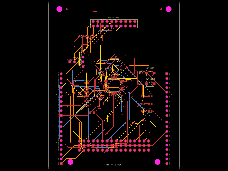 More from this authorShiboSoftwareDev/captivate-fr2676This circuit implements an MSP430FR2676 microcontroller-based development module with integrated power regulation, user interface components, programming interfaces, and sensor/boosterpack headers for embedded system prototyping.
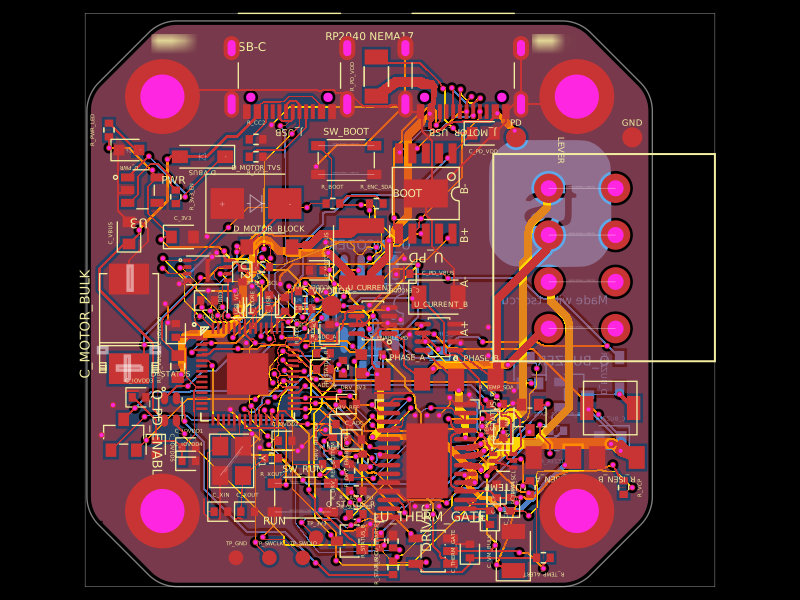 Similar packageastra/nema17-stepper-motor-controller-spring-clamp-rp2040A 4-layer RP2040 controller board that negotiates USB‑C PD motor power and drives a NEMA17 stepper via a DRV8825, with current sensing, thermal shutdown, RGB status LED, buzzer alarm, optional AS5600 encoder, protection/filtering, and test points.
 Discover something newpixalynx/esp32-usb-duckyA compact ESP32‑S3 USB‑C stick with native USB HID, 4‑bit microSD storage, 3.3V LDO power regulation, ESD protection, boot/reset controls, addressable RGB status LED, decoupling, and test pads.