shibosoftwaredev/f1c100s-linux-nema17-stepper-controller
Compact four-layer NEMA 17 carrier PCB combining an F1C100S Linux SoC, USB-C PD power and buck regulation, W5500 10/100 Ethernet, STM32 safety/motion control, and DRV8825 stepper-driver hardware with protection, sensing, connectors, and dual-sided SMT assembly.
- Version
- 0.4.15
- License
- unset
- Stars
- 0
ethernet.tsx
import { Fragment } from "react"
import { W5500 } from "./imports/W5500"
import { HR911105A } from "./imports/HR911105A"
import { X322525MSB4SI } from "./imports/X322525MSB4SI"

const wire = (name: string, from: string, to: string, thickness = 0.15) =>
  <trace name={name} from={from} to={to} thickness={thickness} />

const ethernetSchRotation: Record<string, number> = {
  R_ETH_RAIL_BC: 90,
  R_ETH_EXRES: -90,
}

const resistor = (name: string, value: string, lcsc: string, x: number, y: number, rotation = 0, schX = x, schY = y) =>
  <resistor name={name} layer="bottom" resistance={value} footprint="0402"
    supplierPartNumbers={{jlcpcb:[lcsc]}} pcbX={x} pcbY={y} pcbRotation={rotation}
    schX={schX} schY={schY} schRotation={ethernetSchRotation[name]} />

const bypass = (name: string, x: number, y: number, schX: number, schY: number, rotation = 0) => <>
  <capacitor name={name} layer="bottom" capacitance="100nF" maxVoltageRating={16} footprint="0402"
    maxDecouplingTraceLength={30}
    supplierPartNumbers={{jlcpcb:["C1525"]}} pcbX={x} pcbY={y} pcbRotation={rotation}
    schX={schX} schY={schY} schRotation={-90} />
  {wire(`${name}_GND`, `.${name} > .pin2`, "net.BOARD_GND")}
</>

/** W5500 gives the Linux system a deterministic 10/100 Ethernet interface over SPI1. */
export function EthernetSection() {
  const groundPins = [3,9,14,16,19,29,48]
  return <group name="ETHERNET" pcbX={0} pcbY={0} schX={27} schY={22} schSheetName="ethernet">
    <HR911105A name="J_ETH" layer="top" allowOffBoard pcbX={-13.15} pcbY={-11.9} pcbRotation={270}
      schX={-39} schY={-25}
      noConnect={["NC","pin8","pin9","pin10","pin11","pin12"]} />
    <W5500 name="U_ETH" layer="bottom" pcbX={5.5768} pcbY={-12.6605} pcbRotation={0}
      schX={-27} schY={-25} schWidth={2.435} schHeight={5}
      noConnect={["DNC","VBG","SPDLED","LINKLED","DUPLED","ACTLED","RSVD2","RSVD3","RSVD4","RSVD5","RSVD6"]} />

    {/* A ferrite bead isolates PHY switching current from the SoC rail. */}
    <chip name="FB_ETH" layer="bottom" manufacturerPartNumber="BLM18AG601SN1D"
      supplierPartNumbers={{jlcpcb:["C19330"]}} footprint="0603"
      pinLabels={{pin1:"V3V3",pin2:"ETH_3V3"}} pcbX={8.6} pcbY={-18.6} schX={-42} schY={-13} />
    {wire("ETH_BEAD_OUT", ".FB_ETH > .pin2", ".C_ETH_BULK > .pin1", 0.3)}
    <capacitor name="C_ETH_BULK" layer="bottom" capacitance="4.7uF" maxVoltageRating={25} footprint="0805"
      maxDecouplingTraceLength={12}
      manufacturerPartNumber="CL21A475KAQNNNE" supplierPartNumbers={{jlcpcb:["C1779"]}}
      pcbX={11.9} pcbY={-20.05} schX={-36} schY={-13} schRotation={-90} />
    {wire("ETH_BULK_GND", ".C_ETH_BULK > .pin2", "net.BOARD_GND", 0.3)}
    {wire("ETH_BULK_VDD", ".C_ETH_BULK > .pin1", ".R_ETH_RAIL_AB > .pin1", 0.3)}

    {/* Two fitted 0 ohm links keep the DC rail common while dividing its PCB
        topology into three small, deterministic routing zones. */}
    {resistor("R_ETH_RAIL_AB", "0", "C17168", 14.7, -20.05, 0, -38, -16)}
    {resistor("R_ETH_RAIL_BC", "0", "C17168", 16.8, -20.05, 0, -34, -16)}
    {resistor("R_ETH_A_CORE", "0", "C17168", 16.2, -10.3, 0, -42, -18)}
    {resistor("R_ETH_A_TCT", "0", "C17168", 18.3, -10.3, 0, -38, -18)}
    {resistor("R_ETH_B_CORE", "0", "C17168", 19.4, -13.8, 0, -30.08, -16)}
    {resistor("R_ETH_B_CTRL", "0", "C17168", 19.4, -15.3, 0, -26.88, -16)}
    {resistor("R_ETH_B_TX", "0", "C17168", 19.4, -16.8, 0, -22.11, -16)}
    {/* Strap PMODE[2:0] high through individual 10 k resistors.  Keeping the
        configuration pins behind resistors avoids a large direct copper tree
        on the W5500 analog rail and gives each mode input a clean local route. */}
    {resistor("R_ETH_PMODE2", "10k", "C25744", 11.5, -13.0, 90, -14, -18)}
    {resistor("R_ETH_PMODE1", "10k", "C25744", 11.5, -15.0, 90, -11.26, -19.5)}
    {resistor("R_ETH_PMODE0", "10k", "C25744", 11.5, -17.0, 90, -6, -18)}
    {/* These are explicit pad-to-pad trees rather than abstract multi-terminal
        nets.  Electrically they are the same three DC rail zones, but the
        explicit topology prevents the phased autorouter from inventing an
        ambiguous minimum-spanning-tree branch between phases. */}
    {wire("ETH_RAIL_A_CORE_IN", ".R_ETH_RAIL_AB > .pin1", ".R_ETH_A_CORE > .pin1", 0.25)}
    {wire("ETH_RAIL_AB_A", ".R_ETH_A_CORE > .pin2", ".U_ETH > .pin11", 0.25)}
    {wire("ETH_RAIL_A_TCT_IN", ".R_ETH_RAIL_AB > .pin1", ".R_ETH_A_TCT > .pin1", 0.25)}
    {wire("ETH_RAIL_AB_B", ".R_ETH_RAIL_AB > .pin2", ".R_ETH_B_CORE > .pin1", 0.25)}
    {wire("ETH_RAIL_B_CORE_OUT", ".R_ETH_B_CORE > .pin2", ".U_ETH > .pin15", 0.25)}
    {wire("ETH_RAIL_B_CTRL_IN", ".R_ETH_RAIL_AB > .pin2", ".R_ETH_B_CTRL > .pin1", 0.2)}
    {wire("ETH_RAIL_B_TX_IN", ".R_ETH_RAIL_AB > .pin2", ".R_ETH_B_TX > .pin1", 0.2)}
    {wire("ETH_RAIL_BC_B", ".R_ETH_RAIL_AB > .pin2", ".R_ETH_RAIL_BC > .pin1", 0.25)}
    {wire("ETH_RAIL_BC_C", ".R_ETH_RAIL_BC > .pin2", ".C_ETH_6 > .pin1", 0.25)}

    {/* The W5500 is a 0.5 mm-pitch QFN; 0.15 mm escapes preserve clearance
        between alternating AVDD/AGND pins before widening into the planes. */}
    {groundPins.map(pin => <Fragment key={pin}>
      {wire(`ETH_GROUND_${pin}`, `.U_ETH > .pin${pin}`, "net.BOARD_GND", 0.15)}
    </Fragment>)}
    {/* Each alternating AVDD/AGND pad has a dedicated local bypass. The AVDD
        rail itself is expressed as an acyclic component-to-component tree
        below so the router never has to synthesize a 24-endpoint MST. */}
    {bypass("C_ETH_1", 6.1, -18.5, -35, -32)}
    {bypass("C_ETH_2", 4.1, -18.5, -31, -32)}
    {bypass("C_ETH_3", 2.1, -18.5, -27, -32)}
    {bypass("C_ETH_4", -0.7, -15.55, -23, -32)}
    {bypass("C_ETH_5", -0.7, -14.3, -19, -32)}
    {bypass("C_ETH_6", -19, -29, -15, -32)}
    {bypass("C_ETH_7", -17, -29, -11, -32)}

    {/* Datasheet reference, regulator and oscillator support. */}
    {resistor("R_ETH_EXRES", "12.4k", "C11692", -25.5, -16, 0, -30, -13)}
    <trace name="ETH_EXRES" from=".U_ETH > .EXRES1" to=".R_ETH_EXRES > .pin1"
      thickness={0.15}
      pcbPath={[".U_ETH > .EXRES1", {x:1.75,y:-6}, ".R_ETH_EXRES > .pin1"]} />
    {wire("ETH_EXRES_GND", ".R_ETH_EXRES > .pin2", "net.BOARD_GND")}
    <capacitor name="C_ETH_TOCAP" layer="bottom" capacitance="4.7uF" maxVoltageRating={16} footprint="0603"
      manufacturerPartNumber="CL10A475KO8NNNC" supplierPartNumbers={{jlcpcb:["C19666"]}}
      pcbX={-1.3} pcbY={-12.1} pcbRotation={90} schX={-31} schY={-15} schRotation={-90} />
    {wire("ETH_TOCAP", ".U_ETH > .TOCAP", ".C_ETH_TOCAP > .pin1")}
    {wire("ETH_TOCAP_GND", ".C_ETH_TOCAP > .pin2", "net.BOARD_GND")}
    <capacitor name="C_ETH_1V2" layer="bottom" capacitance="10nF" maxVoltageRating={50} footprint="0402"
      maxDecouplingTraceLength={2}
      supplierPartNumbers={{jlcpcb:["C15195"]}} pcbX={0} pcbY={-10.65} pcbRotation={270}
      schX={-26} schY={-15} schRotation={-90} />
    <trace name="ETH_1V2" from=".U_ETH > .pin22" to=".C_ETH_1V2 > .pin1"
      thickness={0.12} maxLength={2} />
    <trace name="ETH_1V2_GND" from=".C_ETH_1V2 > .pin2" to="net.BOARD_GND"
      thickness={0.12} maxLength={2} />
    {wire("ETH_RSVD1_GND", ".U_ETH > .pin23", "net.BOARD_GND")}

    <X322525MSB4SI name="Y_ETH" layer="bottom" loadCapacitance="20pF" pcbX={12.8} pcbY={-9} pcbRotation={90}
      schX={-19.93} schY={-15} />
    <capacitor name="C_ETH_XI" layer="bottom" capacitance="22pF" maxVoltageRating={50} footprint="0402"
      manufacturerPartNumber="CL05C220JB5NNNC" supplierPartNumbers={{jlcpcb:["C70464"]}}
      pcbX={15.1} pcbY={-1.5} pcbRotation={90} schX={-24} schY={-15} schRotation={-90} />
    <capacitor name="C_ETH_XO" layer="bottom" capacitance="22pF" maxVoltageRating={50} footprint="0402"
      manufacturerPartNumber="CL05C220JB5NNNC" supplierPartNumbers={{jlcpcb:["C70464"]}}
      pcbX={16.2} pcbY={-7.5} pcbRotation={0} schX={-18} schY={-15} schRotation={-90} />
    <trace name="ETH_XI" from=".U_ETH > .pin30" to=".Y_ETH > .pin1"
      thickness={0.12} maxLength={15} maxViaCount={2}
      pcbPath={[".U_ETH > .pin30", {x:-0.249936,y:5.2605}, {x:6.8232,y:5.9605}, ".Y_ETH > .pin1"]} />
    <trace name="ETH_XO" from=".U_ETH > .XO" to=".Y_ETH > .pin3"
      thickness={0.12} maxLength={15} maxViaCount={2}
      pcbPath={[".U_ETH > .XO", {x:0.249936,y:5.2605}, {x:5.2232,y:5.6605}, ".Y_ETH > .pin3"]} />
    {wire("ETH_CRYSTAL_GND2", ".Y_ETH > .pin2", "net.BOARD_GND")}
    {wire("ETH_CRYSTAL_GND4", ".Y_ETH > .pin4", "net.BOARD_GND")}
    <trace name="ETH_XI_CAP" from=".Y_ETH > .pin1" to=".C_ETH_XI > .pin1"
      thickness={0.12} maxLength={15} maxViaCount={2}
      pcbPath={[".Y_ETH > .pin1", {x:1.1,y:-1.6}, {x:5,y:-1.6}, {x:6.11,y:-1.6}, ".C_ETH_XI > .pin1"]} />
    {wire("ETH_XI_CAP_GND", ".C_ETH_XI > .pin2", "net.BOARD_GND")}
    <trace name="ETH_XO_CAP" from=".Y_ETH > .pin3" to=".C_ETH_XO > .pin1"
      thickness={0.12} maxLength={15} maxViaCount={2} pcbStraightLine />
    {wire("ETH_XO_CAP_GND", ".C_ETH_XO > .pin2", "net.BOARD_GND")}

    {/* SPI1 and interrupt/reset lines are dedicated internal connections. */}
    {wire("ETH_CS", ".U_ETH > .SCSn", "net.ETH_CS")}
    {wire("ETH_MISO", ".U_ETH > .MISO", "net.ETH_MISO")}
    {wire("ETH_MOSI", ".U_ETH > .MOSI", "net.ETH_MOSI")}
    {wire("ETH_INT", ".U_ETH > .INTn", "net.ETH_INT")}
    {wire("ETH_RESET", ".U_ETH > .RSTn", "net.ETH_RST")}
    {resistor("R_ETH_RST", "10k", "C25744", -20, -14, 0, -13, -14)}
    {resistor("R_ETH_INT", "10k", "C25744", 17.5, -11.8, 0, -10, -14)}
    {wire("ETH_RST_PULLUP", ".R_ETH_RST > .pin1", "net.ETH_RST")}
    {wire("ETH_RST_PULLUP_VDD", ".R_ETH_RST > .pin2", ".R_ETH_B_CTRL > .pin2")}
    {wire("ETH_INT_PULLUP", ".R_ETH_INT > .pin1", "net.ETH_INT")}
    {wire("ETH_INT_PULLUP_VDD", ".R_ETH_INT > .pin2", ".R_ETH_B_CTRL > .pin2")}
    {wire("ETH_PMODE2_SIGNAL", ".U_ETH > .pin43", ".R_ETH_PMODE2 > .pin1")}
    {wire("ETH_PMODE2_PULLUP", ".R_ETH_PMODE2 > .pin2", ".C_ETH_1 > .pin1")}
    {wire("ETH_PMODE1_SIGNAL", ".U_ETH > .pin44", ".R_ETH_PMODE1 > .pin1")}
    {wire("ETH_PMODE1_PULLUP", ".R_ETH_PMODE1 > .pin2", ".C_ETH_1 > .pin1")}
    {wire("ETH_PMODE0_SIGNAL", ".U_ETH > .pin45", ".R_ETH_PMODE0 > .pin1")}
    {wire("ETH_PMODE0_PULLUP", ".R_ETH_PMODE0 > .pin2", ".C_ETH_1 > .pin1")}

    {/* Each small rail zone feeds only adjacent W5500 pads and bypasses. */}
    {wire("ETH_RAIL_A_8", ".U_ETH > .pin8", ".U_ETH > .pin11", 0.15)}
    {wire("ETH_RAIL_A_4", ".U_ETH > .pin4", ".U_ETH > .pin8", 0.15)}
    {wire("ETH_RAIL_A_C1", ".C_ETH_1 > .pin1", ".U_ETH > .pin4", 0.15)}
    {wire("ETH_RAIL_A_C2", ".C_ETH_2 > .pin1", ".U_ETH > .pin8", 0.15)}
    {wire("ETH_RAIL_A_C3", ".C_ETH_3 > .pin1", ".U_ETH > .pin11", 0.15)}
    {wire("ETH_RAIL_B_17", ".U_ETH > .pin17", ".U_ETH > .pin15", 0.15)}
    {wire("ETH_RAIL_B_C4", ".C_ETH_4 > .pin1", ".U_ETH > .pin15", 0.15)}
    {wire("ETH_RAIL_B_C5", ".C_ETH_5 > .pin1", ".U_ETH > .pin17", 0.15)}
    {wire("ETH_RAIL_C_28", ".U_ETH > .pin28", ".U_ETH > .pin21", 0.15)}
    {wire("ETH_RAIL_C_C6", ".C_ETH_6 > .pin1", ".U_ETH > .pin21", 0.15)}
    {wire("ETH_RAIL_C_C7", ".C_ETH_7 > .pin1", ".U_ETH > .pin28", 0.15)}

    {/* WIZnet MDI termination. TX is direct-coupled and each transmitter pin is
        biased to the analog rail through 49.9 ohm. RX is AC-coupled and each
        receiver pin is terminated to the receive center-tap bias node. */}
    {[
      ["TXN",2,-2.8,-14.8,0,-17,-20], ["TXP",1,-3.2,-17,0,-17,-22], ["RXN",6,-1,-17,0,-17,-24], ["RXP",3,-2.2,-18.0,0,-17,-26],
    ].map(([name,pin,x,y,rotation,schX,schY]) => <Fragment key={name as string}><group pcbX={0} pcbY={0} schX={0} schY={0}>
      {resistor(`R_ETH_${name}`, "49.9", "C25792", x as number, y as number, rotation as number, schX as number, schY as number)}
      {name === "TXN" || name === "TXP"
        ? name === "TXN"
          ? <trace name="ETH_TXN_CHIP" from=".U_ETH > .TXN" to=".J_ETH > .pin2" thickness={0.2}
              pcbPath={[
                ".U_ETH > .TXN",
                {x:2.9232,y:-5.0395,via:true,fromLayer:"bottom",toLayer:"inner2"},
                {x:-10.3768,y:-3.3395},
                {x:-10.3768,y:-3.3395,via:true,fromLayer:"inner2",toLayer:"bottom"},
                ".J_ETH > .pin2",
              ]} />
          : <trace name="ETH_TXP_CHIP" from=".U_ETH > .TXP" to=".J_ETH > .pin1" thickness={0.2}
              pcbPath={[
                ".U_ETH > .TXP",
                {x:2.2232,y:-5.5395,via:true,fromLayer:"bottom",toLayer:"inner1"},
                {x:-10.8768,y:-4.7395},
                {x:-10.8768,y:-4.7395,via:true,fromLayer:"inner1",toLayer:"bottom"},
                ".J_ETH > .pin1",
              ]} />
        : wire(`ETH_${name}_CHIP`, `.U_ETH > .${name}`, `.C_ETH_${name}_AC > .pin1`, 0.2)}
      {name === "TXN" || name === "TXP"
        ? <trace name={`ETH_${name}_JACK`} from={`.J_ETH > .pin${pin}`} to={`.R_ETH_${name} > .pin1`}
            thickness={0.2} pcbStraightLine />
        : wire(`ETH_${name}_JACK`, `.C_ETH_${name}_AC > .pin2`, `.J_ETH > .pin${pin}`, 0.2)}
    </group></Fragment>)}
    {wire("ETH_TCT", ".J_ETH > .pin4", ".R_ETH_TCT > .pin1", 0.3)}
    {wire("ETH_RCT", ".J_ETH > .pin5", "net.ETH_RX_BIAS", 0.3)}
    {wire("ETH_SHIELD1", ".J_ETH > .SH1", "net.BOARD_GND", 0.3)}
    {wire("ETH_SHIELD2", ".J_ETH > .SH2", "net.BOARD_GND", 0.3)}

    <silkscreentext text="ETHERNET 10/100" pcbX={-5.5} pcbY={-14.2} fontSize={0.75} />
  </group>
}
Related Packages
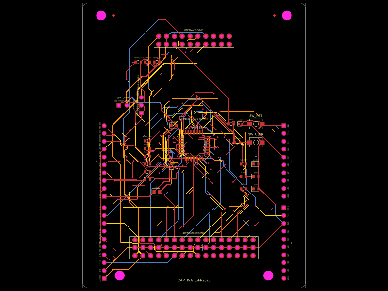 More from this authorShiboSoftwareDev/captivate-fr2676This circuit implements an MSP430FR2676 microcontroller-based development module with integrated power regulation, user interface components, programming interfaces, and sensor/boosterpack headers for embedded system prototyping.
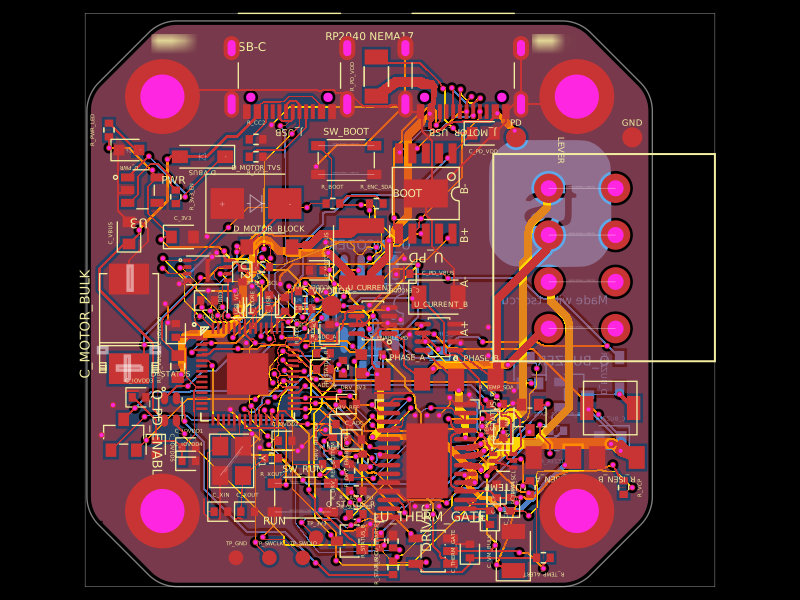 Similar packageastra/nema17-stepper-motor-controller-spring-clamp-rp2040A 4-layer RP2040 controller board that negotiates USB‑C PD motor power and drives a NEMA17 stepper via a DRV8825, with current sensing, thermal shutdown, RGB status LED, buzzer alarm, optional AS5600 encoder, protection/filtering, and test points.
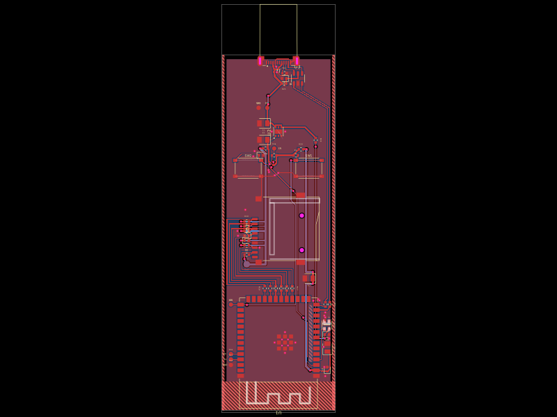 Discover something newpixalynx/esp32-usb-duckyA compact ESP32‑S3 USB‑C stick with native USB HID, 4‑bit microSD storage, 3.3V LDO power regulation, ESD protection, boot/reset controls, addressable RGB status LED, decoupling, and test pads.