shibosoftwaredev/f1c100s-linux-nema17-stepper-controller
Compact four-layer NEMA 17 carrier PCB combining an F1C100S Linux SoC, USB-C PD power and buck regulation, W5500 10/100 Ethernet, STM32 safety/motion control, and DRV8825 stepper-driver hardware with protection, sensing, connectors, and dual-sided SMT assembly.
- Version
- 0.4.15
- License
- unset
- Stars
- 0
electrical-corrections.tsx
import { footprints } from "./footprints"

const wire = (name: string, from: string, to: string, thickness = 0.15) =>
  <trace name={name} from={from} to={to} thickness={thickness} />

const r0402 = (name: string, value: string, lcsc: string, x: number, y: number, schX = x, schY = y, schSheetName?: string) =>
  <resistor name={name} layer="top" resistance={value} footprint="0402"
    supplierPartNumbers={{jlcpcb:[lcsc]}} pcbX={x} pcbY={y}
    schX={schX} schY={schY} schSheetName={schSheetName} />

const c0402 = (name: string, value: string, lcsc: string, x: number, y: number, schX = x, schY = y, schSheetName?: string, layer: "top" | "bottom" = "top", rotation = 0) =>
  <capacitor name={name} layer={layer} capacitance={value} maxVoltageRating={50} footprint="0402"
    supplierPartNumbers={{jlcpcb:[lcsc]}} pcbX={x} pcbY={y}
    pcbRotation={rotation} schX={schX} schY={schY} schRotation={-90} schSheetName={schSheetName} />

/**
 * Corrections deliberately render after the frozen carrier. This keeps all
 * established source/PCB identifiers stable while adding the protection and
 * Ethernet networks found during the electrical sign-off review.
 */
export function ElectricalCorrections() {
  return <group name="ELECTRICAL_CORRECTIONS" pcbX={0} pcbY={0} schX={0} schY={0}>
    {/* HUSB238A-controlled 30 V high-side switch. AO4407A pins 1-3 are Source,
        pin 4 Gate and pins 5-8 Drain. The internal leadframe connections are
        declared so all package pins participate in the high-current net. */}
    <chip name="Q_VBUS" layer="top" manufacturerPartNumber="AO4407A"
      supplierPartNumbers={{jlcpcb:["C3011194"]}} footprint={footprints.so8}
      pinLabels={{pin1:"S",pin2:"S2",pin3:"S3",pin4:"G",pin5:"D",pin6:"D2",pin7:"D3",pin8:"D4"}}
      internallyConnectedPins={[["pin1","pin2","pin3"],["pin5","pin6","pin7","pin8"]]}
      pcbX={18.3} pcbY={8.8} pcbRotation={270} schX={10} schY={9} schSheetName="pd_power" />
    {wire("VBUS_SWITCH_GATE", ".Q_VBUS > .pin4", ".R_PD_GOOD_PU > .pin1")}
    {wire("VBUS_SOURCE_1", ".Q_VBUS > .pin1", ".Q_VBUS > .pin2", 0.8)}
    {wire("VBUS_SOURCE_2", ".Q_VBUS > .pin2", ".Q_VBUS > .pin3", 0.8)}
    {wire("VBUS_SOURCE_3", ".Q_VBUS > .pin3", ".R_PD_GOOD_PU > .pin2", 0.25)}
    {wire("VBUS_DRAIN_5", ".Q_VBUS > .pin5", ".Q_VBUS > .pin6", 0.8)}
    {wire("VBUS_DRAIN_6", ".Q_VBUS > .pin6", ".Q_VBUS > .pin7", 0.8)}
    {wire("VBUS_DRAIN_7", ".Q_VBUS > .pin7", ".Q_VBUS > .pin8", 0.8)}
    {wire("BUCK_INPUT_BYPASS", ".C_BUCK_IN > .pin1", ".U_BUCK > .VIN", 0.8)}
    {/* W5500 / integrated-magnetics termination from the official WIZnet
        reference: 49.9 ohm TX pullups, AC-coupled RX and filtered center taps. */}
    <net name="ETH_RX_BIAS" nominalTraceWidth={0.2} />
    {c0402("C_ETH_RXN_AC", "6.8nF", "C1590", -0.12, -18.58, 16.85, -5, "ethernet", "bottom")}
    {c0402("C_ETH_RXP_AC", "6.8nF", "C1590", -3.37, -19.83, 17.15, -2, "ethernet", "bottom")}
    {r0402("R_ETH_TCT", "10", "C25077", -17, -15, 17, 1, "ethernet")}
    {c0402("C_ETH_TCT", "22nF", "C1532", -17, -17, 17.9, 4, "ethernet", "top", 180)}
    {/* Keep the RX center-tap bypass on the Ethernet (bottom) side.  On the
        top side this capacitor sat directly in the DRV8825 phase-output
        escape corridor to the NEMA17 connector. */}
    {c0402("C_ETH_RCT", "10nF", "C15195", -10, -14, 17.37, 7, "ethernet", "bottom")}

    {/* Express shared rails as nets rather than forcing several branches out
        of the same 0.5 mm-pitch QFN pad. This is electrically identical to
        the WIZnet reference and gives each termination its own via escape. */}
    {wire("ETH_TXN_TERM", ".R_ETH_TXN > .pin2", ".R_ETH_B_TX > .pin2")}
    {wire("ETH_TXP_TERM", ".R_ETH_TXP > .pin2", ".R_ETH_B_TX > .pin2")}
    <trace name="ETH_RXN_TERM_IN" from=".C_ETH_RXN_AC > .pin1" to=".R_ETH_RXN > .pin1"
      thickness={0.2} pcbStraightLine />
    {wire("ETH_RXN_TERM_BIAS", ".R_ETH_RXN > .pin2", "net.ETH_RX_BIAS", 0.2)}
    <trace name="ETH_RXP_TERM_IN" from=".C_ETH_RXP_AC > .pin1" to=".R_ETH_RXP > .pin1"
      thickness={0.2} pcbStraightLine />
    {wire("ETH_RXP_TERM_BIAS", ".R_ETH_RXP > .pin2", "net.ETH_RX_BIAS", 0.2)}
    {wire("ETH_TCT_FEED", ".R_ETH_A_TCT > .pin2", ".R_ETH_TCT > .pin2", 0.3)}
    {wire("ETH_TCT_DECOUPLE", ".C_ETH_TCT > .pin1", ".R_ETH_TCT > .pin1", 0.2)}
    {wire("ETH_TCT_DECOUPLE_GND", ".C_ETH_TCT > .pin2", "net.BOARD_GND", 0.2)}
    {wire("ETH_RCT_DECOUPLE", ".C_ETH_RCT > .pin1", "net.ETH_RX_BIAS", 0.2)}
    {wire("ETH_RCT_DECOUPLE_GND", ".C_ETH_RCT > .pin2", "net.BOARD_GND", 0.2)}
  </group>
}
Related Packages
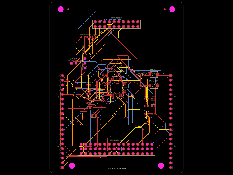 More from this authorShiboSoftwareDev/captivate-fr2676This circuit implements an MSP430FR2676 microcontroller-based development module with integrated power regulation, user interface components, programming interfaces, and sensor/boosterpack headers for embedded system prototyping.
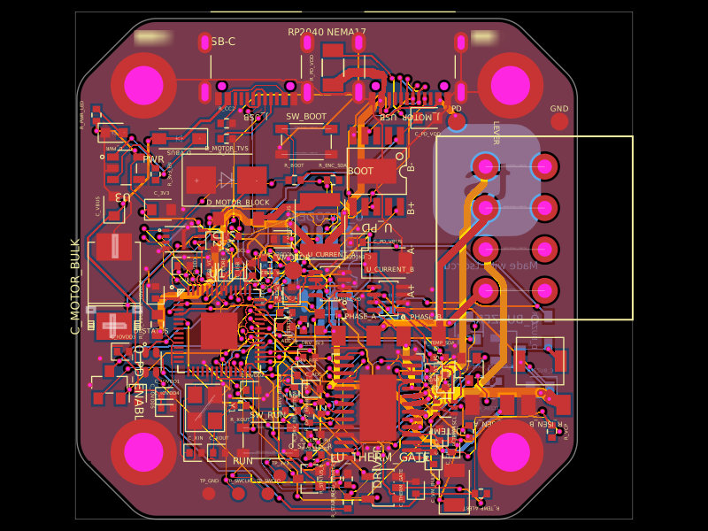 Similar packageastra/nema17-stepper-motor-controller-spring-clamp-rp2040A 4-layer RP2040 controller board that negotiates USB‑C PD motor power and drives a NEMA17 stepper via a DRV8825, with current sensing, thermal shutdown, RGB status LED, buzzer alarm, optional AS5600 encoder, protection/filtering, and test points.
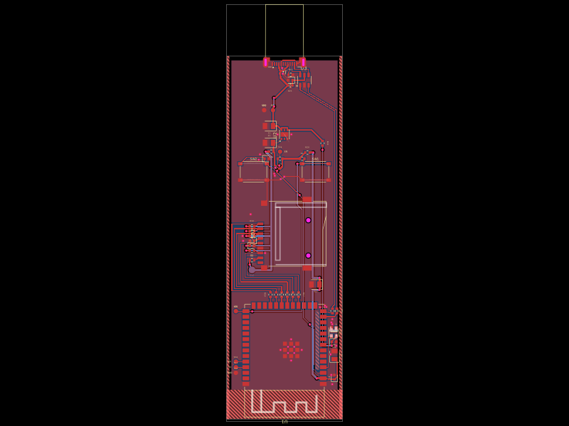 Discover something newpixalynx/esp32-usb-duckyA compact ESP32‑S3 USB‑C stick with native USB HID, 4‑bit microSD storage, 3.3V LDO power regulation, ESD protection, boot/reset controls, addressable RGB status LED, decoupling, and test pads.