shibosoftwaredev/f1c100s-linux-nema17-stepper-controller
Compact four-layer NEMA 17 carrier PCB combining an F1C100S Linux SoC, USB-C PD power and buck regulation, W5500 10/100 Ethernet, STM32 safety/motion control, and DRV8825 stepper-driver hardware with protection, sensing, connectors, and dual-sided SMT assembly.
- Version
- 0.4.15
- License
- unset
- Stars
- 0
compact-layout.ts
import { repositionPcbComponentTo } from "@tscircuit/circuit-json-util"
type Point = { x: number; y: number }
type Rect = Point & { w: number; h: number; id: string }
type PcbLayer = "top" | "inner1" | "inner2" | "bottom"
const BOARD_LAYER_STACK: PcbLayer[] = ["top", "inner1", "inner2", "bottom"]
const viaLayersBetween = (from: PcbLayer, to: PcbLayer) => {
const fromIndex = BOARD_LAYER_STACK.indexOf(from)
const toIndex = BOARD_LAYER_STACK.indexOf(to)
const layers = BOARD_LAYER_STACK.slice(Math.min(fromIndex, toIndex), Math.max(fromIndex, toIndex) + 1)
return fromIndex <= toIndex ? layers : layers.reverse()
}
const BOARD_HALF = 21.15
const EDGE_CLEARANCE = 0.35
// Courtyards already include package clearance; retain an additional 0.08 mm
// placement margin while allowing sub-2 mm bypass connections at fine-pitch ICs.
const PART_GAP = 0.08
const fixedPlacements: Record<string, Point & { rotation?: number; allowOffBoard?: boolean }> = {
// Keep both Type-C shells inside the 42.3 mm outline. Their cable-entry
// faces are flush with the north edge instead of hanging over the motor.
J_USB_DATA: { x: -6, y: 17.25, rotation: 180 },
// The rendered Type-C origin is offset 0.425 mm from its courtyard center.
// These coordinates leave both complete shells inside the 42.3 mm outline.
J_USB_PWR: { x: 16.0, y: 17.25, rotation: 180 },
// Fabricated normally-closed boot link. Its 1.7 x 0.8 mm copper envelope is
// clear of both the upper-left mounting annulus and the DATA USB-C shell.
JP_BOOT: { x: -13.3, y: 19.45, rotation: 0 },
// Recess the jack 1.25 mm from the proven route position so both shield
// annuli clear the strict left edge by at least 0.25 mm. The housing may
// overhang for cable access; no drilled or copper feature does.
J_ETH: { x: -13.15, y: -11.9, rotation: 270, allowOffBoard: true },
// Preserve the proven reset-switch pocket instead of allowing the final
// packer pass to consume it after the motion bypass is fixed in place.
SW_RESET: { x: -13.3, y: 10.55, rotation: 0 },
// The phase connector occupies the clear lower-left channel, away from the
// (+15.5,-15.5) NEMA 17 tie screw. Its physical left-to-right pin order is
// A+, A-, B-, B+ (logical pins 4, 3, 2, 1).
// Recess the phase connector 0.5 mm so all four plated pins and annuli are
// inside the strict 42.3 mm square while the cable-entry body may overhang.
J_MOTOR: { x: 3, y: -19.5, rotation: 0, allowOffBoard: true },
// Fix the thermal-via footprint before PCB primitives are emitted. Moving
// the package after footprint render would leave its exposed-pad via array
// behind instead of translating it with the driver.
// Keep the driver and its escape vias entirely west of the bottom-side
// W5500 pad field. Their former coincident placement made any through-via
// fanout physically collide with the IC on the opposite assembly face.
U_MOTOR: { x: 1.2, y: -11.5, rotation: 0 },
// Place the DRV8825 flying capacitor directly below CP1/CP2. This keeps the
// high-dV/dt loop short and avoids crossing the temperature-supply trunk.
C_CP: { x: -3.2, y: -16.1, rotation: 0 },
C_VCP: { x: -3.22, y: -17.33, rotation: 0 },
// Align each VM bypass capacitor's positive pad directly below its matching
// DRV8825 supply pin. This removes the former neck-down between neighbouring
// passives and permits a full-width motor-supply entry on the fixed outline.
C_VMA: { x: -1.3, y: -16.1, rotation: 0 },
C_VMB: { x: 3.985, y: -16.1, rotation: 0 },
F_VM: { x: 10.4, y: -8.85, rotation: 0 },
D_VM_BLOCK: { x: 9.3, y: -3.0, rotation: 180 },
D_VM_TVS: { x: 17.1, y: -9.3, rotation: 180 },
C_VM_BULK: { x: 18.236, y: -0.775625, rotation: 90 },
C_VM_CER: { x: 15.98, y: -19.67, rotation: 180 },
Q_PD_ENABLE: { x: 10.7, y: -13.1388, rotation: 90 },
R_ENABLE_PD: { x: 10.7, y: -16.4, rotation: 0 },
R_REF_TOP: { x: 8, y: -14.8, rotation: 0 },
R_REF_BOTTOM: { x: 8, y: -16.5, rotation: 0 },
C_REF: { x: 6, y: -16.5, rotation: 0 },
// Keep the TPS54302 and its feedback star at the same coordinates at source
// render and final placement so the deterministic FB copper remains local.
U_BUCK: { x: -13.022, y: 4.8288, rotation: 90 },
L_BUCK: { x: -13.9418, y: 0.043, rotation: 90 },
R_BUCK_TOP: { x: -16.87, y: 6.17, rotation: 0 },
C_BUCK_FF: { x: -18.87, y: 6.17, rotation: 0 },
R_BUCK_FF: { x: -19.37, y: 7.42, rotation: 0 },
R_BUCK_BOTTOM: { x: -19.37, y: 8.67, rotation: 0 },
// HF input bypass sits directly above the VIN pad; keep this fixed so the
// generic packer cannot trade away the controller's 1 mm decoupling limit.
C_BUCK_IN_HF: { x: -9.8, y: 5.73, rotation: 0 },
C_BUCK_OUT2: { x: -18.1, y: 0.0, rotation: 0 },
// Put the safety MCU directly behind the Linux module. This clear backside
// pocket avoids the top-mounted magjack's through-hole pin field.
U_MOTION: { x: -1.75, y: 2.0, rotation: 180 },
C_MOTION: { x: -2.4, y: 7.1, rotation: 270 },
// Face the source pins toward the USB-C receptacle. Raw VBUS then enters
// the high-side switch directly; protected VBUS faces the buck converter.
Q_VBUS: { x: 18.3, y: 8.8, rotation: 270 },
// Leave the PD bypass in its previously placement-clean pocket. Moving it
// next to VDD put its courtyard through the HUSB238 body.
C_PD_VDD: { x: 14.3, y: 15.2, rotation: 270 },
// Lock the asymmetric QFN footprint's rendered center so moving its bypass
// capacitor cannot shift every CC/GATE escape by a packing-grid step.
U_PD: { x: 17.3, y: 15.228, rotation: 90 },
R_PD_GOOD_PU: { x: 18.2, y: 18, rotation: 180 },
R_V3V3_RIGHT: { x: 14.2, y: 13.2, rotation: 0 },
R_V3V3_ETH: { x: 15.0, y: 4.5, rotation: 0 },
// Put the W5500 series clock resistor in the open corridor to the right of
// the PE breakouts. This avoids crossing the SoC supply-reference fanout
// and leaves short, independent approaches for both clock-net segments.
R_ETH_SCLK: { x: 7.0, y: -5.5, rotation: 0 },
R_ETH_INT: { x: 17.5, y: -11.8, rotation: 0 },
// Compact USB2 protector immediately below the data receptacle. This clear
// pocket is outside the SoC fanout and keeps the ESD path short.
U_USB_ESD: { x: -9.4, y: 11.3, rotation: 0 },
C_ESD: { x: -9.5, y: 8.8, rotation: 0 },
R_V3V3_MOTOR: { x: -3.37, y: -6.08, rotation: 0 },
// Keep the driver fault bias and temperature support inside the motor
// domain instead of allowing the generic packer to scatter them to the
// opposite board edges.
R_FAULT_PU: { x: -2.5, y: -6.8, rotation: 0 },
U_TEMP: { x: 12.0, y: -19.0, rotation: 0 },
C_TEMP: { x: 9.5, y: -20.3, rotation: 0 },
R_TEMP_ALERT: { x: 9.2, y: -18.0, rotation: 0 },
// RX coupling/termination pairs share the clear strip below the W5500.
// Keeping each resistor beside its capacitor prevents a long bias stub.
C_ETH_RXN_AC: { x: -0.12, y: -18.58, rotation: 0 },
R_ETH_RXN: { x: -1, y: -17, rotation: 0 },
C_ETH_RXP_AC: { x: -3.37, y: -19.83, rotation: 0 },
// Clear the shifted through-hole motor connector and adjacent RX passives;
// the bottom-side resistor still remains within 3 mm of its coupling cap.
R_ETH_RXP: { x: -2.2, y: -18.0, rotation: 0 },
// With U_ETH oriented so its MDI pins face the magnetics, the 1.2 V
// decoupler belongs at the left-side pin 22/23 pair.
C_ETH_1V2: { x: 0, y: -10.65, rotation: 270 },
U_ETH: { x: 5.5768, y: -12.6605, rotation: 0 },
FB_ETH: { x: 8.6, y: -18.6, rotation: 0 },
C_ETH_BULK: { x: 11.9, y: -20.05, rotation: 0 },
Y_ETH: { x: 12.8, y: -9, rotation: 90 },
C_ETH_XI: { x: 15.1, y: -1.5, rotation: 90 },
C_ETH_XO: { x: 16.2, y: -7.5, rotation: 0 },
// Bottom-side RX center-tap bypass, kept out of both the W5500 rail trunk
// and the top-side DRV8825 phase-output escape corridor.
C_ETH_RCT: { x: -3.37, y: -10.3, rotation: 0 },
R_ETH_TXN: { x: -2.8, y: -14.8, rotation: 0 },
R_ETH_TXP: { x: -3.2, y: -17, rotation: 0 },
R_ETH_RAIL_AB: { x: 14.7, y: -20.05, rotation: 0 },
R_ETH_RAIL_BC: { x: 16.8, y: -20.05, rotation: 0 },
R_ETH_A_CORE: { x: 16.2, y: -10.3, rotation: 0 },
R_ETH_A_TCT: { x: 18.3, y: -10.3, rotation: 0 },
R_ETH_PMODE2: { x: 11.5, y: -13.0, rotation: 90 },
R_ETH_PMODE1: { x: 11.5, y: -15.0, rotation: 90 },
R_ETH_PMODE0: { x: 11.5, y: -17.0, rotation: 90 },
C_ETH_1: { x: 6.1, y: -18.5, rotation: 0 },
C_ETH_2: { x: 4.1, y: -18.5, rotation: 0 },
C_ETH_3: { x: 2.1, y: -18.5, rotation: 0 },
C_ETH_4: { x: -0.7, y: -15.55, rotation: 0 },
C_ETH_5: { x: -0.7, y: -14.3, rotation: 0 },
C_ETH_TOCAP: { x: -1.3, y: -12.1, rotation: 90 },
R_ETH_B_CORE: { x: 19.4, y: -13.8, rotation: 0 },
R_ETH_B_CTRL: { x: 19.4, y: -15.3, rotation: 0 },
R_ETH_B_TX: { x: 19.4, y: -16.8, rotation: 0 },
U_2V5: { x: 17.4, y: -4.25, rotation: 0 },
C_U_2V5_IN: { x: 20.2, y: -5.8, rotation: 90 },
C_U_2V5_OUT: { x: 20.2, y: -2.7, rotation: 90 },
U_1V2: { x: 17.4, y: 1.95, rotation: 0 },
C_U_1V2_IN: { x: 20.2, y: 0.4, rotation: 90 },
C_U_1V2_OUT: { x: 20.2, y: 3.5, rotation: 90 },
U_2V8: { x: 17.4, y: 8.15, rotation: 0 },
C_U_2V8_IN: { x: 20.2, y: 6.6, rotation: 90 },
C_U_2V8_OUT: { x: 20.2, y: 9.7, rotation: 90 },
// Face each HUSB238 programming resistor toward its corresponding QFN pin;
// none of these parts owns accepted carrier copper yet.
R_PD_VSET: { x: 13.9, y: 17.0, rotation: 0 },
R_PD_ISET: { x: 16.4, y: 12.55, rotation: 0 },
R_PD_DEBUG: { x: 17.93, y: 11.5, rotation: 90 },
// Keep the USB2 Rd parts on the motor-side edge pocket, directly behind the
// respective CC pads rather than routing both across the receptacle holes.
R_USB_DATA_CC1: { x: -1.5, y: 13.5, rotation: 180 },
R_USB_DATA_CC2: { x: -11, y: 13.5, rotation: 180 },
C_B_AVCC: { x: -2.5, y: 12.9, rotation: 180 },
C_B_VCC_DRAM: { x: -5.8, y: -2.9, rotation: 180 },
C_VRA2: { x: -3.4, y: 13.0, rotation: 90 },
R_VRA2: { x: -5.6, y: 13.0, rotation: 0 },
C_B_VCC_TV: { x: 9.8, y: 13.6, rotation: 0 },
C_TV_REF: { x: 9.2, y: 16.6, rotation: 0 },
R_PU_SPI0_CS: { x: -8.7, y: -1.0, rotation: 0 },
}
// Recessing the connector shells consumes the north-edge component area.
// These low-profile module passives retain their XY locations on the back.
const bottomSideNames = new Set([
"C_B_VCC_DRAM", "C_VRA2", "R_VRA2", "C_B_VCC_TV", "C_TV_REF", "R_PU_SPI0_CS",
// This low-current charge-pump bleed is the only motor-stage passive moved
// to the rear face. It opens legal top-layer AOUT1/AOUT2 channels without
// enlarging the NEMA17 outline.
"R_VCP",
])
const topSideNames = new Set([
"J_USB_DATA", "J_USB_PWR", "J_ETH", "J_MOTOR",
// User-facing controls and intentionally tall/high-energy parts face away
// from the motor. All remaining support electronics are motor-side SMT.
"SW_RESET", "JP_BOOT", "F_VM", "D_VM_BLOCK", "D_VM_TVS",
"C_VM_BULK", "C_VM_CER",
// Keep the complete high-current/thermal motor stage on the outward face.
"U_MOTOR", "U_TEMP", "C_CP", "C_DRV_3V3", "C_REF", "C_TEMP",
"C_VCP", "C_VMA", "C_VMB", "R_ENABLE_PD", "R_FAULT_PU",
"R_REF_BOTTOM", "R_REF_TOP",
"R_TEMP_ALERT",
"Q_VBUS",
"Q_PD_ENABLE",
"R_ETH_SCLK",
"R_V3V3_ETH",
"U_USB_ESD", "C_ESD",
"MH1", "MH2", "MH3", "MH4",
])
const setProp = (node: any, key: string, value: unknown) => {
if (node._parsedProps) node._parsedProps[key] = value
}
const deleteProp = (node: any, key: string) => {
if (node._parsedProps) node._parsedProps[key] = undefined
}
const hasAncestorNamed = (node: any, name: string) => {
for (let current = node; current; current = current.parent)
if (current.props?.name === name) return true
return false
}
const routingPhaseForTrace = (node: any) => {
if (hasAncestorNamed(node, "SOC")) return undefined
const traceName = node.props?.name as string | undefined
// Escape the bottom-edge W5500 clock/RX pads and reserve the four motor
// output channels before any lower-priority local support routing.
if (traceName === "ETH_SCLK_DIRECT") return 5
if (traceName?.startsWith("V3V3_ETH_")) return 6
if (traceName === "V3V3_MOTOR_LINK_OUT") return 6
if (["MOTOR_FAULT_PULLUP_3V3", "TEMP_VDD", "TEMP_ALERT_PULLUP_3V3"].includes(traceName ?? "")) return 7
if (["MOTOR_A_PLUS", "MOTOR_A_MINUS", "MOTOR_B_PLUS", "MOTOR_B_MINUS", "TRACE_MOTOR_FAULT"].includes(traceName ?? "")) return 2
if (traceName === "VM_FUSED") return 5
if (hasAncestorNamed(node, "MOTOR_STAGE")) {
// The two current-sense returns cross the driver's bottom-edge escape and
// must claim that corridor before the charge-pump and motor-output runs.
if (["DRV_ISEN_A", "DRV_ISEN_B"].includes(traceName ?? "")) return 2
// Solve the current-sense, motor-output and charge-pump escapes together.
// Pipeline 9 cannot reliably reload the dense DRV8825 escape as immutable
// copper in the immediately following phase, while a joint solve keeps
// the same geometry collision-aware from the outset.
if (["DRV_CP1", "DRV_CP2", "DRV_VCP", "DRV_VCP_PULL"].includes(traceName ?? "")) return 2
if (["DRV_C_VMA", "DRV_C_VMB"].includes(traceName ?? "")) return 4
if (["DRV_3V3_BYPASS", "DRV_REF_FEED"].includes(traceName ?? "")) return 6
if (["DRV_ENABLE_ACTIVE", "DRV_MODE0", "DRV_MODE1", "TEMP_ADDR", "TEMP_BYPASS"].includes(traceName ?? "")) return 7
return 6
}
// Route the tight AP2112 output-ground escape in the small local phase,
// before the remaining board-level support connections.
if (traceName === "U_2V8_LOCAL_GND" || traceName === "C_U_2V8_OUT_SUPPLY") return 13
if (traceName?.startsWith("C_U_") || traceName?.startsWith("U_2V")) return 13
// All MDI branches that share W5500 or magjack pins must be solved in one
// phase. Splitting the reference termination network into a later phase
// can strand the second branch behind the first branch's pin escape.
// Keep the W5500's dense local supply/oscillator fanout separate from its
// MDI pair and the cross-board SPI/control bus. A single 57-connection
// Ethernet phase exhausts Pipeline 9 even though each of these groups is
// independently routable on the four-layer stack.
if (/^ETH_(TX|RX|TCT|RCT)/.test(traceName ?? "")) return 9
if (["ETH_CS", "ETH_MOSI", "ETH_MISO", "ETH_RESET", "ETH_INT"].includes(traceName ?? "")) return 10
if (traceName?.startsWith("ETH_")) return 8
if (traceName?.startsWith("BUCK_")) return 3
if (traceName?.startsWith("VBUS_") || traceName === "PD_GOOD_REMOTE") return 1
if (traceName === "ESD_DM_BRIDGE" || traceName === "ESD_DP_BRIDGE" || traceName === "C_ESD_SUPPLY") return 1
// Leave the two short Type-C configuration-channel runs until the dense
// power and signal escapes are fixed. Routing them in the initial PD phase
// made the next phase unnecessarily re-solve a preloaded CC trace.
if (traceName === "PD_CC1" || traceName === "PD_CC2") return 12
if (hasAncestorNamed(node, "PD_POWER") || hasAncestorNamed(node, "USB_PORT_SPLIT")) return 1
if (hasAncestorNamed(node, "ETHERNET")) return 8
if (hasAncestorNamed(node, "MOTION")) {
if (traceName === "MOTION_UART_RX") return 14
if (traceName === "MOTION_UART_TX") return 15
if (["MOTION_BOOT", "MOTION_BOOT_PULLDOWN", "MOTION_TP_SWCLK"].includes(traceName ?? "")) return 16
if (["MOTION_NRST", "MOTION_RESET_PULLUP", "MOTION_RESET_CAP", "MOTION_TP_NRST"].includes(traceName ?? "")) return 17
if (traceName === "MOTION_STEP") return 18
if (traceName === "MOTION_DIR") return 19
if (["MOTION_ENABLE_RAW", "PD_GATE_SOURCE", "MOTION_ENABLE_RAW_PD"].includes(traceName ?? "")) return 20
if (["PD_GATE_DRAIN", "MOTOR_ENABLE_PD"].includes(traceName ?? "")) return 21
if (traceName === "MOTION_FAULT") return 22
if (traceName === "MOTION_TEMP_ALERT") return 23
if (traceName === "MOTION_I2C_SCL") return 24
if (traceName === "MOTION_I2C_SDA") return 25
return 11
}
// Board-level regulator, flash, USB-protection and correction traces.
return 26
}
// These are short, unobstructed component-to-bypass-capacitor connections.
// Keeping them direct avoids spending an entire autorouting phase re-solving
// geometry that is fixed by the DRV8825 placement itself.
// The compact placement is retained, but all JSX pcbPath hints are removed.
// Paths authored against earlier board sizes were the dominant source of
// final copper collisions and must not bypass the same DRC-aware autorouter
// used for the rest of the board.
const preservedManualTraceNames = new Set<string>()
/** Apply the two-sided assembly plan before footprints are emitted. */
export function applyCompactComponentPlan(board: any) {
const walk = (node: any) => {
const name = node.props?.name as string | undefined
if (node.componentName === "Trace") {
// Every old hand-authored path was tied to the former 81 x 70 mm PCB.
// Preserve electrical endpoints and constraints, but route from scratch.
if (!preservedManualTraceNames.has(name ?? "")) {
deleteProp(node, "pcbPath")
deleteProp(node, "pcbStraightLine")
deleteProp(node, "maxViaCount")
// The SoC breakout-via row blocks a same-layer escape from W5500
// pins 30/31. Keep the oscillator loop below 10 mm, but permit the
// two short layer changes needed to pass beneath that row.
if (["ETH_XI", "ETH_XO", "ETH_XI_CAP", "ETH_XO_CAP"].includes(name ?? ""))
setProp(node, "maxViaCount", 2)
}
// The final board uses one deterministic global fabrication route set.
// Do not split it back into the exploratory per-net routing phases.
}
if (node._parsedProps && node.pcb_component_id === undefined && name) {
const isSoc = hasAncestorNamed(node, "SOC")
setProp(node, "layer", bottomSideNames.has(name)
? "bottom"
: isSoc || topSideNames.has(name) ? "top" : "bottom")
const fixed = fixedPlacements[name]
if (fixed) {
setProp(node, "pcbX", fixed.x)
setProp(node, "pcbY", fixed.y)
if (fixed.rotation !== undefined) setProp(node, "pcbRotation", fixed.rotation)
if (fixed.allowOffBoard) setProp(node, "allowOffBoard", true)
}
}
for (const child of node.children ?? []) walk(child)
}
walk(board)
}
const overlaps = (a: Rect, b: Rect, gap = PART_GAP) =>
Math.abs(a.x - b.x) < (a.w + b.w) / 2 + gap &&
Math.abs(a.y - b.y) < (a.h + b.h) / 2 + gap
const insideBoard = (r: Rect) =>
r.x - r.w / 2 >= -BOARD_HALF + EDGE_CLEARANCE &&
r.x + r.w / 2 <= BOARD_HALF - EDGE_CLEARANCE &&
r.y - r.h / 2 >= -BOARD_HALF + EDGE_CLEARANCE &&
r.y + r.h / 2 <= BOARD_HALF - EDGE_CLEARANCE
const sourceGroupPath = (db: any, sourceComponent: any) => {
const names: string[] = []
let id = sourceComponent?.source_group_id
while (id) {
const group = db.source_group.get(id)
if (!group) break
names.push(group.name ?? "")
id = group.parent_source_group_id
}
return names.reverse()
}
const componentRect = (db: any, pcb: any, id: string, symmetricForMove = true): Rect => {
let minX = pcb.center.x - pcb.width / 2
let maxX = pcb.center.x + pcb.width / 2
let minY = pcb.center.y - pcb.height / 2
let maxY = pcb.center.y + pcb.height / 2
for (const courtyard of db.toArray().filter((element: any) =>
element.pcb_component_id === pcb.pcb_component_id &&
element.type.startsWith("pcb_courtyard_"))) {
if (courtyard.center && courtyard.width !== undefined && courtyard.height !== undefined) {
const rotation = ((courtyard.ccw_rotation ?? 0) % 360 + 360) % 360
const width = rotation === 90 || rotation === 270 ? courtyard.height : courtyard.width
const height = rotation === 90 || rotation === 270 ? courtyard.width : courtyard.height
minX = Math.min(minX, courtyard.center.x - width / 2)
maxX = Math.max(maxX, courtyard.center.x + width / 2)
minY = Math.min(minY, courtyard.center.y - height / 2)
maxY = Math.max(maxY, courtyard.center.y + height / 2)
}
for (const point of courtyard.outline ?? []) {
minX = Math.min(minX, point.x); maxX = Math.max(maxX, point.x)
minY = Math.min(minY, point.y); maxY = Math.max(maxY, point.y)
}
}
if (!symmetricForMove)
return { id, x: (minX + maxX) / 2, y: (minY + maxY) / 2, w: maxX - minX, h: maxY - minY }
// Keep a movable component's center as the placement anchor and
// conservatively make its collision box symmetric around it.
const halfW = Math.max(pcb.center.x - minX, maxX - pcb.center.x)
const halfH = Math.max(pcb.center.y - minY, maxY - pcb.center.y)
return { id, x: pcb.center.x, y: pcb.center.y, w: 2 * halfW, h: 2 * halfH }
}
const nearPlacement: Record<string, { anchor: string; dx: number; dy: number }> = {
C_CP: { anchor: "U_MOTOR", dx: -5.7, dy: -4.8 },
C_VCP: { anchor: "U_MOTOR", dx: -3.2, dy: -5.0 },
R_VCP: { anchor: "U_MOTOR", dx: -5.7, dy: -6.3 },
C_VMA: { anchor: "U_MOTOR", dx: -2.5, dy: -4.6 },
C_VMB: { anchor: "U_MOTOR", dx: 2.785, dy: -4.6 },
// Vertical 1206 sense resistors occupy the clear bank immediately left of
// the driver, below the input fuse; this keeps the Kelvin runs local while
// leaving the four motor-output channels unobstructed.
R_ISEN_A: { anchor: "U_MOTOR", dx: -7.2, dy: -2.2 },
R_ISEN_B: { anchor: "U_MOTOR", dx: -10.0, dy: -2.2 },
C_DRV_3V3: { anchor: "U_MOTOR", dx: 5.8, dy: 3.0 },
R_REF_TOP: { anchor: "U_MOTOR", dx: 10.7, dy: 5.2 },
R_REF_BOTTOM: { anchor: "R_REF_TOP", dx: 2.0, dy: 0 },
C_REF: { anchor: "R_REF_BOTTOM", dx: 0, dy: -1.25 },
// The 180° W5500 puts its oscillator pins at the lower edge. The 90° crystal
// fits in the narrow channel between the W5500 and the bottom-side magjack,
// keeping both oscillator connections below the 10 mm limit.
C_ETH_1V2: { anchor: "U_ETH", dx: 5.3, dy: -1.75 },
C_ETH_TOCAP: { anchor: "U_ETH", dx: 5.6, dy: 0.75 },
Y_ETH: { anchor: "U_ETH", dx: -7.3, dy: -2.4 },
C_ETH_XI: { anchor: "Y_ETH", dx: 0, dy: -4.2 },
C_ETH_XO: { anchor: "Y_ETH", dx: 0, dy: 4.2 },
R_ETH_EXRES: { anchor: "U_ETH", dx: 6.4, dy: 4.0 },
R_ETH_SCLK: { anchor: "U_ETH", dx: 4.2, dy: -6.0 },
R_ETH_RAIL_AB: { anchor: "U_ETH", dx: 8.0, dy: 4.5 },
R_ETH_RAIL_BC: { anchor: "U_ETH", dx: 8.0, dy: 2.8 },
// One bypass per W5500 AVDD/VDD pad, arranged around the QFN perimeter.
C_ETH_1: { anchor: "U_ETH", dx: -1.5, dy: 6.2 },
C_ETH_2: { anchor: "U_ETH", dx: 0.5, dy: 6.2 },
C_ETH_3: { anchor: "U_ETH", dx: 2.5, dy: 6.2 },
C_ETH_4: { anchor: "U_ETH", dx: 6.2, dy: 1.7 },
C_ETH_5: { anchor: "U_ETH", dx: 6.2, dy: 0.2 },
C_ETH_6: { anchor: "U_ETH", dx: 6.2, dy: -1.3 },
C_ETH_7: { anchor: "U_ETH", dx: 1.7, dy: -6.2 },
// The receive AC capacitors and terminations occupy the 6 mm bottom-side
// channel between the magjack body and the W5500.
C_ETH_RXN_AC: { anchor: "U_ETH", dx: -9.3, dy: 3.2 },
R_ETH_RXN: { anchor: "C_ETH_RXN_AC", dx: 0.5, dy: 1.25 },
C_ETH_RXP_AC: { anchor: "U_ETH", dx: -9.3, dy: 1.65 },
R_ETH_RXP: { anchor: "C_ETH_RXP_AC", dx: 2.0, dy: 1.25 },
// Local analog-supply bank in the unobstructed strip above/right of W5500.
C_ETH_BULK: { anchor: "U_ETH", dx: 11.5, dy: 6.0 },
FB_ETH: { anchor: "U_ETH", dx: 13.6, dy: 6.0 },
R_ETH_RST: { anchor: "U_ETH", dx: 10.5, dy: 2.8 },
R_ETH_INT: { anchor: "U_ETH", dx: 12.5, dy: 2.8 },
R_ETH_TXN: { anchor: "U_ETH", dx: 10.5, dy: 1.3 },
R_ETH_TXP: { anchor: "U_ETH", dx: 12.5, dy: 1.3 },
C_MOTION: { anchor: "U_MOTION", dx: -0.65, dy: -5 },
// Use the open left-edge pocket for the motion rail's bulk reservoir. This
// keeps its link to the 100 nF bypass below the 10 mm electrical limit.
C_MOTION_BULK: { anchor: "C_MOTION", dx: -5.4, dy: 8.5 },
R_MOTION_RESET: { anchor: "U_MOTION", dx: -4.5, dy: 3.0 },
TP_MOTION_SWDIO: { anchor: "U_MOTION", dx: -5.0, dy: -3.0 },
TP_MOTION_SWCLK: { anchor: "U_MOTION", dx: -5.0, dy: -1.0 },
TP_MOTION_NRST: { anchor: "U_MOTION", dx: -5.0, dy: 1.0 },
TP_MOTION_GND: { anchor: "U_MOTION", dx: -5.0, dy: 3.0 },
// Keep the PD controller's GPIO-programming resistors in its local bottom-
// side pocket. Letting the generic packer scatter them across the board
// creates unnecessarily long high-impedance configuration traces. The
// GATE pull-up remains beside the high-side switch at the opposite edge.
C_PD_VDD: { anchor: "U_PD", dx: 2.6, dy: 3.15 },
R_PD_VSET: { anchor: "U_PD", dx: -3.4, dy: 1.4 },
R_PD_ISET: { anchor: "U_PD", dx: -3.4, dy: 0.2 },
R_PD_DEBUG: { anchor: "U_PD", dx: -3.4, dy: -1.0 },
R_PD_GOOD_PU: { anchor: "Q_VBUS", dx: 2.7, dy: 0.5 },
L_BUCK: { anchor: "U_BUCK", dx: 5.2, dy: 0 },
C_BUCK_IN: { anchor: "U_BUCK", dx: -4.2, dy: 0 },
C_BUCK_IN_HF: { anchor: "U_BUCK", dx: 2.1, dy: 1.2 },
C_BUCK_BOOT: { anchor: "U_BUCK", dx: 0, dy: -3.2 },
C_BUCK_OUT1: { anchor: "L_BUCK", dx: 4.5, dy: 1.5 },
C_BUCK_OUT2: { anchor: "L_BUCK", dx: 4.5, dy: -1.5 },
C_U_3V3_IN: { anchor: "U_3V3", dx: 5.8, dy: 1.905 },
C_U_3V3_OUT: { anchor: "U_3V3", dx: -5.8, dy: 1.905 },
R_V3V3_RIGHT: { anchor: "U_3V3", dx: -3.5, dy: -3.4 },
R_V3V3_MOTION: { anchor: "U_3V3", dx: 0, dy: -3.4 },
// These three LDOs form a vertical bank in the narrow right-side strip.
// Stacking each pair of 0805 stability capacitors above and below its LDO
// keeps both connections local without intruding into the SoC fanout.
// Both stability capacitors sit above the 2.5 V LDO; the NEMA 17 mounting
// screw occupies the otherwise-obvious position below it.
C_U_2V5_IN: { anchor: "U_2V5", dx: 0, dy: 4.75 },
C_U_2V5_OUT: { anchor: "U_2V5", dx: 0, dy: 2.45 },
C_U_1V2_IN: { anchor: "U_1V2", dx: 0, dy: 3.2 },
C_U_1V2_OUT: { anchor: "U_1V2", dx: 0, dy: -3.2 },
C_U_2V8_IN: { anchor: "U_2V8", dx: 0, dy: 3.2 },
C_U_2V8_OUT: { anchor: "U_2V8", dx: 0, dy: -3.2 },
C_FLASH: { anchor: "U_FLASH", dx: 6.2, dy: 1.905 },
R_WP: { anchor: "U_FLASH", dx: -4.0, dy: 4.5 },
R_HOLD: { anchor: "R_WP", dx: 0, dy: 1.5 },
R_FLASH_CS: { anchor: "R_HOLD", dx: 0, dy: 1.5 },
C_ESD: { anchor: "U_USB_ESD", dx: 0, dy: -2.4 },
}
const preferredPlacement: Record<string, Point> = {
// Leave a manufacturable 0.08 mm courtyard gap on each side of the narrow
// crystal channel between the magjack and the W5500.
U_ETH: { x: 5.5, y: -12.65 },
U_FLASH: { x: -15.65, y: 4.85 },
U_PD: { x: 18, y: 15.5 },
U_2V8: { x: 18.2, y: 9.4 },
U_1V2: { x: 18.2, y: 1.5 },
U_2V5: { x: 18.2, y: -7.0 },
}
const criticalOrder = [
"U_MOTOR", "D_VM_TVS", "F_VM", "D_VM_BLOCK", "C_VM_BULK", "C_VM_CER",
"R_ISEN_A", "R_ISEN_B", "C_CP", "C_VCP", "R_VCP", "C_VMA", "C_VMB", "C_DRV_3V3",
"R_REF_TOP", "R_REF_BOTTOM", "C_REF",
"Q_VBUS", "Q_PD_ENABLE",
"U_ETH",
"U_FLASH", "C_FLASH", "R_WP", "R_HOLD", "R_FLASH_CS",
"U_3V3", "C_U_3V3_IN", "C_U_3V3_OUT",
"U_PD", "C_PD_VDD", "R_PD_VSET", "R_PD_ISET", "R_PD_DEBUG", "R_PD_GOOD_PU",
"U_2V8", "C_U_2V8_IN", "C_U_2V8_OUT",
"U_1V2", "C_U_1V2_IN", "C_U_1V2_OUT",
"U_2V5", "C_U_2V5_IN", "C_U_2V5_OUT",
"R_V3V3_RIGHT", "R_V3V3_MOTION",
"R_ETH_RAIL_AB", "R_ETH_RAIL_BC", "C_ETH_1V2", "C_ETH_TOCAP", "Y_ETH", "C_ETH_XI", "C_ETH_XO", "R_ETH_EXRES", "R_ETH_SCLK",
"C_ETH_1", "C_ETH_2", "C_ETH_3", "C_ETH_4", "C_ETH_5", "C_ETH_6", "C_ETH_7",
"C_ETH_BULK", "FB_ETH", "C_ETH_RXN_AC", "R_ETH_RXN", "C_ETH_RXP_AC", "R_ETH_RXP",
"U_MOTION", "C_MOTION", "C_MOTION_BULK", "TP_MOTION_SWDIO", "TP_MOTION_SWCLK", "TP_MOTION_NRST", "TP_MOTION_GND",
"U_BUCK", "L_BUCK", "C_BUCK_IN", "C_BUCK_IN_HF", "C_BUCK_BOOT", "C_BUCK_OUT1", "C_BUCK_OUT2",
"R_BUCK_TOP", "C_BUCK_FF", "R_BUCK_FF", "R_BUCK_BOTTOM",
"R_ETH_RST", "R_ETH_INT", "R_ETH_TXN", "R_ETH_TXP",
]
const criticalRank = new Map(criticalOrder.map((name, index) => [name, index]))
/**
* Deterministic compact placement for the 42.3 mm motor-back outline.
* The score retains the old functional-block ordering while searching a dense
* 0.25 mm grid. Top and bottom SMT assemblies pack independently; mounting
* holes and through-hole connector pins remain obstacles on both faces.
*/
export function packCompactBoard(board: any) {
if ((board as any).__compactPacked) return
;(board as any).__compactPacked = true
const db = board.root.db
const json = db.toArray()
const sources = new Map(db.source_component.list().map((s: any) => [s.source_component_id, s]))
const components = db.pcb_component.list().map((pcb: any) => {
const source: any = sources.get(pcb.source_component_id)
return {
pcb,
source,
name: source?.name ?? pcb.pcb_component_id,
groupPath: sourceGroupPath(db, source),
target: { x: pcb.center.x * 0.48, y: pcb.center.y * 0.48 },
}
})
// Re-assert fixed centers after footprint emission. Most primitives accept
// the pre-render plan directly, but board-level JSX children can already
// have emitted their PCB component before the board's child hook runs.
// Moving the complete component here also moves its pads/courtyard/copper.
for (const entry of components) {
const fixed = entry.name === "R_ETH_SCLK" || entry.name === "C_PD_VDD" || entry.name === "U_PD" || entry.name === "SW_RESET" || entry.name === "JP_BOOT" || entry.name === "C_MOTION" || entry.name === "C_ETH_RCT" || entry.name === "C_CP" || entry.name === "C_VCP" ||
["F_VM", "D_VM_BLOCK", "D_VM_TVS", "C_VM_BULK", "C_VM_CER"].includes(entry.name) ||
["C_B_AVCC", "C_B_VCC_DRAM", "C_VRA2", "R_VRA2", "C_B_VCC_TV", "C_TV_REF", "R_PU_SPI0_CS"].includes(entry.name)
? fixedPlacements[entry.name]
: undefined
if (fixed && (Math.abs(entry.pcb.center.x - fixed.x) > 1e-9 || Math.abs(entry.pcb.center.y - fixed.y) > 1e-9))
repositionPcbComponentTo(json, entry.pcb.pcb_component_id, { x: fixed.x, y: fixed.y })
}
// The left-facing magjack's on-board body reaches into the lower-left edge
// of the imported module. Move only these two nearby passives into unused
// local fanout space; all trace paths are regenerated after placement.
const fixedNames = new Set([...Object.keys(fixedPlacements), "MH1", "MH2", "MH3", "MH4"])
const isSoc = (entry: any) => entry.groupPath.includes("SOC")
// Fixed component bodies are face-specific obstacles.
const obstacles: Record<"top" | "bottom", Rect[]> = { top: [], bottom: [] }
for (const entry of components) {
if (!isSoc(entry) && !fixedNames.has(entry.name)) continue
const p = entry.pcb
// Fixed offset connectors must use their true courtyard location. Making
// an overhanging magjack symmetric about its component origin falsely
// consumes several millimetres of usable on-board space.
obstacles[p.layer as "top" | "bottom"].push(componentRect(db, p, entry.name, false))
}
// Reserve the imported Linux-module fanout on the outward face. The actual
// copper remains available to DRC on every layer; this rectangle is only a
// component-placement guard.
const socFanout = { id: "SOC_FANOUT", x: 2, y: 6, w: 25.6, h: 25.6 }
obstacles.top.push(socFanout)
// The imported Linux module already owns copper on the bottom and inner
// layers too, so motor-side SMT must not be packed underneath that fanout.
obstacles.bottom.push(socFanout)
// NEMA 17 tie-screw land plus assembly-tool clearance on both faces.
for (const [x,y] of [[-15.5,15.5],[15.5,-15.5]]) {
const hole = { id: `MOUNT_${x}_${y}`, x, y, w: 5.8, h: 5.8 }
obstacles.top.push(hole)
obstacles.bottom.push(hole)
}
// Through-hole connector pins obstruct both assembly faces.
for (const hole of db.pcb_plated_hole.list()) {
const w = hole.outer_width ?? hole.outer_diameter ?? 1.2
const h = hole.outer_height ?? hole.outer_diameter ?? 1.2
const r = { id: hole.pcb_plated_hole_id, x: hole.x, y: hole.y, w, h }
obstacles.top.push(r)
obstacles.bottom.push(r)
}
for (const hole of db.pcb_hole.list()) {
const diameter = hole.hole_diameter ?? 1.2
const r = { id: hole.pcb_hole_id, x: hole.x, y: hole.y, w: diameter, h: diameter }
obstacles.top.push(r)
obstacles.bottom.push(r)
}
// The imported F1C100S fanout contains through-vias slightly beyond the
// module's nominal rectangular guard. They obstruct SMT pads on both faces,
// so include their actual 0.45 mm lands instead of relying on the coarse
// fanout rectangle alone.
for (const via of db.pcb_via.list()) {
const diameter = via.outer_diameter ?? via.diameter ?? 0.45
const r = { id: via.pcb_via_id, x: via.x, y: via.y, w: diameter, h: diameter }
obstacles.top.push(r)
obstacles.bottom.push(r)
}
const movable = components
.filter((entry: any) => !isSoc(entry) && !fixedNames.has(entry.name) && !entry.pcb.do_not_place)
.sort((a: any, b: any) => {
const ar = criticalRank.get(a.name), br = criticalRank.get(b.name)
if (ar !== undefined || br !== undefined) return (ar ?? 10000) - (br ?? 10000)
return b.pcb.width * b.pcb.height - a.pcb.width * a.pcb.height
})
const placedCenters = new Map<string, Point>(components
.filter((entry: any) => isSoc(entry) || fixedNames.has(entry.name))
.map((entry: any) => [entry.name, entry.pcb.center] as const))
const step = 0.25
for (const entry of movable) {
const p = entry.pcb
const layer = p.layer as "top" | "bottom"
const authoredRect = componentRect(db, p, entry.name)
const w = authoredRect.w
const h = authoredRect.h
let best: { rect: Rect; score: number } | undefined
const minX = -BOARD_HALF + EDGE_CLEARANCE + w / 2
const maxX = BOARD_HALF - EDGE_CLEARANCE - w / 2
const minY = -BOARD_HALF + EDGE_CLEARANCE + h / 2
const maxY = BOARD_HALF - EDGE_CLEARANCE - h / 2
for (let y = minY; y <= maxY + 1e-6; y += step) {
for (let x = minX; x <= maxX + 1e-6; x += step) {
const rect: Rect = { id: entry.name, x, y, w, h }
if (!insideBoard(rect) || obstacles[layer].some(other => overlaps(rect, other))) continue
// Preserve the original block topology, while mildly preferring the
// center so routing does not have to orbit the whole perimeter.
const near = nearPlacement[entry.name]
const anchor = near ? placedCenters.get(near.anchor) : undefined
const target = anchor
? { x: anchor.x + near!.dx, y: anchor.y + near!.dy }
: preferredPlacement[entry.name] ?? entry.target
const dx = x - target.x
const dy = y - target.y
const score = dx * dx + dy * dy + 0.015 * (x * x + y * y)
if (!best || score < best.score) best = { rect, score }
}
}
if (!best)
throw new Error(`Compact NEMA 17 placement failed for ${entry.name} (${w.toFixed(2)} x ${h.toFixed(2)} mm on ${layer})`)
repositionPcbComponentTo(json, p.pcb_component_id, { x: best.rect.x, y: best.rect.y })
obstacles[layer].push(best.rect)
placedCenters.set(entry.name, { x: best.rect.x, y: best.rect.y })
}
// Move only this already-packed top-side bypass after all other component
// positions are frozen. Treating it as a fixed obstacle changed the pack
// order and invalidated unrelated verified routes. This pocket is beside
// R_ETH_TCT, shortening the analog center-tap loop while keeping the
// DRV8825 phase-output channel completely clear.
const ethernetTct = components.find((entry: any) => entry.name === "C_ETH_TCT")
if (ethernetTct)
repositionPcbComponentTo(json, ethernetTct.pcb.pcb_component_id, { x: -19.4, y: -1.8 })
// Hand-authored paths are emitted before this compact placement pass. Core
// moves their ports with the footprints, but older path endpoints can retain
// the authored coordinate. The endpoint IDs are authoritative: snap those
// route points to the final port centers before routing and final DRC.
for (const trace of db.pcb_trace.list()) {
const route = trace.route ?? []
const start = route[0]
const end = route.at(-1)
if (start?.start_pcb_port_id) {
const port = db.pcb_port.get(start.start_pcb_port_id)
if (port) {
start.x = port.x; start.y = port.y
if (preservedManualTraceNames.has(db.source_trace.get(trace.source_trace_id)?.name) && route.length > 2 && route[1]?.route_type === "wire") {
route[1].x = port.x; route[1].y = port.y
}
}
}
if (end?.end_pcb_port_id) {
const port = db.pcb_port.get(end.end_pcb_port_id)
if (port) {
end.x = port.x; end.y = port.y
const penultimate = route.at(-2)
if (preservedManualTraceNames.has(db.source_trace.get(trace.source_trace_id)?.name) && route.length > 2 && penultimate?.route_type === "wire") {
penultimate.x = port.x; penultimate.y = port.y
}
}
}
}
// The W5500 oscillator pins sit immediately below the Linux module's
// through-hole breakout row. There is no legal same-layer escape, so allow
// one down-and-up pair of layer changes while retaining the 10 mm length
// limit declared at the source. Set the rendered source records directly:
// core normalizes these particular crystal traces to zero vias after JSX
// parsing, which otherwise overrides the component-plan hint above.
for (const sourceTrace of db.source_trace.list().filter((trace: any) =>
["ETH_XI", "ETH_XO", "ETH_XI_CAP", "ETH_XO_CAP"].includes(trace.name))) {
sourceTrace.max_via_count = 2
sourceTrace.max_length = 15
}
// Everything below this point is the historical hand-routed copper from the
// earlier, larger carrier. The compact NEMA17 placement is intentionally
// routed by the single checked fabrication router, so do not inject those
// stale paths into its phase input. They remain below as placement-era
// reference until the new route set is complete and reviewed.
return
const insertDirectTopTrace = (name: string, width: number) => {
const sourceTrace = db.source_trace.list().find((trace: any) => trace.name === name)
if (!sourceTrace || db.pcb_trace.list().some((trace: any) => trace.source_trace_id === sourceTrace.source_trace_id)) return
const ports = sourceTrace.connected_source_port_ids
.map((sourcePortId: string) => db.pcb_port.getWhere({ source_port_id: sourcePortId }))
.filter(Boolean)
if (ports.length !== 2) throw new Error(`Expected two PCB ports for ${name}`)
const [start, end] = ports
db.pcb_trace.insert({
source_trace_id: sourceTrace.source_trace_id,
subcircuit_id: sourceTrace.subcircuit_id,
route: [
{ route_type: "wire", x: start.x, y: start.y, width, layer: "top", start_pcb_port_id: start.pcb_port_id },
{ route_type: "wire", x: end.x, y: end.y, width, layer: "top", end_pcb_port_id: end.pcb_port_id },
],
})
}
// VMOTOR is a wide eight-branch distribution net. Route it first on the
// otherwise-clear inner2 layer so the checked autorouter sees the complete
// power trunk as an obstacle. Fine-pitch DRV8825 pins use a short neck to
// a 0.45/0.30 mm dogbone; the trunk itself remains 0.8 mm wide.
const vmotor = db.source_net.list().find((net: any) => net.name === "VMOTOR")
const vmotorDogbones: Record<string, Point> = {
VM_PROTECTED: { x: 20.0, y: 5.39 },
VM_TVS: { x: 20.0, y: -9.30 },
VM_BULK: { x: 19.15, y: -4.13 },
VM_CER: { x: 15.77, y: 8.70 },
DRV_VMA: { x: 4.93, y: -15.10 },
DRV_VMB: { x: 9.48, y: -15.10 },
DRV_VCP_RETURN: { x: 5.14, y: -17.15 },
DRV_VCP_PULL_RETURN: { x: -1.86, y: -18.35 },
}
if (vmotor) for (const sourceTrace of db.source_trace.list().filter((trace: any) =>
trace.connected_source_net_ids?.includes(vmotor.source_net_id))) {
if (db.pcb_trace.list().some((trace: any) => trace.source_trace_id === sourceTrace.source_trace_id)) continue
const sourcePortId = sourceTrace.connected_source_port_ids[0]
const port = sourcePortId ? db.pcb_port.getWhere({ source_port_id: sourcePortId }) : undefined
const dogbone = vmotorDogbones[sourceTrace.name]
if (!port || !dogbone) throw new Error(`Missing VMOTOR dogbone for ${sourceTrace.name}`)
const join = { x: 12.0, y: -9.0 }
const inserted = db.pcb_trace.insert({
source_trace_id: sourceTrace.source_trace_id,
subcircuit_id: sourceTrace.subcircuit_id,
route: [
{ route_type: "wire", x: port.x, y: port.y, width: 0.2, layer: "top", start_pcb_port_id: port.pcb_port_id },
{ route_type: "wire", x: dogbone.x, y: dogbone.y, width: 0.2, layer: "top" },
{ route_type: "via", x: dogbone.x, y: dogbone.y, from_layer: "top", to_layer: "inner2", via_diameter: 0.45, via_hole_diameter: 0.3 },
{ route_type: "wire", x: dogbone.x, y: dogbone.y, width: 0.8, layer: "inner2" },
{ route_type: "wire", x: join.x, y: join.y, width: 0.8, layer: "inner2" },
],
})
db.pcb_via.insert({
pcb_trace_id: inserted.pcb_trace_id,
x: dogbone.x, y: dogbone.y,
hole_diameter: 0.3, outer_diameter: 0.45,
layers: viaLayersBetween("top", "inner2"),
from_layer: "top", to_layer: "inner2",
subcircuit_id: sourceTrace.subcircuit_id,
})
}
insertDirectTopTrace("DRV_C_VMA", 0.3)
insertDirectTopTrace("DRV_C_VMB", 0.3)
const insertMotorPhase = (name: string, dogbone: Point, laneX: number) => {
const sourceTrace = db.source_trace.list().find((trace: any) => trace.name === name)
if (!sourceTrace || db.pcb_trace.list().some((trace: any) => trace.source_trace_id === sourceTrace.source_trace_id)) return
const ports = sourceTrace.connected_source_port_ids
.map((sourcePortId: string) => db.pcb_port.getWhere({ source_port_id: sourcePortId }))
.filter(Boolean)
if (ports.length !== 2) throw new Error(`Expected two PCB ports for ${name}`)
const [start, end] = ports
const inserted = db.pcb_trace.insert({
source_trace_id: sourceTrace.source_trace_id,
subcircuit_id: sourceTrace.subcircuit_id,
route: [
{ route_type: "wire", x: start.x, y: start.y, width: 0.2, layer: "top", start_pcb_port_id: start.pcb_port_id },
{ route_type: "wire", x: dogbone.x, y: dogbone.y, width: 0.2, layer: "top" },
{ route_type: "via", x: dogbone.x, y: dogbone.y, from_layer: "top", to_layer: "inner1", via_diameter: 0.45, via_hole_diameter: 0.3 },
{ route_type: "wire", x: dogbone.x, y: dogbone.y, width: 0.3, layer: "inner1" },
{ route_type: "wire", x: laneX, y: -19.0, width: 0.3, layer: "inner1" },
{ route_type: "wire", x: end.x, y: end.y, width: 0.3, layer: "inner1", end_pcb_port_id: end.pcb_port_id },
],
})
db.pcb_via.insert({
pcb_trace_id: inserted.pcb_trace_id,
x: dogbone.x, y: dogbone.y,
hole_diameter: 0.3, outer_diameter: 0.45,
layers: viaLayersBetween("top", "inner1"),
from_layer: "top", to_layer: "inner1",
subcircuit_id: sourceTrace.subcircuit_id,
})
}
insertMotorPhase("MOTOR_A_PLUS", { x: 5.58, y: -15.55 }, 1.0)
insertMotorPhase("MOTOR_A_MINUS", { x: 6.88, y: -15.55 }, 3.0)
insertMotorPhase("MOTOR_B_MINUS", { x: 7.53, y: -15.55 }, 5.0)
insertMotorPhase("MOTOR_B_PLUS", { x: 8.83, y: -15.55 }, 7.0)
insertDirectTopTrace("DRV_CP1", 0.12)
insertDirectTopTrace("DRV_CP2", 0.12)
insertDirectTopTrace("DRV_VCP", 0.12)
insertDirectTopTrace("TRACE_MOTOR_FAULT", 0.15)
const insertTopPath = (name: string, points: Point[], width: number) => {
const sourceTrace = db.source_trace.list().find((trace: any) => trace.name === name)
if (!sourceTrace || db.pcb_trace.list().some((trace: any) => trace.source_trace_id === sourceTrace.source_trace_id)) return
const ports = sourceTrace.connected_source_port_ids
.map((sourcePortId: string) => db.pcb_port.getWhere({ source_port_id: sourcePortId }))
.filter(Boolean)
if (ports.length !== 2) throw new Error(`Expected two PCB ports for ${name}`)
const [start, end] = ports
db.pcb_trace.insert({
source_trace_id: sourceTrace.source_trace_id,
subcircuit_id: sourceTrace.subcircuit_id,
route: [
{ route_type: "wire", x: start.x, y: start.y, width, layer: "top", start_pcb_port_id: start.pcb_port_id },
...points.map((point) => ({ route_type: "wire", x: point.x, y: point.y, width, layer: "top" })),
{ route_type: "wire", x: end.x, y: end.y, width, layer: "top", end_pcb_port_id: end.pcb_port_id },
],
})
}
insertTopPath("DRV_VCP_PULL", [{ x: -2.88, y: -18.2 }, { x: 4.12, y: -18.2 }], 0.12)
insertTopPath("DRV_3V3_BYPASS", [{ x: 13.1, y: -7.5 }], 0.2)
insertTopPath("DRV_REF_FEED", [
{ x: 12.2, y: -8.1 }, { x: 12.2, y: -7.1 }, { x: 17.37, y: -7.1 },
], 0.2)
insertTopPath("BUCK_FB", [], 0.15)
insertTopPath("BUCK_FF_RETURN", [], 0.15)
insertTopPath("BUCK_FF_CAP", [], 0.15)
insertTopPath("BUCK_FB_BOTTOM", [
{ x: -20.5, y: 8.67 }, { x: -20.5, y: 5.2 }, { x: -14.17, y: 5.2 },
], 0.15)
// Keep the 5 V output/feedback chain deterministic. It is one electrical
// tree with four source traces, and the global router can strand the last
// leaf after the safety-controller trunks are added.
insertTopPath("BUCK_OUT1", [], 0.5)
insertTopPath("BUCK_FB_TOP", [], 0.15)
insertTopPath("BUCK_ENABLE", [
{ x: -13.0, y: 4.779 }, { x: -13.0, y: 5.729 },
], 0.15)
insertTopPath("BUCK_IN_CAP", [
{ x: -12.125, y: 6.5 }, { x: -11.873, y: 6.5 },
], 0.5)
insertTopPath("BUCK_IN_HF", [], 0.5)
insertTopPath("BUCK_SW", [
{ x: -12.8, y: 4.779 }, { x: -12.8, y: -1.737 },
], 0.8)
insertTopPath("BUCK_BOOT", [
{ x: -15.0, y: 3.829 }, { x: -15.0, y: 2.5 }, { x: -17.88, y: 2.5 },
], 0.15)
insertTopPath("VBUS_DRAIN_5", [], 0.8)
insertTopPath("VBUS_DRAIN_6", [], 0.8)
insertTopPath("VBUS_DRAIN_7", [], 0.8)
insertTopPath("VBUS_DRAIN_8", [
{ x: -13.5, y: 11.555 }, { x: -13.5, y: 4.65 },
], 0.8)
const insertTopInnerTop = (
name: string,
startVia: Point,
innerPoints: Point[],
endVia: Point,
innerLayer: "inner1" | "inner2" | "inner1" | "inner2",
width = 0.12,
) => {
const sourceTrace = db.source_trace.list().find((trace: any) => trace.name === name)
if (!sourceTrace || db.pcb_trace.list().some((trace: any) => trace.source_trace_id === sourceTrace.source_trace_id)) return
const ports = sourceTrace.connected_source_port_ids
.map((sourcePortId: string) => db.pcb_port.getWhere({ source_port_id: sourcePortId }))
.filter(Boolean)
if (ports.length !== 2) throw new Error(`Expected two PCB ports for ${name}`)
const [start, end] = ports
const inserted = db.pcb_trace.insert({
source_trace_id: sourceTrace.source_trace_id,
subcircuit_id: sourceTrace.subcircuit_id,
route: [
{ route_type: "wire", x: start.x, y: start.y, width, layer: "top", start_pcb_port_id: start.pcb_port_id },
{ route_type: "wire", x: startVia.x, y: startVia.y, width, layer: "top" },
{ route_type: "via", x: startVia.x, y: startVia.y, from_layer: "top", to_layer: innerLayer, via_diameter: 0.45, via_hole_diameter: 0.3 },
{ route_type: "wire", x: startVia.x, y: startVia.y, width, layer: innerLayer },
...innerPoints.map((point) => ({ route_type: "wire", x: point.x, y: point.y, width, layer: innerLayer })),
{ route_type: "wire", x: endVia.x, y: endVia.y, width, layer: innerLayer },
{ route_type: "via", x: endVia.x, y: endVia.y, from_layer: innerLayer, to_layer: "top", via_diameter: 0.45, via_hole_diameter: 0.3 },
{ route_type: "wire", x: endVia.x, y: endVia.y, width, layer: "top" },
{ route_type: "wire", x: end.x, y: end.y, width, layer: "top", end_pcb_port_id: end.pcb_port_id },
],
})
for (const [point, from, to] of [[startVia, "top", innerLayer], [endVia, innerLayer, "top"]] as const) db.pcb_via.insert({
pcb_trace_id: inserted.pcb_trace_id,
x: point.x, y: point.y,
hole_diameter: 0.3, outer_diameter: 0.45,
layers: viaLayersBetween(from, to),
from_layer: from, to_layer: to,
subcircuit_id: sourceTrace.subcircuit_id,
})
}
insertTopInnerTop("BUCK_OUT", { x: -13.94, y: 0.5 }, [
{ x: -15.5, y: 0.5 }, { x: -15.5, y: -3.0 },
], { x: -16.28, y: -3.0 }, "inner2", 0.8)
insertTopInnerTop("BUCK_OUT2", { x: -15.5, y: -5.85 }, [
{ x: -15.5, y: 6.17 },
], { x: -16.7, y: 6.17 }, "inner1", 0.5)
insertTopInnerTop("BUCK_BOOT_RETURN", { x: -16.86, y: 1.0 }, [
{ x: -11.2, y: 1.0 },
], { x: -11.2, y: 4.779 }, "inner1", 0.15)
insertTopInnerTop("DRV_ISEN_A", { x: 6.23, y: -15.55 }, [], { x: 0.04, y: -16.70 }, "inner2")
insertTopInnerTop("DRV_ISEN_B", { x: 8.18, y: -15.55 }, [
{ x: 8.18, y: -17.8 }, { x: -3.8, y: -17.8 },
], { x: -3.8, y: -16.5 }, "inner1")
insertTopPath("DRV_ENABLE_ACTIVE", [{ x: 7.529, y: -10.094 }, { x: 7.204, y: -10.094 }], 0.12)
insertTopPath("DRV_MODE0", [{ x: 5.579, y: -10.094 }, { x: 7.204, y: -10.094 }], 0.12)
insertTopPath("DRV_MODE1", [{ x: 4.929, y: -10.094 }, { x: 7.204, y: -10.094 }], 0.12)
insertTopPath("MOTOR_FAULT_PULLUP_3V3", [{ x: 11.21, y: -7.9 }, { x: 4.28, y: -7.9 }], 0.15)
insertTopPath("TEMP_ALERT_PULLUP_3V3", [
{ x: 15.51, y: -19.2 }, { x: 10.75, y: -19.2 },
], 0.15)
insertTopPath("TEMP_BYPASS", [], 0.12)
insertTopPath("TEMP_ADDR", [
{ x: 10.0, y: -17.8 }, { x: 10.0, y: -20.8 }, { x: 13.41, y: -20.8 },
], 0.12)
insertTopInnerTop("TEMP_VDD", { x: 10.0, y: -18.3 }, [
{ x: 10.0, y: -7.4 }, { x: 11.21, y: -7.4 },
], { x: 11.21, y: -7.4 }, "inner1")
const insertBottomInnerBottom = (
name: string,
startVia: Point,
innerPoints: Point[],
endVia: Point,
innerLayer: "inner1" | "inner2" | "inner1" | "inner2" | "inner1" | "inner2",
width: number,
) => {
const sourceTrace = db.source_trace.list().find((trace: any) => trace.name === name)
if (!sourceTrace || db.pcb_trace.list().some((trace: any) => trace.source_trace_id === sourceTrace.source_trace_id)) return
const ports = sourceTrace.connected_source_port_ids
.map((sourcePortId: string) => db.pcb_port.getWhere({ source_port_id: sourcePortId }))
.filter(Boolean)
if (ports.length !== 2) throw new Error(`Expected two PCB ports for ${name}`)
const [start, end] = ports
const inserted = db.pcb_trace.insert({
source_trace_id: sourceTrace.source_trace_id,
subcircuit_id: sourceTrace.subcircuit_id,
route: [
{ route_type: "wire", x: start.x, y: start.y, width, layer: "bottom", start_pcb_port_id: start.pcb_port_id },
{ route_type: "wire", x: startVia.x, y: startVia.y, width, layer: "bottom" },
{ route_type: "via", x: startVia.x, y: startVia.y, from_layer: "bottom", to_layer: innerLayer, via_diameter: 0.45, via_hole_diameter: 0.3 },
{ route_type: "wire", x: startVia.x, y: startVia.y, width, layer: innerLayer },
...innerPoints.map((point) => ({ route_type: "wire", x: point.x, y: point.y, width, layer: innerLayer })),
{ route_type: "wire", x: endVia.x, y: endVia.y, width, layer: innerLayer },
{ route_type: "via", x: endVia.x, y: endVia.y, from_layer: innerLayer, to_layer: "bottom", via_diameter: 0.45, via_hole_diameter: 0.3 },
{ route_type: "wire", x: endVia.x, y: endVia.y, width, layer: "bottom" },
{ route_type: "wire", x: end.x, y: end.y, width, layer: "bottom", end_pcb_port_id: end.pcb_port_id },
],
})
for (const [point, from, to] of [[startVia, "bottom", innerLayer], [endVia, innerLayer, "bottom"]] as const) db.pcb_via.insert({
pcb_trace_id: inserted.pcb_trace_id,
x: point.x, y: point.y,
hole_diameter: 0.3, outer_diameter: 0.45,
layers: viaLayersBetween(from, to),
from_layer: from, to_layer: to,
subcircuit_id: sourceTrace.subcircuit_id,
})
}
insertBottomInnerBottom("ETH_TXN_TERM", { x: -4.0, y: -14.0 }, [
{ x: -4.0, y: -12.2 }, { x: 18.8, y: -12.2 },
], { x: 18.8, y: -16.0 }, "inner1", 0.15)
insertBottomInnerBottom("ETH_TXP_TERM", { x: -4.5, y: -17.5 }, [
{ x: -4.5, y: -19.0 }, { x: 18.8, y: -19.0 },
], { x: 18.8, y: -17.6 }, "inner2", 0.15)
const insertDirectBottomTrace = (name: string, width: number) => {
const sourceTrace = db.source_trace.list().find((trace: any) => trace.name === name)
if (!sourceTrace || db.pcb_trace.list().some((trace: any) => trace.source_trace_id === sourceTrace.source_trace_id)) return
const ports = sourceTrace.connected_source_port_ids
.map((sourcePortId: string) => db.pcb_port.getWhere({ source_port_id: sourcePortId }))
.filter(Boolean)
if (ports.length !== 2) throw new Error(`Expected two PCB ports for ${name}`)
const [start, end] = ports
db.pcb_trace.insert({
source_trace_id: sourceTrace.source_trace_id,
subcircuit_id: sourceTrace.subcircuit_id,
route: [
{ route_type: "wire", x: start.x, y: start.y, width, layer: "bottom", start_pcb_port_id: start.pcb_port_id },
{ route_type: "wire", x: end.x, y: end.y, width, layer: "bottom", end_pcb_port_id: end.pcb_port_id },
],
})
}
const insertBottomPath = (name: string, points: Point[], width: number) => {
const sourceTrace = db.source_trace.list().find((trace: any) => trace.name === name)
if (!sourceTrace || db.pcb_trace.list().some((trace: any) => trace.source_trace_id === sourceTrace.source_trace_id)) return
const ports = sourceTrace.connected_source_port_ids
.map((sourcePortId: string) => db.pcb_port.getWhere({ source_port_id: sourcePortId }))
.filter(Boolean)
if (ports.length !== 2) throw new Error(`Expected two PCB ports for ${name}`)
const [start, end] = ports
db.pcb_trace.insert({
source_trace_id: sourceTrace.source_trace_id,
subcircuit_id: sourceTrace.subcircuit_id,
route: [
{ route_type: "wire", x: start.x, y: start.y, width, layer: "bottom", start_pcb_port_id: start.pcb_port_id },
...points.map((point) => ({ route_type: "wire", x: point.x, y: point.y, width, layer: "bottom" })),
{ route_type: "wire", x: end.x, y: end.y, width, layer: "bottom", end_pcb_port_id: end.pcb_port_id },
],
})
}
insertDirectBottomTrace("ETH_BEAD_OUT", 0.3)
insertDirectBottomTrace("ETH_BULK_VDD", 0.3)
insertBottomInnerBottom("ETH_RAIL_A_CORE_IN", { x: 14.8, y: -19.3 }, [
{ x: 19.0, y: -19.3 }, { x: 19.0, y: -9.5 },
], { x: 17.0, y: -9.5 }, "inner1", 0.25)
insertBottomInnerBottom("ETH_RAIL_A_TCT_IN", { x: 15.7, y: -19.3 }, [
{ x: 20.0, y: -19.3 }, { x: 20.0, y: -10.3 },
], { x: 19.5, y: -10.3 }, "inner2", 0.25)
insertBottomPath("ETH_RST_PULLUP_VDD", [
{ x: 20.1, y: -9.08 }, { x: 20.1, y: -15.0 },
], 0.15)
insertBottomPath("ETH_INT_PULLUP_VDD", [
{ x: 19.6, y: -11.33 }, { x: 19.6, y: -14.7 },
], 0.15)
insertBottomInnerBottom("ETH_EXRES", { x: 4.3, y: -16.91 }, [
{ x: 4.3, y: -8.0 }, { x: 16.64, y: -8.0 },
], { x: 16.64, y: -8.0 }, "inner2", 0.15)
insertBottomInnerBottom("ETH_RAIL_C_C6", { x: 17.2, y: -11.83 }, [
{ x: 17.2, y: -10.5 }, { x: 1.3, y: -10.5 },
], { x: 1.3, y: -10.9 }, "inner2", 0.15)
insertBottomInnerBottom("ETH_SCLK_DIRECT", { x: 9.51, y: -6.2 }, [
{ x: 6.83, y: -6.2 },
], { x: 6.83, y: -7.5 }, "inner1", 0.15)
insertBottomInnerBottom("U_2V5_INPUT", { x: 14.71, y: 12.0 }, [
{ x: 14.71, y: -5.2 },
], { x: 15.4, y: -5.2 }, "inner2", 0.15)
insertDirectBottomTrace("U_2V5_ENABLE", 0.15)
insertDirectBottomTrace("C_U_2V5_IN_SUPPLY", 0.15)
insertDirectBottomTrace("C_U_1V2_IN_SUPPLY", 0.15)
insertDirectBottomTrace("U_2V8_INPUT", 0.15)
insertDirectBottomTrace("U_2V8_ENABLE", 0.15)
insertDirectBottomTrace("C_U_2V8_IN_SUPPLY", 0.15)
insertBottomPath("C_U_2V8_OUT_SUPPLY", [
{ x: 20.5, y: 10.53 }, { x: 20.5, y: 7.2 },
], 0.15)
insertBottomPath("PD_VDD", [
{ x: 19.5, y: 12.0 }, { x: 13.69, y: 12.0 },
], 0.15)
insertBottomPath("PD_VDD_CAP", [
{ x: 20.3, y: 17.87 }, { x: 20.3, y: 13.78 },
], 0.15)
insertBottomPath("PD_VSET_15V", [
{ x: 18.5, y: 14.48 }, { x: 18.5, y: 17.92 },
], 0.15)
insertBottomPath("PD_ISET_3A", [
{ x: 18.6, y: 14.98 }, { x: 18.6, y: 12.42 },
], 0.15)
insertBottomPath("PD_DEBUG_BIAS", [
{ x: 18.9, y: 13.78 }, { x: 18.9, y: 11.17 },
], 0.15)
insertBottomInnerBottom("ETH_RAIL_AB_A", { x: 14.0, y: -10.3 }, [
{ x: 11.0, y: -10.3 }, { x: 11.0, y: -19.5 }, { x: 3.0, y: -19.5 },
], { x: 3.0, y: -17.6 }, "inner1", 0.25)
insertBottomInnerBottom("ETH_RAIL_B_CORE_OUT", { x: 19.3, y: -13.8 }, [
{ x: 19.3, y: -20.0 }, { x: 1.3, y: -20.0 },
], { x: 1.3, y: -15.0 }, "inner1", 0.25)
insertDirectBottomTrace("ETH_RAIL_A_C1", 0.15)
insertDirectBottomTrace("ETH_RAIL_A_C2", 0.15)
insertDirectBottomTrace("ETH_RAIL_A_C3", 0.15)
insertBottomPath("ETH_RAIL_A_4", [
{ x: 6.83, y: -19.05 }, { x: 4.83, y: -19.05 },
], 0.15)
insertBottomPath("ETH_RAIL_A_8", [
{ x: 4.83, y: -19.2 }, { x: 3.33, y: -19.2 },
], 0.15)
insertBottomPath("ETH_RAIL_B_17", [
{ x: 0.5, y: -13.41 }, { x: 0.5, y: -14.8 },
], 0.15)
insertDirectBottomTrace("ETH_RAIL_B_C4", 0.15)
insertDirectBottomTrace("ETH_RAIL_B_C5", 0.15)
insertDirectBottomTrace("ETH_RAIL_BC_B", 0.25)
insertBottomPath("ETH_RAIL_AB_B", [
{ x: 14.19, y: -20.55 }, { x: 20.1, y: -20.55 },
{ x: 20.1, y: -13.8 },
], 0.25)
insertBottomPath("ETH_RAIL_B_CTRL_IN", [
{ x: 14.19, y: -20.35 }, { x: 20.35, y: -20.35 },
{ x: 20.35, y: -15.3 },
], 0.2)
insertBottomPath("ETH_RAIL_B_TX_IN", [
{ x: 14.19, y: -20.15 }, { x: 20.6, y: -20.15 },
{ x: 20.6, y: -16.8 },
], 0.2)
insertDirectBottomTrace("ETH_TOCAP", 0.15)
insertDirectBottomTrace("ETH_TCT", 0.3)
insertBottomPath("ETH_RAIL_C_28", [
{ x: 4.33, y: -7.35 }, { x: -0.2, y: -7.35 }, { x: -0.2, y: -11.41 },
], 0.15)
insertBottomPath("ETH_RAIL_C_C7", [
{ x: -0.2, y: -18.58 }, { x: -0.2, y: -7.35 }, { x: 4.33, y: -7.35 },
], 0.15)
insertBottomPath("ETH_RAIL_BC_C", [
{ x: 20.8, y: -20.05 }, { x: 20.8, y: -11.83 },
], 0.15)
insertDirectBottomTrace("ETH_1V2", 0.15)
insertDirectBottomTrace("ETH_1V2_GND", 0.15)
insertBottomPath("ETH_XI", [
{ x: 5.33, y: -6.8 }, { x: 13.6, y: -6.8 },
], 0.15)
insertBottomPath("ETH_XO", [
{ x: 5.83, y: -9.0 }, { x: 12.0, y: -9.0 },
], 0.15)
insertBottomPath("ETH_XI_CAP", [
{ x: 13.6, y: -6.3 }, { x: 13.7, y: -6.3 },
], 0.15)
insertBottomPath("ETH_XO_CAP", [
{ x: 12.0, y: -9.5 }, { x: 16.71, y: -9.5 },
], 0.15)
insertDirectBottomTrace("ETH_PMODE2_SIGNAL", 0.15)
insertBottomPath("ETH_PMODE1_SIGNAL", [
{ x: 10.3, y: -13.41 }, { x: 10.3, y: -14.49 },
], 0.15)
insertBottomPath("ETH_PMODE0_SIGNAL", [
{ x: 10.6, y: -13.91 }, { x: 10.6, y: -16.49 },
], 0.15)
insertBottomPath("ETH_PMODE2_PULLUP", [
{ x: 10.8, y: -13.51 }, { x: 10.8, y: -18.5 },
], 0.15)
insertBottomPath("ETH_PMODE1_PULLUP", [
{ x: 10.3, y: -15.51 }, { x: 10.3, y: -18.2 },
], 0.15)
insertBottomPath("ETH_PMODE0_PULLUP", [
{ x: 9.8, y: -17.51 }, { x: 9.8, y: -17.9 },
], 0.15)
const insertTopInnerBottom = (
name: string,
startVia: Point,
innerPoints: Point[],
endVia: Point,
innerLayer: "inner1" | "inner2" | "inner1" | "inner2",
width: number,
) => {
const sourceTrace = db.source_trace.list().find((trace: any) => trace.name === name)
if (!sourceTrace || db.pcb_trace.list().some((trace: any) => trace.source_trace_id === sourceTrace.source_trace_id)) return
const ports = sourceTrace.connected_source_port_ids
.map((sourcePortId: string) => db.pcb_port.getWhere({ source_port_id: sourcePortId }))
.filter(Boolean)
if (ports.length !== 2) throw new Error(`Expected two PCB ports for ${name}`)
const [start, end] = ports
const inserted = db.pcb_trace.insert({
source_trace_id: sourceTrace.source_trace_id,
subcircuit_id: sourceTrace.subcircuit_id,
route: [
{ route_type: "wire", x: start.x, y: start.y, width, layer: "top", start_pcb_port_id: start.pcb_port_id },
{ route_type: "wire", x: startVia.x, y: startVia.y, width, layer: "top" },
{ route_type: "via", x: startVia.x, y: startVia.y, from_layer: "top", to_layer: innerLayer, via_diameter: 0.45, via_hole_diameter: 0.3 },
{ route_type: "wire", x: startVia.x, y: startVia.y, width, layer: innerLayer },
...innerPoints.map((point) => ({ route_type: "wire", x: point.x, y: point.y, width, layer: innerLayer })),
{ route_type: "wire", x: endVia.x, y: endVia.y, width, layer: innerLayer },
{ route_type: "via", x: endVia.x, y: endVia.y, from_layer: innerLayer, to_layer: "bottom", via_diameter: 0.45, via_hole_diameter: 0.3 },
{ route_type: "wire", x: endVia.x, y: endVia.y, width, layer: "bottom" },
{ route_type: "wire", x: end.x, y: end.y, width, layer: "bottom", end_pcb_port_id: end.pcb_port_id },
],
})
for (const [point, from, to] of [[startVia, "top", innerLayer], [endVia, innerLayer, "bottom"]] as const) db.pcb_via.insert({
pcb_trace_id: inserted.pcb_trace_id,
x: point.x, y: point.y,
hole_diameter: 0.3, outer_diameter: 0.45,
layers: viaLayersBetween(from, to),
from_layer: from, to_layer: to,
subcircuit_id: sourceTrace.subcircuit_id,
})
}
insertTopInnerBottom("V3V3_ETH_LINK_IN", { x: 18.5, y: 10.6 }, [
{ x: 18.5, y: 13.8 }, { x: 12.7, y: 13.8 },
], { x: 12.7, y: 13.2 }, "inner1", 0.2)
insertTopInnerBottom("V3V3_ETH_FEED_DIRECT", { x: 20.31, y: 10.0 }, [
{ x: 20.31, y: -8.0 }, { x: 11.8, y: -8.0 },
{ x: 11.8, y: -18.0 }, { x: 10.5, y: -18.0 },
], { x: 10.5, y: -18.6 }, "inner2", 0.2)
// Keep the four W5500-to-magjack lanes ordered. TX and RX pairs each share
// an internal layer, while their termination stubs stay local on bottom.
insertBottomInnerBottom("ETH_TXN_CHIP", { x: 8.33, y: -17.5 }, [
{ x: 8.33, y: -16.0 }, { x: -6.45, y: -16.0 },
], { x: -6.45, y: -15.7 }, "inner2", 0.15)
insertBottomInnerBottom("ETH_TXP_CHIP", { x: 7.83, y: -17.9 }, [
{ x: 7.83, y: -17.2 }, { x: -8.99, y: -17.2 },
], { x: -8.99, y: -16.6 }, "inner2", 0.15)
insertDirectBottomTrace("ETH_TXN_JACK", 0.15)
insertDirectBottomTrace("ETH_TXP_JACK", 0.15)
insertBottomInnerBottom("ETH_RXN_CHIP", { x: 6.33, y: -17.5 }, [
{ x: 6.33, y: -18.0 }, { x: 0.39, y: -18.0 },
], { x: 0.39, y: -18.2 }, "inner2", 0.15)
insertBottomInnerBottom("ETH_RXP_CHIP", { x: 5.83, y: -17.5 }, [
{ x: 5.83, y: -19.3 }, { x: -2.86, y: -19.3 },
], { x: -2.86, y: -19.3 }, "inner2", 0.15)
insertBottomInnerBottom("ETH_RXN_JACK", { x: -0.63, y: -18.0 }, [
{ x: -0.63, y: -12.0 }, { x: -6.45, y: -12.0 },
], { x: -6.45, y: -10.8 }, "inner1", 0.15)
insertBottomInnerBottom("ETH_RXP_JACK", { x: -3.88, y: -19.2 }, [
{ x: -8.3, y: -19.2 }, { x: -8.3, y: -14.06 },
], { x: -8.3, y: -14.06 }, "inner2", 0.15)
insertDirectBottomTrace("ETH_RXN_TERM_IN", 0.15)
insertDirectBottomTrace("ETH_RXP_TERM_IN", 0.15)
const insertBottomInnerTop = (
name: string,
startVia: Point,
innerPoints: Point[],
endVia: Point,
innerLayer: "inner1" | "inner2" | "inner1" | "inner2" | "inner1" | "inner2",
width: number,
) => {
const sourceTrace = db.source_trace.list().find((trace: any) => trace.name === name)
if (!sourceTrace || db.pcb_trace.list().some((trace: any) => trace.source_trace_id === sourceTrace.source_trace_id)) return
const ports = sourceTrace.connected_source_port_ids
.map((sourcePortId: string) => db.pcb_port.getWhere({ source_port_id: sourcePortId }))
.filter(Boolean)
if (ports.length !== 2) throw new Error(`Expected two PCB ports for ${name}`)
const [start, end] = ports
const inserted = db.pcb_trace.insert({
source_trace_id: sourceTrace.source_trace_id,
subcircuit_id: sourceTrace.subcircuit_id,
route: [
{ route_type: "wire", x: start.x, y: start.y, width, layer: "bottom", start_pcb_port_id: start.pcb_port_id },
{ route_type: "wire", x: startVia.x, y: startVia.y, width, layer: "bottom" },
{ route_type: "via", x: startVia.x, y: startVia.y, from_layer: "bottom", to_layer: innerLayer, via_diameter: 0.45, via_hole_diameter: 0.3 },
{ route_type: "wire", x: startVia.x, y: startVia.y, width, layer: innerLayer },
...innerPoints.map((point) => ({ route_type: "wire", x: point.x, y: point.y, width, layer: innerLayer })),
{ route_type: "wire", x: endVia.x, y: endVia.y, width, layer: innerLayer },
{ route_type: "via", x: endVia.x, y: endVia.y, from_layer: innerLayer, to_layer: "top", via_diameter: 0.45, via_hole_diameter: 0.3 },
{ route_type: "wire", x: endVia.x, y: endVia.y, width, layer: "top" },
{ route_type: "wire", x: end.x, y: end.y, width, layer: "top", end_pcb_port_id: end.pcb_port_id },
],
})
for (const [point, from, to] of [[startVia, "bottom", innerLayer], [endVia, innerLayer, "top"]] as const) db.pcb_via.insert({
pcb_trace_id: inserted.pcb_trace_id,
x: point.x, y: point.y,
hole_diameter: 0.3, outer_diameter: 0.45,
layers: viaLayersBetween(from, to),
from_layer: from, to_layer: to,
subcircuit_id: sourceTrace.subcircuit_id,
})
}
insertBottomInnerTop("ETH_TCT_FEED", { x: 20.7, y: -12.0 }, [
{ x: 20.7, y: -5.5 }, { x: -7.86, y: -5.5 },
], { x: -7.86, y: -6.5 }, "inner1", 0.3)
insertTopPath("ETH_TCT_DECOUPLE", [], 0.15)
const rxBias = db.source_net.list().find((net: any) => net.name === "ETH_RX_BIAS")
const rxBiasEscapes: Record<string, { point: Point; layer: "top" | "bottom" | "inner1" }> = {
ETH_RCT: { point: { x: -8.995, y: -11.52 }, layer: "inner1" },
ETH_RXN_TERM_BIAS: { point: { x: -2.2, y: -16.8 }, layer: "bottom" },
ETH_RXP_TERM_BIAS: { point: { x: -2.5, y: -19.2 }, layer: "bottom" },
ETH_RCT_DECOUPLE: { point: { x: -4.2, y: -10.3 }, layer: "bottom" },
}
if (rxBias) for (const sourceTrace of db.source_trace.list().filter((trace: any) =>
trace.connected_source_net_ids?.includes(rxBias.source_net_id))) {
if (db.pcb_trace.list().some((trace: any) => trace.source_trace_id === sourceTrace.source_trace_id)) continue
const sourcePortId = sourceTrace.connected_source_port_ids[0]
const port = sourcePortId ? db.pcb_port.getWhere({ source_port_id: sourcePortId }) : undefined
const escape = rxBiasEscapes[sourceTrace.name]
if (!port || !escape) throw new Error(`Missing ETH_RX_BIAS escape for ${sourceTrace.name}`)
const join = { x: -5.0, y: -16.0 }
const route: any[] = []
if (escape.layer === "inner1") {
route.push(
{ route_type: "wire", x: port.x, y: port.y, width: 0.2, layer: "inner1", start_pcb_port_id: port.pcb_port_id },
{ route_type: "wire", x: join.x, y: join.y, width: 0.2, layer: "inner1" },
)
} else {
route.push(
{ route_type: "wire", x: port.x, y: port.y, width: 0.2, layer: escape.layer, start_pcb_port_id: port.pcb_port_id },
{ route_type: "wire", x: escape.point.x, y: escape.point.y, width: 0.2, layer: escape.layer },
{ route_type: "via", x: escape.point.x, y: escape.point.y, from_layer: escape.layer, to_layer: "inner1", via_diameter: 0.45, via_hole_diameter: 0.3 },
{ route_type: "wire", x: escape.point.x, y: escape.point.y, width: 0.2, layer: "inner1" },
{ route_type: "wire", x: join.x, y: join.y, width: 0.2, layer: "inner1" },
)
}
const inserted = db.pcb_trace.insert({
source_trace_id: sourceTrace.source_trace_id,
subcircuit_id: sourceTrace.subcircuit_id,
route,
})
if (escape.layer !== "inner1") db.pcb_via.insert({
pcb_trace_id: inserted.pcb_trace_id,
x: escape.point.x, y: escape.point.y,
hole_diameter: 0.3, outer_diameter: 0.45,
layers: viaLayersBetween(escape.layer, "inner1"),
from_layer: escape.layer, to_layer: "inner1",
subcircuit_id: sourceTrace.subcircuit_id,
})
}
const ethInt = db.source_net.list().find((net: any) => net.name === "ETH_INT")
const ethIntEscapes: Record<string, { point: Point; layer: "bottom" | "inner1" }> = {
SOC_PE6_external: { point: { x: 5.9, y: -7.2 }, layer: "inner1" },
ETH_INT: { point: { x: 8.33, y: -7.8 }, layer: "bottom" },
ETH_INT_PULLUP: { point: { x: 18.64, y: -10.7 }, layer: "bottom" },
}
if (ethInt) for (const sourceTrace of db.source_trace.list().filter((trace: any) =>
trace.connected_source_net_ids?.includes(ethInt.source_net_id))) {
if (db.pcb_trace.list().some((trace: any) => trace.source_trace_id === sourceTrace.source_trace_id)) continue
const sourcePortId = sourceTrace.connected_source_port_ids[0]
const port = sourcePortId ? db.pcb_port.getWhere({ source_port_id: sourcePortId }) : undefined
const escape = ethIntEscapes[sourceTrace.name]
if (!port || !escape) throw new Error(`Missing ETH_INT escape for ${sourceTrace.name}`)
const join = { x: 8.0, y: -7.5 }
const route: any[] = []
if (escape.layer === "inner1") {
route.push(
{ route_type: "wire", x: port.x, y: port.y, width: 0.15, layer: "inner1", start_pcb_port_id: port.pcb_port_id },
{ route_type: "wire", x: join.x, y: join.y, width: 0.15, layer: "inner1" },
)
} else {
route.push(
{ route_type: "wire", x: port.x, y: port.y, width: 0.15, layer: "bottom", start_pcb_port_id: port.pcb_port_id },
{ route_type: "wire", x: escape.point.x, y: escape.point.y, width: 0.15, layer: "bottom" },
{ route_type: "via", x: escape.point.x, y: escape.point.y, from_layer: "bottom", to_layer: "inner1", via_diameter: 0.45, via_hole_diameter: 0.3 },
{ route_type: "wire", x: escape.point.x, y: escape.point.y, width: 0.15, layer: "inner1" },
{ route_type: "wire", x: escape.point.x, y: -7.5, width: 0.15, layer: "inner1" },
{ route_type: "wire", x: join.x, y: join.y, width: 0.15, layer: "inner1" },
)
}
const inserted = db.pcb_trace.insert({
source_trace_id: sourceTrace.source_trace_id,
subcircuit_id: sourceTrace.subcircuit_id,
route,
})
if (escape.layer === "bottom") db.pcb_via.insert({
pcb_trace_id: inserted.pcb_trace_id,
x: escape.point.x, y: escape.point.y,
hole_diameter: 0.3, outer_diameter: 0.45,
layers: viaLayersBetween("bottom", "inner1"),
from_layer: "bottom", to_layer: "inner1",
subcircuit_id: sourceTrace.subcircuit_id,
})
}
const insertManualNetStar = (
netName: string,
innerLayer: "inner1" | "inner2" | "inner1" | "inner2" | "inner1" | "inner2",
join: Point,
escapes: Record<string, {
point: Point
layer: "bottom" | "top" | "through"
innerPoints?: Point[]
}>,
width = 0.15,
) => {
const net = db.source_net.list().find((candidate: any) => candidate.name === netName)
if (!net) throw new Error(`Missing source net ${netName}`)
for (const sourceTrace of db.source_trace.list().filter((trace: any) =>
trace.connected_source_net_ids?.includes(net.source_net_id))) {
if (db.pcb_trace.list().some((trace: any) => trace.source_trace_id === sourceTrace.source_trace_id)) continue
const sourcePortId = sourceTrace.connected_source_port_ids[0]
const port = sourcePortId ? db.pcb_port.getWhere({ source_port_id: sourcePortId }) : undefined
const escape = escapes[sourceTrace.name]
if (!port || !escape) throw new Error(`Missing ${netName} escape for ${sourceTrace.name}`)
const route: any[] = []
if (escape.layer === "through") {
route.push(
{ route_type: "wire", x: port.x, y: port.y, width, layer: innerLayer, start_pcb_port_id: port.pcb_port_id },
...(escape.innerPoints ?? []).map((point) => ({
route_type: "wire", x: point.x, y: point.y, width, layer: innerLayer,
})),
{ route_type: "wire", x: join.x, y: join.y, width, layer: innerLayer },
)
} else {
route.push(
{ route_type: "wire", x: port.x, y: port.y, width, layer: escape.layer, start_pcb_port_id: port.pcb_port_id },
{ route_type: "wire", x: escape.point.x, y: escape.point.y, width, layer: escape.layer },
{ route_type: "via", x: escape.point.x, y: escape.point.y, from_layer: escape.layer, to_layer: innerLayer, via_diameter: 0.45, via_hole_diameter: 0.3 },
{ route_type: "wire", x: escape.point.x, y: escape.point.y, width, layer: innerLayer },
...(escape.innerPoints ?? []).map((point) => ({
route_type: "wire", x: point.x, y: point.y, width, layer: innerLayer,
})),
{ route_type: "wire", x: join.x, y: join.y, width, layer: innerLayer },
)
}
const inserted = db.pcb_trace.insert({
source_trace_id: sourceTrace.source_trace_id,
subcircuit_id: sourceTrace.subcircuit_id,
route,
})
if (escape.layer !== "through") db.pcb_via.insert({
pcb_trace_id: inserted.pcb_trace_id,
x: escape.point.x, y: escape.point.y,
hole_diameter: 0.3, outer_diameter: 0.45,
layers: viaLayersBetween(escape.layer, innerLayer),
from_layer: escape.layer, to_layer: innerLayer,
subcircuit_id: sourceTrace.subcircuit_id,
})
}
}
insertManualNetStar("ETH_CS", "inner2", { x: 5.8, y: -7.8 }, {
SOC_PE7_external: { point: { x: 5.25, y: -7.2 }, layer: "through" },
ETH_CS: { point: { x: 6.33, y: -7.8 }, layer: "bottom" },
})
insertManualNetStar("ETH_MISO", "inner1", { x: 5.0, y: -8.2 }, {
SOC_PE10_external: { point: { x: 3.3, y: -7.2 }, layer: "through" },
ETH_MISO: { point: { x: 7.33, y: -7.8 }, layer: "bottom" },
})
insertManualNetStar("ETH_MOSI", "inner2", { x: 6.5, y: -7.5 }, {
SOC_PE8_external: { point: { x: 4.6, y: -7.2 }, layer: "through" },
ETH_MOSI: { point: { x: 7.83, y: -7.5 }, layer: "bottom" },
})
insertManualNetStar("ETH_SCLK_SOC", "inner1", { x: 6.0, y: -6.8 }, {
SOC_PE9_external: { point: { x: 3.95, y: -7.2 }, layer: "through" },
ETH_SCLK_SOC_LINK: { point: { x: 8.0, y: -6.75 }, layer: "bottom" },
})
insertManualNetStar("ETH_RST", "inner1", { x: 8.0, y: -9.2 }, {
SOC_PE5_external: { point: { x: 6.55, y: -7.2 }, layer: "through" },
ETH_RESET: { point: { x: 9.83, y: -9.2 }, layer: "bottom" },
ETH_RST_PULLUP: { point: { x: 17.9, y: -9.08 }, layer: "bottom" },
})
insertManualNetStar("V2V8", "inner1", { x: 19.0, y: 7.8 }, {
SOC_AVCC_external: { point: { x: 0.05, y: 19.2 }, layer: "through" },
U_2V8_OUTPUT: { point: { x: 18.7, y: 7.8 }, layer: "bottom" },
}, 0.2)
// Eight routing layers make the old deterministic board-wide workarounds
// unnecessary. Stop after component packing so every electrical path is
// planned together and remains visible to every later routing phase.
return
// These two charge-pump connections form a three-terminal VCP tree at a
// fine-pitch driver pad. Emit the short local copper only after component
// packing, so its coordinates follow the final footprints and the global
// router does not have to rediscover a path through the motor-output bank.
const insertLocalTrace = (name: string, points: Array<Point>, width = 0.12) => {
const sourceTrace = db.source_trace.list().find((trace: any) => trace.name === name)
if (!sourceTrace || db.pcb_trace.list().some((trace: any) => trace.source_trace_id === sourceTrace.source_trace_id)) return
const ports = sourceTrace.connected_source_port_ids
.map((sourcePortId: string) => db.pcb_port.getWhere({ source_port_id: sourcePortId }))
.filter(Boolean)
if (ports.length !== 2) throw new Error(`Expected two PCB ports for ${name}`)
const [start, end] = ports
db.pcb_trace.insert({
source_trace_id: sourceTrace.source_trace_id,
subcircuit_id: sourceTrace.subcircuit_id,
route: [
{ route_type: "wire", x: start.x, y: start.y, width, layer: "top", start_pcb_port_id: start.pcb_port_id },
...points.map((point) => ({ route_type: "wire", x: point.x, y: point.y, width, layer: "top" })),
{ route_type: "wire", x: end.x, y: end.y, width, layer: "top", end_pcb_port_id: end.pcb_port_id },
],
})
}
insertLocalTrace("DRV_VCP", [])
insertLocalTrace("DRV_VCP_PULL", [{ x: -2.88, y: -18.2 }, { x: 4.12, y: -18.2 }])
insertLocalTrace("DRV_3V3_BYPASS", [{ x: 13.1, y: -7.5 }])
insertLocalTrace("DRV_REF_FEED", [
{ x: 12.2, y: -8.1 }, { x: 12.2, y: -7.1 }, { x: 17.37, y: -7.1 },
])
insertLocalTrace("TRACE_MOTOR_FAULT", [], 0.15)
insertLocalTrace("MOTOR_FAULT_PULLUP_3V3", [
{ x: 11.21, y: -7.0 }, { x: 4.28, y: -7.0 },
], 0.15)
insertLocalTrace("TEMP_VDD", [
{ x: 12.2, y: -18.3 }, { x: 12.2, y: -6.7 },
], 0.15)
insertLocalTrace("TEMP_ALERT_PULLUP_3V3", [], 0.15)
insertLocalTrace("USB_VBUS_A", [], 0.8)
insertLocalTrace("VBUS_SOURCE_1", [], 0.8)
insertLocalTrace("VBUS_SOURCE_2", [], 0.8)
const insertTopInternalTopTrace = (
name: string,
startVia: Point,
innerPoints: Array<Point>,
endVia: Point,
width: number,
innerLayer: "inner1" | "inner2",
) => {
const sourceTrace = db.source_trace.list().find((trace: any) => trace.name === name)
if (!sourceTrace || db.pcb_trace.list().some((trace: any) => trace.source_trace_id === sourceTrace.source_trace_id)) return
const ports = sourceTrace.connected_source_port_ids
.map((sourcePortId: string) => db.pcb_port.getWhere({ source_port_id: sourcePortId }))
.filter(Boolean)
if (ports.length !== 2) throw new Error(`Expected two PCB ports for ${name}`)
const [start, end] = ports
const inserted = db.pcb_trace.insert({
source_trace_id: sourceTrace.source_trace_id,
subcircuit_id: sourceTrace.subcircuit_id,
route: [
{ route_type: "wire", x: start.x, y: start.y, width, layer: "top", start_pcb_port_id: start.pcb_port_id },
{ route_type: "wire", x: startVia.x, y: startVia.y, width, layer: "top" },
{ route_type: "via", x: startVia.x, y: startVia.y, from_layer: "top", to_layer: innerLayer, via_diameter: 0.45, via_hole_diameter: 0.3 },
{ route_type: "wire", x: startVia.x, y: startVia.y, width, layer: innerLayer },
...innerPoints.map((point) => ({ route_type: "wire", x: point.x, y: point.y, width, layer: innerLayer })),
{ route_type: "wire", x: endVia.x, y: endVia.y, width, layer: innerLayer },
{ route_type: "via", x: endVia.x, y: endVia.y, from_layer: innerLayer, to_layer: "top", via_diameter: 0.45, via_hole_diameter: 0.3 },
{ route_type: "wire", x: endVia.x, y: endVia.y, width, layer: "top" },
{ route_type: "wire", x: end.x, y: end.y, width, layer: "top", end_pcb_port_id: end.pcb_port_id },
],
})
for (const [point, fromLayer, toLayer] of [[startVia, "top", innerLayer], [endVia, innerLayer, "top"]] as const)
db.pcb_via.insert({
pcb_trace_id: inserted.pcb_trace_id,
x: point.x, y: point.y,
hole_diameter: 0.3, outer_diameter: 0.45,
layers: viaLayersBetween(fromLayer, toLayer),
from_layer: fromLayer, to_layer: toLayer,
subcircuit_id: sourceTrace.subcircuit_id,
})
}
insertTopInternalTopTrace("USB_VBUS_B", { x: 20.3, y: 16.5 }, [
{ x: -18.0, y: 16.5 }, { x: -18.0, y: 10.8 },
], { x: -18.0, y: 10.8 }, 0.8, "inner2")
const insertBottomTopTrace = (
name: string,
via: Point,
topPoints: Array<Point>,
width: number,
) => {
const sourceTrace = db.source_trace.list().find((trace: any) => trace.name === name)
if (!sourceTrace || db.pcb_trace.list().some((trace: any) => trace.source_trace_id === sourceTrace.source_trace_id)) return
const ports = sourceTrace.connected_source_port_ids
.map((sourcePortId: string) => db.pcb_port.getWhere({ source_port_id: sourcePortId }))
.filter(Boolean)
if (ports.length !== 2) throw new Error(`Expected two PCB ports for ${name}`)
const [start, end] = ports
const inserted = db.pcb_trace.insert({
source_trace_id: sourceTrace.source_trace_id,
subcircuit_id: sourceTrace.subcircuit_id,
route: [
{ route_type: "wire", x: start.x, y: start.y, width, layer: "bottom", start_pcb_port_id: start.pcb_port_id },
{ route_type: "wire", x: via.x, y: via.y, width, layer: "bottom" },
{ route_type: "via", x: via.x, y: via.y, from_layer: "bottom", to_layer: "top", via_diameter: 0.45, via_hole_diameter: 0.3 },
{ route_type: "wire", x: via.x, y: via.y, width, layer: "top" },
...topPoints.map((point) => ({ route_type: "wire", x: point.x, y: point.y, width, layer: "top" })),
{ route_type: "wire", x: end.x, y: end.y, width, layer: "top", end_pcb_port_id: end.pcb_port_id },
],
})
db.pcb_via.insert({
pcb_trace_id: inserted.pcb_trace_id,
x: via.x, y: via.y,
hole_diameter: 0.3, outer_diameter: 0.45,
layers: ["bottom", "inner2", "inner1", "top"],
from_layer: "bottom", to_layer: "top",
subcircuit_id: sourceTrace.subcircuit_id,
})
}
insertBottomTopTrace("V3V3_MOTOR_LINK_OUT", { x: -3.88, y: -7.2 }, [
{ x: 4.28, y: -7.0 },
], 0.2)
const insertBottomInnerTopTrace = (
name: string,
startVia: Point,
innerPoints: Array<Point>,
endVia: Point,
width: number,
) => {
const sourceTrace = db.source_trace.list().find((trace: any) => trace.name === name)
if (!sourceTrace || db.pcb_trace.list().some((trace: any) => trace.source_trace_id === sourceTrace.source_trace_id)) return
const ports = sourceTrace.connected_source_port_ids
.map((sourcePortId: string) => db.pcb_port.getWhere({ source_port_id: sourcePortId }))
.filter(Boolean)
if (ports.length !== 2) throw new Error(`Expected two PCB ports for ${name}`)
const [start, end] = ports
const inserted = db.pcb_trace.insert({
source_trace_id: sourceTrace.source_trace_id,
subcircuit_id: sourceTrace.subcircuit_id,
route: [
{ route_type: "wire", x: start.x, y: start.y, width, layer: "bottom", start_pcb_port_id: start.pcb_port_id },
{ route_type: "wire", x: start.x, y: -12.0, width, layer: "bottom" },
{ route_type: "wire", x: startVia.x, y: startVia.y, width, layer: "bottom" },
{ route_type: "via", x: startVia.x, y: startVia.y, from_layer: "bottom", to_layer: "inner1", via_diameter: 0.45, via_hole_diameter: 0.3 },
{ route_type: "wire", x: startVia.x, y: startVia.y, width, layer: "inner1" },
...innerPoints.map((point) => ({ route_type: "wire", x: point.x, y: point.y, width, layer: "inner1" })),
{ route_type: "wire", x: endVia.x, y: endVia.y, width, layer: "inner1" },
{ route_type: "via", x: endVia.x, y: endVia.y, from_layer: "inner1", to_layer: "top", via_diameter: 0.45, via_hole_diameter: 0.3 },
{ route_type: "wire", x: end.x, y: end.y, width, layer: "top", end_pcb_port_id: end.pcb_port_id },
],
})
for (const [point, fromLayer, toLayer] of [[startVia, "bottom", "inner1"], [endVia, "inner1", "top"]] as const) {
db.pcb_via.insert({
pcb_trace_id: inserted.pcb_trace_id,
x: point.x, y: point.y,
hole_diameter: 0.3, outer_diameter: 0.45,
layers: viaLayersBetween(fromLayer, toLayer),
from_layer: fromLayer, to_layer: toLayer,
subcircuit_id: sourceTrace.subcircuit_id,
})
}
}
insertBottomInnerTopTrace("ETH_TCT_FEED", { x: 20.7, y: -12.0 }, [
{ x: 20.7, y: -5.5 }, { x: -7.86, y: -5.5 },
], { x: -7.86, y: -6.5 }, 0.3)
const insertTopInnerBottomTrace = (
name: string,
startVia: Point,
innerPoints: Array<Point>,
endVia: Point,
width = 0.15,
innerLayer: "inner1" | "inner1" = "inner1",
) => {
const sourceTrace = db.source_trace.list().find((trace: any) => trace.name === name)
if (!sourceTrace || db.pcb_trace.list().some((trace: any) => trace.source_trace_id === sourceTrace.source_trace_id)) return
const ports = sourceTrace.connected_source_port_ids
.map((sourcePortId: string) => db.pcb_port.getWhere({ source_port_id: sourcePortId }))
.filter(Boolean)
if (ports.length !== 2) throw new Error(`Expected two PCB ports for ${name}`)
const [start, end] = ports
const inserted = db.pcb_trace.insert({
source_trace_id: sourceTrace.source_trace_id,
subcircuit_id: sourceTrace.subcircuit_id,
route: [
{ route_type: "wire", x: start.x, y: start.y, width, layer: "top", start_pcb_port_id: start.pcb_port_id },
{ route_type: "wire", x: startVia.x, y: startVia.y, width, layer: "top" },
{ route_type: "via", x: startVia.x, y: startVia.y, from_layer: "top", to_layer: innerLayer, via_diameter: 0.45, via_hole_diameter: 0.3 },
...innerPoints.map((point) => ({ route_type: "wire", x: point.x, y: point.y, width, layer: innerLayer })),
{ route_type: "wire", x: endVia.x, y: endVia.y, width, layer: innerLayer },
{ route_type: "via", x: endVia.x, y: endVia.y, from_layer: innerLayer, to_layer: "bottom", via_diameter: 0.45, via_hole_diameter: 0.3 },
{ route_type: "wire", x: end.x, y: end.y, width, layer: "bottom", end_pcb_port_id: end.pcb_port_id },
],
})
for (const [point, fromLayer, toLayer] of [[startVia, "top", innerLayer], [endVia, innerLayer, "bottom"]] as const) {
db.pcb_via.insert({
pcb_trace_id: inserted.pcb_trace_id,
x: point.x, y: point.y,
hole_diameter: 0.3, outer_diameter: 0.45,
layers: viaLayersBetween(fromLayer, toLayer),
from_layer: fromLayer, to_layer: toLayer,
subcircuit_id: sourceTrace.subcircuit_id,
})
}
}
// The power connector is top-side while the HUSB238A is bottom-side. Keep
// CC1/CC2 ordered on inner1 and approach the controller pads from the clear
// right edge so neither trace crosses the controller's adjacent D+/D- pads.
insertTopInnerBottomTrace("PD_CC1", { x: 19.25, y: 17.8 }, [
{ x: 19.25, y: 17.8 }, { x: 20.2, y: 17.2 }, { x: 20.2, y: 15.05 },
], { x: 20.2, y: 15.05 })
insertTopInnerBottomTrace("PD_CC2", { x: 16.25, y: 17.8 }, [
{ x: 16.25, y: 17.8 }, { x: 20.55, y: 17.0 }, { x: 20.55, y: 14.4 },
], { x: 20.55, y: 14.4 })
insertTopInnerBottomTrace("VBUS_SWITCH_GATE", { x: -16.2, y: 8.2 }, [
{ x: -16.2, y: 8.2 }, { x: -13.2, y: 9.4 },
], { x: -13.2, y: 9.4 })
insertTopInnerBottomTrace("VBUS_SOURCE_3", { x: -16.3, y: 9.0 }, [
{ x: -16.3, y: 9.0 }, { x: -12.2, y: 9.5 },
], { x: -12.2, y: 9.5 }, 0.25)
insertTopInnerBottomTrace("PD_GOOD_REMOTE", { x: 18.0, y: 12.5 }, [
{ x: 18.0, y: 12.5 }, { x: 18.0, y: 8.5 },
{ x: -11.5, y: 8.5 }, { x: -11.5, y: 11.0 },
], { x: -11.5, y: 11.0 }, 0.15, "inner1")
insertTopInnerBottomTrace("V3V3_ETH_LINK_IN", { x: 18.5, y: 10.6 }, [
{ x: 18.5, y: 13.8 }, { x: 12.7, y: 13.8 }, { x: 12.7, y: 13.2 },
], { x: 12.7, y: 13.2 }, 0.2)
const insertBottomInnerTopDirectTrace = (
name: string,
startVia: Point,
innerPoints: Array<Point>,
endVia: Point,
width = 0.15,
) => {
const sourceTrace = db.source_trace.list().find((trace: any) => trace.name === name)
if (!sourceTrace || db.pcb_trace.list().some((trace: any) => trace.source_trace_id === sourceTrace.source_trace_id)) return
const ports = sourceTrace.connected_source_port_ids
.map((sourcePortId: string) => db.pcb_port.getWhere({ source_port_id: sourcePortId }))
.filter(Boolean)
if (ports.length !== 2) throw new Error(`Expected two PCB ports for ${name}`)
const [start, end] = ports
const inserted = db.pcb_trace.insert({
source_trace_id: sourceTrace.source_trace_id,
subcircuit_id: sourceTrace.subcircuit_id,
route: [
{ route_type: "wire", x: start.x, y: start.y, width, layer: "bottom", start_pcb_port_id: start.pcb_port_id },
{ route_type: "wire", x: startVia.x, y: startVia.y, width, layer: "bottom" },
{ route_type: "via", x: startVia.x, y: startVia.y, from_layer: "bottom", to_layer: "inner1", via_diameter: 0.45, via_hole_diameter: 0.3 },
...innerPoints.map((point) => ({ route_type: "wire", x: point.x, y: point.y, width, layer: "inner1" })),
{ route_type: "wire", x: endVia.x, y: endVia.y, width, layer: "inner1" },
{ route_type: "via", x: endVia.x, y: endVia.y, from_layer: "inner1", to_layer: "top", via_diameter: 0.45, via_hole_diameter: 0.3 },
{ route_type: "wire", x: end.x, y: end.y, width, layer: "top", end_pcb_port_id: end.pcb_port_id },
],
})
for (const [point, fromLayer, toLayer, layers] of [
[startVia, "bottom", "inner1", ["bottom", "inner2", "inner1"]],
[endVia, "inner1", "top", ["inner1", "top"]],
] as const) {
db.pcb_via.insert({
pcb_trace_id: inserted.pcb_trace_id,
x: point.x, y: point.y,
hole_diameter: 0.3, outer_diameter: 0.45,
layers: [...layers], from_layer: fromLayer, to_layer: toLayer,
subcircuit_id: sourceTrace.subcircuit_id,
})
}
}
insertBottomInnerTopDirectTrace("U_3V3_INPUT", { x: -15.7, y: -0.85 }, [
{ x: -15.7, y: -0.85 }, { x: -20.5, y: -0.85 },
{ x: -20.5, y: 6.5 }, { x: -19.88, y: 6.5 },
], { x: -19.88, y: 6.5 }, 0.15)
const insertBottomTrace = (name: string, points: Array<Point>, width = 0.15) => {
const sourceTrace = db.source_trace.list().find((trace: any) => trace.name === name)
if (!sourceTrace || db.pcb_trace.list().some((trace: any) => trace.source_trace_id === sourceTrace.source_trace_id)) return
const ports = sourceTrace.connected_source_port_ids
.map((sourcePortId: string) => db.pcb_port.getWhere({ source_port_id: sourcePortId }))
.filter(Boolean)
if (ports.length !== 2) throw new Error(`Expected two PCB ports for ${name}`)
const [start, end] = ports
db.pcb_trace.insert({
source_trace_id: sourceTrace.source_trace_id,
subcircuit_id: sourceTrace.subcircuit_id,
route: [
{ route_type: "wire", x: start.x, y: start.y, width, layer: "bottom", start_pcb_port_id: start.pcb_port_id },
...points.map((point) => ({ route_type: "wire", x: point.x, y: point.y, width, layer: "bottom" })),
{ route_type: "wire", x: end.x, y: end.y, width, layer: "bottom", end_pcb_port_id: end.pcb_port_id },
],
})
}
// The W5500 analog rail and PMODE straps form one intentional DC tree. Its
// QFN pads and three local bypass capacitors are only 0.5 mm apart, so make
// the fanout explicit instead of asking the global router to synthesize a
// minimum-spanning tree through the pad bank.
insertBottomTrace("ETH_PMODE_44", [])
insertBottomTrace("ETH_PMODE_45", [])
insertBottomTrace("ETH_PMODE_43", [
{ x: 10.8, y: -12.91 }, { x: 10.8, y: -19.1 }, { x: 6.61, y: -19.1 },
])
insertBottomTrace("ETH_RAIL_A_C1", [])
insertBottomTrace("ETH_RAIL_A_C2", [])
insertBottomTrace("ETH_RAIL_A_C3", [])
insertBottomTrace("ETH_RAIL_A_4", [
{ x: 6.83, y: -19.05 }, { x: 4.83, y: -19.05 },
])
insertBottomTrace("ETH_RAIL_A_8", [
{ x: 4.83, y: -19.2 }, { x: 3.33, y: -19.2 },
])
// The two adjacent W5500 AVDD pads are separated by an AGND pad. Loop the
// AVDD link around the outside of the QFN pad row and keep each bypass
// branch local, rather than allowing the MST router to cross the AGND pad.
insertBottomTrace("ETH_RAIL_B_17", [
{ x: 0.5, y: -13.410562 }, { x: 0.5, y: -14.8 },
])
insertBottomTrace("ETH_RAIL_B_C4", [])
insertBottomTrace("ETH_RAIL_B_C5", [])
// Both control pull-ups terminate at the same fitted rail link. They are
// unobstructed bottom-side runs, but their shared endpoint makes the MST
// solver treat them as a junction; materialize the two branches directly.
insertBottomTrace("ETH_RST_PULLUP_VDD", [])
insertBottomTrace("ETH_INT_PULLUP_VDD", [])
insertBottomTrace("ETH_BEAD_OUT", [], 0.3)
insertBottomTrace("ETH_BULK_VDD", [], 0.3)
insertBottomTrace("ETH_RAIL_BC_B", [], 0.25)
// Fan the three B-zone feeds around the clear right board edge. The rail
// resistors face that edge, so each branch approaches its pad without
// crossing the components or the inner-layer MDI routes.
insertBottomTrace("ETH_RAIL_AB_B", [
{ x: 14.19, y: -20.55 }, { x: 20.1, y: -20.55 },
{ x: 20.1, y: -13.8 },
], 0.25)
insertBottomTrace("ETH_RAIL_B_CTRL_IN", [
{ x: 14.19, y: -20.35 }, { x: 20.35, y: -20.35 },
{ x: 20.35, y: -15.3 },
], 0.2)
insertBottomTrace("ETH_RAIL_B_TX_IN", [
{ x: 14.19, y: -20.15 }, { x: 20.6, y: -20.15 },
{ x: 20.6, y: -16.8 },
], 0.2)
insertBottomTrace("ETH_TOCAP", [])
insertBottomTrace("ETH_TCT", [], 0.3)
insertBottomTrace("ETH_TCT_DECOUPLE", [])
insertBottomTrace("ETH_RAIL_C_28", [
{ x: 4.33, y: -7.35 }, { x: -0.2, y: -7.35 }, { x: -0.2, y: -11.41 },
])
insertBottomTrace("ETH_RAIL_C_C7", [
{ x: -0.2, y: -18.58 }, { x: -0.2, y: -7.35 }, { x: 4.33, y: -7.35 },
])
insertBottomTrace("ETH_RAIL_BC_C", [
{ x: 20.8, y: -20.05 }, { x: 20.8, y: -11.83 },
])
insertBottomTrace("ETH_1V2", [])
insertBottomTrace("ETH_1V2_GND", [])
insertBottomTrace("U_3V3_ENABLE", [], 0.15)
insertBottomTrace("C_U_3V3_IN_SUPPLY", [
{ x: -16.3, y: -0.3 }, { x: -15.7, y: -0.85 },
], 0.15)
insertBottomTrace("C_U_3V3_OUT_SUPPLY", [
{ x: -20.03, y: -2.3 }, { x: -12.25, y: -2.3 },
], 0.15)
// The carrier's adjacent 3.3 V header pins and regulator output are a
// compact local tree. Materialize it before the long board rail so the
// phase router never has to infer an MST branch through the header pad.
insertBottomTrace("SOC_VCC_HP_external", [], 0.2)
insertBottomTrace("SOC_VCC_IO_external", [
{ x: -11.8, y: 0.8 }, { x: -11.8, y: -0.85 },
], 0.2)
const insertTopInnerToThroughHoleTrace = (
name: string,
escapeVia: Point,
innerPoints: Array<Point>,
) => {
const sourceTrace = db.source_trace.list().find((trace: any) => trace.name === name)
if (!sourceTrace || db.pcb_trace.list().some((trace: any) => trace.source_trace_id === sourceTrace.source_trace_id)) return
const ports = sourceTrace.connected_source_port_ids
.map((sourcePortId: string) => db.pcb_port.getWhere({ source_port_id: sourcePortId }))
.filter(Boolean)
if (ports.length !== 2) throw new Error(`Expected two PCB ports for ${name}`)
const [start, end] = ports
const inserted = db.pcb_trace.insert({
source_trace_id: sourceTrace.source_trace_id,
subcircuit_id: sourceTrace.subcircuit_id,
route: [
{ route_type: "wire", x: start.x, y: start.y, width: 0.3, layer: "top", start_pcb_port_id: start.pcb_port_id },
{ route_type: "wire", x: escapeVia.x, y: escapeVia.y, width: 0.3, layer: "top" },
{ route_type: "via", x: escapeVia.x, y: escapeVia.y, from_layer: "top", to_layer: "inner1", via_diameter: 0.45, via_hole_diameter: 0.3 },
{ route_type: "wire", x: escapeVia.x, y: escapeVia.y, width: 0.3, layer: "inner1" },
...innerPoints.map((point) => ({ route_type: "wire", x: point.x, y: point.y, width: 0.3, layer: "inner1" })),
{ route_type: "wire", x: end.x, y: end.y, width: 0.3, layer: "inner1", end_pcb_port_id: end.pcb_port_id },
],
})
db.pcb_via.insert({
pcb_trace_id: inserted.pcb_trace_id,
x: escapeVia.x, y: escapeVia.y,
hole_diameter: 0.3, outer_diameter: 0.45,
layers: ["top", "inner1"],
from_layer: "top", to_layer: "inner1",
subcircuit_id: sourceTrace.subcircuit_id,
})
}
// Route the four phase outputs as an ordered inner-layer fanout. Their
// ordering matches the four-pin motor connector, so the 0.3 mm current
// traces remain parallel and never cross beneath the local charge-pump
// capacitors.
insertTopInnerToThroughHoleTrace("MOTOR_A_PLUS", { x: 5.58, y: -15.55 }, [{ x: 1.0, y: -19.0 }])
insertTopInnerToThroughHoleTrace("MOTOR_A_MINUS", { x: 6.88, y: -15.55 }, [{ x: 3.0, y: -19.0 }])
insertTopInnerToThroughHoleTrace("MOTOR_B_MINUS", { x: 7.53, y: -15.55 }, [{ x: 5.0, y: -19.0 }])
insertTopInnerToThroughHoleTrace("MOTOR_B_PLUS", { x: 8.83, y: -15.55 }, [{ x: 7.0, y: -19.0 }])
const insertTopInnerTopTrace = (
name: string,
startVia: Point,
innerPoints: Array<Point>,
endVia: Point,
width = 0.12,
innerLayer: "inner2" | "inner2" = "inner2",
) => {
const sourceTrace = db.source_trace.list().find((trace: any) => trace.name === name)
if (!sourceTrace || db.pcb_trace.list().some((trace: any) => trace.source_trace_id === sourceTrace.source_trace_id)) return
const ports = sourceTrace.connected_source_port_ids
.map((sourcePortId: string) => db.pcb_port.getWhere({ source_port_id: sourcePortId }))
.filter(Boolean)
if (ports.length !== 2) throw new Error(`Expected two PCB ports for ${name}`)
const [start, end] = ports
const inserted = db.pcb_trace.insert({
source_trace_id: sourceTrace.source_trace_id,
subcircuit_id: sourceTrace.subcircuit_id,
route: [
{ route_type: "wire", x: start.x, y: start.y, width, layer: "top", start_pcb_port_id: start.pcb_port_id },
{ route_type: "wire", x: startVia.x, y: startVia.y, width, layer: "top" },
{ route_type: "via", x: startVia.x, y: startVia.y, from_layer: "top", to_layer: innerLayer, via_diameter: 0.45, via_hole_diameter: 0.3 },
{ route_type: "wire", x: startVia.x, y: startVia.y, width, layer: innerLayer },
...innerPoints.map((point) => ({ route_type: "wire", x: point.x, y: point.y, width, layer: innerLayer })),
{ route_type: "wire", x: endVia.x, y: endVia.y, width, layer: innerLayer },
{ route_type: "via", x: endVia.x, y: endVia.y, from_layer: innerLayer, to_layer: "top", via_diameter: 0.45, via_hole_diameter: 0.3 },
{ route_type: "wire", x: end.x, y: end.y, width, layer: "top", end_pcb_port_id: end.pcb_port_id },
],
})
for (const [point, fromLayer, toLayer] of [[startVia, "top", innerLayer], [endVia, innerLayer, "top"]] as const) {
db.pcb_via.insert({
pcb_trace_id: inserted.pcb_trace_id,
x: point.x, y: point.y,
hole_diameter: 0.3, outer_diameter: 0.45,
layers: viaLayersBetween(fromLayer, toLayer),
from_layer: fromLayer, to_layer: toLayer,
subcircuit_id: sourceTrace.subcircuit_id,
})
}
}
insertTopInnerTopTrace("DRV_ISEN_A", { x: 6.23, y: -15.55 }, [{ x: 6.23, y: -16.7 }], { x: 0.04, y: -16.7 })
insertTopInnerTopTrace("DRV_ISEN_B", { x: 8.18, y: -15.55 }, [{ x: 8.18, y: -17.7 }], { x: -2.96, y: -17.7 })
insertTopInnerTopTrace("VM_INPUT", { x: -10.8, y: 11.55 }, [
{ x: -20.25, y: 11.55 }, { x: -20.25, y: -9.2 }, { x: -3.2, y: -9.2 },
], { x: -3.2, y: -8.8 }, 0.8, "inner2")
const insertBottomInnerTrace = (
name: string,
innerPoints: Array<Point>,
innerLayer: "inner1" | "inner2" | "inner1" | "inner2" = "inner1",
width = 0.15,
) => {
const sourceTrace = db.source_trace.list().find((trace: any) => trace.name === name)
if (!sourceTrace || db.pcb_trace.list().some((trace: any) => trace.source_trace_id === sourceTrace.source_trace_id)) return
const ports = sourceTrace.connected_source_port_ids
.map((sourcePortId: string) => db.pcb_port.getWhere({ source_port_id: sourcePortId }))
.filter(Boolean)
if (ports.length !== 2 || innerPoints.length < 2) throw new Error(`Expected two PCB ports and two via points for ${name}`)
const [start, end] = ports
const startVia = innerPoints[0]
const endVia = innerPoints.at(-1)!
const route = [
{ route_type: "wire", x: start.x, y: start.y, width, layer: "bottom", start_pcb_port_id: start.pcb_port_id },
{ route_type: "wire", x: startVia.x, y: startVia.y, width, layer: "bottom" },
{ route_type: "via", x: startVia.x, y: startVia.y, from_layer: "bottom", to_layer: innerLayer, via_diameter: 0.45, via_hole_diameter: 0.3 },
...innerPoints.map((point) => ({ route_type: "wire", x: point.x, y: point.y, width, layer: innerLayer })),
{ route_type: "via", x: endVia.x, y: endVia.y, from_layer: innerLayer, to_layer: "bottom", via_diameter: 0.45, via_hole_diameter: 0.3 },
{ route_type: "wire", x: end.x, y: end.y, width, layer: "bottom", end_pcb_port_id: end.pcb_port_id },
]
const inserted = db.pcb_trace.insert({
source_trace_id: sourceTrace.source_trace_id,
subcircuit_id: sourceTrace.subcircuit_id,
route,
})
for (const [point, fromLayer, toLayer] of [[startVia, "bottom", innerLayer], [endVia, innerLayer, "bottom"]] as const) {
db.pcb_via.insert({
pcb_trace_id: inserted.pcb_trace_id,
x: point.x, y: point.y,
hole_diameter: 0.3, outer_diameter: 0.45,
layers: viaLayersBetween(fromLayer as PcbLayer, toLayer as PcbLayer),
from_layer: fromLayer, to_layer: toLayer,
subcircuit_id: sourceTrace.subcircuit_id,
})
}
}
insertBottomInnerTrace("ETH_TXN_TERM", [
{ x: -4.0, y: -13.5 }, { x: 16.5, y: -13.5 }, { x: 16.5, y: -16.2 },
])
insertBottomInnerTrace("ETH_TXP_TERM", [
{ x: -4.8, y: -19.4 }, { x: -4.8, y: -12.8 }, { x: 17.2, y: -12.8 }, { x: 17.2, y: -17.4 },
])
insertBottomInnerTrace("ETH_RAIL_AB_A", [
{ x: 15.69, y: -12.65 }, { x: 12.0, y: -12.65 }, { x: 12.0, y: -18.9 }, { x: 2.61, y: -19.15 },
], "inner2", 0.25)
insertBottomInnerTrace("ETH_RAIL_A_CORE_IN", [
{ x: 15.21, y: -19.25 }, { x: 15.21, y: -9.45 },
{ x: 16.71, y: -9.45 },
], "inner1", 0.25)
insertBottomInnerTrace("ETH_RAIL_A_TCT_IN", [
{ x: 15.85, y: -19.25 }, { x: 15.85, y: -8.7 },
{ x: 18.81, y: -8.7 }, { x: 18.81, y: -9.5 },
], "inner2", 0.25)
insertBottomInnerTrace("PD_GOOD_PULLUP", [
{ x: 17.93, y: 17.6 }, { x: 17.93, y: 20.65 },
{ x: -11.8, y: 20.65 }, { x: -11.8, y: 11.0 },
], "inner2", 0.15)
insertBottomInnerTrace("PD_GOOD_PULLUP_VDD", [
{ x: -10.6, y: 10.2 }, { x: -10.6, y: 19.8 },
{ x: 17.8, y: 19.8 }, { x: 17.8, y: 17.4 },
], "inner2", 0.25)
// Split the board-wide 3.3 V distribution across the two internal layers.
// Both branches intentionally meet at R_V3V3_RIGHT pin 1; distinct return
// vias leave enough room around that 0402 pad for fabrication clearance.
insertBottomInnerTrace("U_3V3_OUTPUT", [
{ x: -13.2, y: -1.6 }, { x: -19.8, y: -1.6 },
{ x: -19.8, y: 13.5 }, { x: 13.4, y: 13.5 },
{ x: 13.4, y: 12.5 },
], "inner1", 0.2)
insertBottomInnerTrace("V3V3_MOTION_LINK_IN", [
{ x: -3.8, y: -7.9 }, { x: 13.0, y: -7.9 },
{ x: 13.0, y: 11.9 }, { x: 14.0, y: 12.5 },
], "inner2", 0.2)
// Feed the B-zone AVDD tree above the dense W5500/magnetics routes, then
// return beside AVDD4. The local AVDD4/AVDD5/bypass fanout above completes
// the rail without asking the autorouter to solve a four-leaf junction.
insertBottomInnerTrace("ETH_RAIL_B_CORE_OUT", [
{ x: 18.15, y: -13.8 }, { x: 18.15, y: -10.9 },
{ x: 0.25, y: -10.9 }, { x: 0.25, y: -15.25 },
], "inner2", 0.25)
// Bring both receive inputs out below the QFN before entering the coupling
// capacitors. Separate corridors preserve the pair ordering and avoid the
// W5500 analog-bypass pad row.
insertBottomInnerTrace("ETH_RXN_CHIP", [
{ x: 6.33, y: -17.9 }, { x: 6.33, y: -18.2 }, { x: 0.39, y: -18.2 }, { x: 0.39, y: -17.8 },
], "inner2", 0.2)
insertBottomInnerTrace("ETH_RXP_CHIP", [
{ x: 5.83, y: -17.9 }, { x: 5.83, y: -18.7 }, { x: -2.86, y: -18.7 }, { x: -2.86, y: -18.95 },
], "inner2", 0.2)
const insertBottomInnerToThroughHoleTrace = (
name: string,
escapeVia: Point,
innerPoints: Array<Point>,
innerLayer: "inner1" | "inner2",
width = 0.2,
) => {
const sourceTrace = db.source_trace.list().find((trace: any) => trace.name === name)
if (!sourceTrace || db.pcb_trace.list().some((trace: any) => trace.source_trace_id === sourceTrace.source_trace_id)) return
const ports = sourceTrace.connected_source_port_ids
.map((sourcePortId: string) => db.pcb_port.getWhere({ source_port_id: sourcePortId }))
.filter(Boolean)
if (ports.length !== 2) throw new Error(`Expected two PCB ports for ${name}`)
const [start, end] = ports
const inserted = db.pcb_trace.insert({
source_trace_id: sourceTrace.source_trace_id,
subcircuit_id: sourceTrace.subcircuit_id,
route: [
{ route_type: "wire", x: start.x, y: start.y, width, layer: "bottom", start_pcb_port_id: start.pcb_port_id },
{ route_type: "wire", x: escapeVia.x, y: escapeVia.y, width, layer: "bottom" },
{ route_type: "via", x: escapeVia.x, y: escapeVia.y, from_layer: "bottom", to_layer: innerLayer, via_diameter: 0.45, via_hole_diameter: 0.3 },
...innerPoints.map((point) => ({ route_type: "wire", x: point.x, y: point.y, width, layer: innerLayer })),
{ route_type: "wire", x: end.x, y: end.y, width, layer: innerLayer, end_pcb_port_id: end.pcb_port_id },
],
})
db.pcb_via.insert({
pcb_trace_id: inserted.pcb_trace_id,
x: escapeVia.x, y: escapeVia.y,
hole_diameter: 0.3, outer_diameter: 0.45,
layers: innerLayer === "inner1" ? ["bottom", "inner2", "inner1"] : ["bottom", "inner2"],
from_layer: "bottom", to_layer: innerLayer,
subcircuit_id: sourceTrace.subcircuit_id,
})
}
// The receive pair terminates at through-hole magjack pins, so it only
// needs one escape via per leg. Dedicated left-side corridors keep the
// pair away from the W5500 AVDD preload graph that Pipeline 9 otherwise
// attempts to tear up while solving these last two Ethernet connections.
insertBottomInnerToThroughHoleTrace("ETH_RXN_JACK", { x: -0.63, y: -19.3 }, [
{ x: -5.7, y: -19.3 }, { x: -5.7, y: -10.25 },
], "inner1")
insertBottomInnerToThroughHoleTrace("ETH_RXP_JACK", { x: -4.4, y: -20.3 }, [
{ x: -7.2, y: -20.3 }, { x: -7.2, y: -14.06 },
], "inner2")
insertBottomInnerTrace("ETH_RAIL_C_C6", [
{ x: 16.8, y: -12.5 }, { x: 16.8, y: -11.8 }, { x: 0.3, y: -11.8 }, { x: 0.3, y: -11.41 },
], "inner1", 0.15)
// EXRES exits the W5500's tightly packed bottom pad row between the local
// bypass capacitors. Carry it around the board edge on inner2, then return
// through the narrow resistor channel. This deterministic path prevents
// the dense Ethernet phase from repeatedly dead-ending at the QFN escape.
insertBottomInnerTrace("ETH_EXRES", [
{ x: 4.25, y: -19.35 }, { x: 20.7, y: -19.35 }, { x: 20.7, y: -8.45 },
], "inner2")
// VMOTOR is an eight-leaf power tree. Routing it as a generic minimum
// spanning tree makes the dense driver region unnecessarily difficult for
// the global router. Put one exact-size via in each top-side power pad and
// join the branches on inner2 with a wide vertical trunk. Short pad necks
// remain 0.30 mm while every current-carrying inner segment is 0.80 mm.
const vmotorNames = [
"VM_PROTECTED", "VM_TVS", "VM_BULK", "VM_CER",
"DRV_VMA", "DRV_VMB", "DRV_VCP_RETURN", "DRV_VCP_PULL_RETURN",
]
const vmotorJoinY: Record<string, number> = {
VM_PROTECTED: 5.4,
VM_TVS: -9.3,
VM_BULK: -4.1,
VM_CER: 6.8,
DRV_VMA: -12.2,
DRV_VMB: -13.2,
DRV_VCP_RETURN: -17.0,
DRV_VCP_PULL_RETURN: -18.5,
}
for (const name of vmotorNames) {
const sourceTrace = db.source_trace.list().find((trace: any) => trace.name === name)
if (!sourceTrace || db.pcb_trace.list().some((trace: any) => trace.source_trace_id === sourceTrace.source_trace_id)) continue
const sourcePortId = sourceTrace.connected_source_port_ids[0]
const port = sourcePortId ? db.pcb_port.getWhere({ source_port_id: sourcePortId }) : undefined
if (!port) throw new Error(`Expected a PCB port for ${name}`)
const joinY = vmotorJoinY[name]
const inserted = db.pcb_trace.insert({
source_trace_id: sourceTrace.source_trace_id,
subcircuit_id: sourceTrace.subcircuit_id,
route: [
{ route_type: "wire", x: port.x, y: port.y, width: 0.3, layer: "top", start_pcb_port_id: port.pcb_port_id },
{ route_type: "via", x: port.x, y: port.y, from_layer: "top", to_layer: "inner2", via_diameter: 0.45, via_hole_diameter: 0.3 },
{ route_type: "wire", x: port.x, y: port.y, width: 0.8, layer: "inner2" },
{ route_type: "wire", x: 12.0, y: joinY, width: 0.8, layer: "inner2" },
{ route_type: "wire", x: 12.0, y: 0, width: 0.8, layer: "inner2" },
],
})
db.pcb_via.insert({
pcb_trace_id: inserted.pcb_trace_id,
x: port.x, y: port.y,
hole_diameter: 0.3, outer_diameter: 0.45,
layers: viaLayersBetween("top", "inner2"),
from_layer: "top", to_layer: "inner2",
subcircuit_id: sourceTrace.subcircuit_id,
})
}
// The W5500 reset net has three leaves (SoC, controller and pull-up). A
// shallow top-layer tree avoids making the Ethernet signal phase solve a
// branch through the already-complete analog/power preload graph.
const ethResetNet = db.source_net.list().find((net: any) => net.name === "ETH_RST")
if (ethResetNet) {
const join = { x: 7.6, y: -7.8 }
for (const sourceTrace of db.source_trace.list().filter((trace: any) =>
trace.connected_source_net_ids?.includes(ethResetNet.source_net_id))) {
if (db.pcb_trace.list().some((trace: any) => trace.source_trace_id === sourceTrace.source_trace_id)) continue
const sourcePortId = sourceTrace.connected_source_port_ids[0]
const port = sourcePortId ? db.pcb_port.getWhere({ source_port_id: sourcePortId }) : undefined
if (!port) throw new Error(`Expected an ETH_RST PCB port for ${sourceTrace.name}`)
const needsVia = !port.layers?.includes("top")
const intermediate = sourceTrace.name === "ETH_RST_PULLUP"
? [{ x: 18.0, y: -7.8 }]
: sourceTrace.name === "ETH_RESET"
? [{ x: 10.4, y: -8.2 }]
: []
const inserted = db.pcb_trace.insert({
source_trace_id: sourceTrace.source_trace_id,
subcircuit_id: sourceTrace.subcircuit_id,
route: [
{ route_type: "wire", x: port.x, y: port.y, width: 0.15, layer: needsVia ? "bottom" : "top", start_pcb_port_id: port.pcb_port_id },
...(needsVia ? [{ route_type: "via", x: port.x, y: port.y, from_layer: "bottom", to_layer: "top", via_diameter: 0.45, via_hole_diameter: 0.3 }] : []),
{ route_type: "wire", x: port.x, y: port.y, width: 0.15, layer: "top" },
...intermediate.map((point) => ({ route_type: "wire", x: point.x, y: point.y, width: 0.15, layer: "top" })),
{ route_type: "wire", x: join.x, y: join.y, width: 0.15, layer: "top" },
],
})
if (needsVia) db.pcb_via.insert({
pcb_trace_id: inserted.pcb_trace_id,
x: port.x, y: port.y,
hole_diameter: 0.3, outer_diameter: 0.45,
layers: ["bottom", "inner2", "inner1", "top"],
from_layer: "bottom", to_layer: "top",
subcircuit_id: sourceTrace.subcircuit_id,
})
}
}
// AVREF/BVREF and the divider/capacitor share one quiet reference node.
// Keep this five-leaf star on inner1, below the imported SoC fanout and away
// from the wide inner2 VMOTOR trunk.
const drvVrefNet = db.source_net.list().find((net: any) => net.name === "DRV_VREF")
if (drvVrefNet) {
const join = { x: 12.0, y: -10.0 }
for (const sourceTrace of db.source_trace.list().filter((trace: any) =>
trace.connected_source_net_ids?.includes(drvVrefNet.source_net_id))) {
if (db.pcb_trace.list().some((trace: any) => trace.source_trace_id === sourceTrace.source_trace_id)) continue
const sourcePortId = sourceTrace.connected_source_port_ids[0]
const port = sourcePortId ? db.pcb_port.getWhere({ source_port_id: sourcePortId }) : undefined
if (!port) throw new Error(`Expected a DRV_VREF PCB port for ${sourceTrace.name}`)
const aroundRight = sourceTrace.name === "DRV_REF_BOTTOM" || sourceTrace.name === "DRV_REF_CAP"
const routePoints = sourceTrace.name === "DRV_REF_DIV"
? [{ x: 18.0, y: -8.5 }, { x: 12.0, y: -8.5 }]
: aroundRight
? [{ x: 19.8, y: port.y }, { x: 19.8, y: -8.5 }, { x: 12.0, y: -8.5 }]
: []
const inserted = db.pcb_trace.insert({
source_trace_id: sourceTrace.source_trace_id,
subcircuit_id: sourceTrace.subcircuit_id,
route: [
{ route_type: "wire", x: port.x, y: port.y, width: 0.15, layer: "top", start_pcb_port_id: port.pcb_port_id },
{ route_type: "via", x: port.x, y: port.y, from_layer: "top", to_layer: "inner1", via_diameter: 0.45, via_hole_diameter: 0.3 },
{ route_type: "wire", x: port.x, y: port.y, width: 0.15, layer: "inner1" },
...routePoints.map((point) => ({ route_type: "wire", x: point.x, y: point.y, width: 0.15, layer: "inner1" })),
{ route_type: "wire", x: join.x, y: join.y, width: 0.15, layer: "inner1" },
],
})
db.pcb_via.insert({
pcb_trace_id: inserted.pcb_trace_id,
x: port.x, y: port.y,
hole_diameter: 0.3, outer_diameter: 0.45,
layers: ["top", "inner1"],
from_layer: "top", to_layer: "inner1",
subcircuit_id: sourceTrace.subcircuit_id,
})
}
}
// With the clock series resistor directly between the SoC and W5500, the
// SoC-side SCLK net is a short bottom-layer tree in the inter-package gap.
const ethSclkNet = db.source_net.list().find((net: any) => net.name === "ETH_SCLK_SOC")
if (ethSclkNet) {
const join = { x: 6.0, y: -7.2 }
for (const sourceTrace of db.source_trace.list().filter((trace: any) =>
trace.connected_source_net_ids?.includes(ethSclkNet.source_net_id))) {
if (db.pcb_trace.list().some((trace: any) => trace.source_trace_id === sourceTrace.source_trace_id)) continue
const sourcePortId = sourceTrace.connected_source_port_ids[0]
const port = sourcePortId ? db.pcb_port.getWhere({ source_port_id: sourcePortId }) : undefined
if (!port) throw new Error(`Expected an ETH_SCLK_SOC PCB port for ${sourceTrace.name}`)
db.pcb_trace.insert({
source_trace_id: sourceTrace.source_trace_id,
subcircuit_id: sourceTrace.subcircuit_id,
route: [
{ route_type: "wire", x: port.x, y: port.y, width: 0.15, layer: "bottom", start_pcb_port_id: port.pcb_port_id },
{ route_type: "wire", x: join.x, y: join.y, width: 0.15, layer: "bottom" },
],
})
}
}
// The interrupt pull-up remains in the W5500 rail bank, so join its signal
// to the controller and SoC along the free bottom-layer strip above the QFN.
// The right-edge dogleg clears the adjacent reset pull-up.
const ethIntNet = db.source_net.list().find((net: any) => net.name === "ETH_INT")
if (ethIntNet) {
const join = { x: 7.2, y: -7.0 }
for (const sourceTrace of db.source_trace.list().filter((trace: any) =>
trace.connected_source_net_ids?.includes(ethIntNet.source_net_id))) {
if (db.pcb_trace.list().some((trace: any) => trace.source_trace_id === sourceTrace.source_trace_id)) continue
const sourcePortId = sourceTrace.connected_source_port_ids[0]
const port = sourcePortId ? db.pcb_port.getWhere({ source_port_id: sourcePortId }) : undefined
if (!port) throw new Error(`Expected an ETH_INT PCB port for ${sourceTrace.name}`)
const routePoints = sourceTrace.name === "ETH_INT_PULLUP"
? [{ x: 20.6, y: port.y }, { x: 20.6, y: -7.0 }]
: sourceTrace.name === "ETH_INT"
? [{ x: port.x, y: -7.0 }]
: []
db.pcb_trace.insert({
source_trace_id: sourceTrace.source_trace_id,
subcircuit_id: sourceTrace.subcircuit_id,
route: [
{ route_type: "wire", x: port.x, y: port.y, width: 0.15, layer: "bottom", start_pcb_port_id: port.pcb_port_id },
...routePoints.map((point) => ({ route_type: "wire", x: point.x, y: point.y, width: 0.15, layer: "bottom" })),
{ route_type: "wire", x: join.x, y: join.y, width: 0.15, layer: "bottom" },
],
})
}
}
// The three short SPI data/select links leave the adjacent SoC breakout
// points on separate inner-layer lanes and enter the W5500 top pad row with
// one exact-size via each. This preserves ordering without squeezing four
// independent nets through the same bottom-layer neck.
const insertShortEthernetNet = (
netName: string,
innerLayer: "inner1" | "inner2",
join: Point,
) => {
const net = db.source_net.list().find((candidate: any) => candidate.name === netName)
if (!net) return
for (const sourceTrace of db.source_trace.list().filter((trace: any) =>
trace.connected_source_net_ids?.includes(net.source_net_id))) {
if (db.pcb_trace.list().some((trace: any) => trace.source_trace_id === sourceTrace.source_trace_id)) continue
const sourcePortId = sourceTrace.connected_source_port_ids[0]
const port = sourcePortId ? db.pcb_port.getWhere({ source_port_id: sourcePortId }) : undefined
if (!port) throw new Error(`Expected a ${netName} PCB port for ${sourceTrace.name}`)
const needsVia = !port.layers?.includes(innerLayer)
const inserted = db.pcb_trace.insert({
source_trace_id: sourceTrace.source_trace_id,
subcircuit_id: sourceTrace.subcircuit_id,
route: [
{ route_type: "wire", x: port.x, y: port.y, width: 0.15, layer: needsVia ? "bottom" : innerLayer, start_pcb_port_id: port.pcb_port_id },
...(needsVia ? [{ route_type: "via", x: port.x, y: port.y, from_layer: "bottom", to_layer: innerLayer, via_diameter: 0.45, via_hole_diameter: 0.3 }] : []),
{ route_type: "wire", x: port.x, y: port.y, width: 0.15, layer: innerLayer },
{ route_type: "wire", x: join.x, y: join.y, width: 0.15, layer: innerLayer },
],
})
if (needsVia) db.pcb_via.insert({
pcb_trace_id: inserted.pcb_trace_id,
x: port.x, y: port.y,
hole_diameter: 0.3, outer_diameter: 0.45,
layers: innerLayer === "inner1" ? ["bottom", "inner2", "inner1"] : ["bottom", "inner2"],
from_layer: "bottom", to_layer: innerLayer,
subcircuit_id: sourceTrace.subcircuit_id,
})
}
}
insertShortEthernetNet("ETH_CS", "inner2", { x: 5.8, y: -7.75 })
insertShortEthernetNet("ETH_MOSI", "inner1", { x: 6.3, y: -6.9 })
insertShortEthernetNet("ETH_MISO", "inner2", { x: 5.2, y: -6.4 })
// The code above still creates legacy deterministic paths while it derives
// the compact component placement. They were authored for earlier board
// revisions and must not coexist with the single global fabrication route.
// Keep the source connectivity, but clear its physical realization before
// the parent autorouter input is assembled.
// The native bridged solder-jumper footprint contains its own cuttable
// copper neck. Preserve that footprint trace while discarding the legacy
// board routes; the global router will regenerate only the latter.
const bootJumperPcbId = components.find((entry: any) => entry.name === "JP_BOOT")?.pcb.pcb_component_id
for (const trace of db.pcb_trace.list())
if (trace.pcb_component_id !== bootJumperPcbId) db.pcb_trace.delete(trace.pcb_trace_id)
for (const via of db.pcb_via.list()) db.pcb_via.delete(via.pcb_via_id)
}
/** Add the physical bottom-pad connections only after signal autorouting.
* Keeping these vias out of the autorouter obstacle set preserves the proven
* dense phase solutions while still presenting the final copper to pour
* generation and the unmodified fabrication DRC. */
function addGroundSurfaceStubs(db: any) {
const finalBoardGround = db.source_net.list().find((net: any) => net.name === "BOARD_GND")
if (!finalBoardGround) return
const groundKey = finalBoardGround.subcircuit_connectivity_map_key
for (const sourceTrace of db.source_trace.list().filter((trace: any) =>
trace.connected_source_net_ids?.includes(finalBoardGround.source_net_id) ||
trace.subcircuit_connectivity_map_key === groundKey)) {
// This AP2112 ground pin and its output capacitor are separated by the
// regulator body. Two independent pour stubs do not satisfy the explicit
// pin-to-pin source trace. Join the pads on inner2 with via-in-pad
// transitions; a bottom-layer detour crosses the dense SoC fanout here.
if (sourceTrace.name === "U_2V8_LOCAL_GND" &&
sourceTrace.connected_source_port_ids?.length === 2) {
const ports = sourceTrace.connected_source_port_ids
.map((sourcePortId: string) => db.pcb_port.getWhere({ source_port_id: sourcePortId }))
.filter(Boolean)
if (ports.length !== 2) continue
const [start, end] = ports
const startVia = { x: 15.4, y: start.y }
const pcbTrace = db.pcb_trace.insert({
source_trace_id: sourceTrace.source_trace_id,
subcircuit_id: sourceTrace.subcircuit_id,
route: [
{ route_type: "wire", x: start.x, y: start.y, width: 0.15, layer: "bottom", start_pcb_port_id: start.pcb_port_id },
{ route_type: "wire", x: startVia.x, y: startVia.y, width: 0.15, layer: "bottom" },
{ route_type: "via", x: startVia.x, y: startVia.y, from_layer: "bottom", to_layer: "inner1", via_diameter: 0.45, via_hole_diameter: 0.3 },
{ route_type: "wire", x: startVia.x, y: startVia.y, width: 0.15, layer: "inner1" },
{ route_type: "wire", x: end.x, y: end.y, width: 0.15, layer: "inner1" },
{ route_type: "via", x: end.x, y: end.y, from_layer: "inner1", to_layer: "bottom", via_diameter: 0.45, via_hole_diameter: 0.3 },
{ route_type: "wire", x: end.x, y: end.y, width: 0.15, layer: "bottom", end_pcb_port_id: end.pcb_port_id },
],
})
for (const point of [startVia, end]) db.pcb_via.insert({
pcb_trace_id: pcbTrace.pcb_trace_id,
x: point.x,
y: point.y,
hole_diameter: 0.3,
outer_diameter: 0.45,
layers: viaLayersBetween("bottom", "inner1"),
from_layer: "bottom",
to_layer: "inner1",
subcircuit_id: sourceTrace.subcircuit_id,
subcircuit_connectivity_map_key: sourceTrace.subcircuit_connectivity_map_key,
})
continue
}
// A trace that directly joins two ground pins has no connected_source_net_id,
// but both ends still need a physical contact into the same surface plane.
// Emit one tiny stub per unique port; the copper pour is the shared return.
for (const sourcePortId of new Set<string>(sourceTrace.connected_source_port_ids ?? [])) {
const port = db.pcb_port.getWhere({ source_port_id: sourcePortId })
if (!port) throw new Error(`Missing BOARD_GND PCB port for ${sourceTrace.name}`)
const alreadyStubbed = db.pcb_trace.list().some((trace: any) =>
trace.source_trace_id === sourceTrace.source_trace_id &&
trace.route?.some((point: any) => point.start_pcb_port_id === port.pcb_port_id))
if (alreadyStubbed) continue
const layer = port.layers?.includes("top") ? "top" : "bottom"
const dx = port.x === 0 ? 0.01 : -Math.sign(port.x) * 0.01
const dy = port.y === 0 ? 0.01 : -Math.sign(port.y) * 0.01
db.pcb_trace.insert({
source_trace_id: sourceTrace.source_trace_id,
subcircuit_id: sourceTrace.subcircuit_id,
route: [
{ route_type: "wire", x: port.x, y: port.y, width: 0.3, layer, start_pcb_port_id: port.pcb_port_id },
{ route_type: "wire", x: port.x + dx, y: port.y + dy, width: 0.3, layer },
],
})
}
}
}
/** Add the DRV8825 PowerPAD thermal array after placement checking. Thermal
* vias are fabrication copper, not through-hole component leads, so emitting
* them here prevents the placement checker from treating them as connector
* pins on the opposite assembly face. Each via is tied to the PowerPAD's
* BOARD_GND source trace and remains visible to final copper-pour and DRC. */
function addDriverThermalVias(db: any) {
const ground = db.source_net.list().find((net: any) => net.name === "BOARD_GND")
const motorSource = db.source_component.list().find((component: any) => component.name === "U_MOTOR")
if (!ground || !motorSource) throw new Error("Expected BOARD_GND and U_MOTOR for the thermal-via array")
const exposedPad = db.source_port.list().find((port: any) =>
port.source_component_id === motorSource.source_component_id && port.pin_number === 29)
const motorPcb = db.pcb_component.getWhere({ source_component_id: motorSource.source_component_id })
if (!exposedPad || !motorPcb) throw new Error("Expected the DRV8825 exposed pad and PCB component")
const groundTrace = db.source_trace.list().find((trace: any) =>
trace.connected_source_port_ids?.includes(exposedPad.source_port_id) &&
trace.connected_source_net_ids?.includes(ground.source_net_id))
const pcbGroundStub = groundTrace
? db.pcb_trace.list().find((trace: any) => trace.source_trace_id === groundTrace.source_trace_id)
: undefined
if (!groundTrace || !pcbGroundStub) throw new Error("Expected a routed DRV8825 PowerPAD ground stub")
// The staggered pattern stays inside the 5.60 x 3.10 mm PowerPAD while
// clearing the W5500 and its two bottom-side bypass-capacitor pad fields.
const offsets: Point[] = [
{ x: 1.40, y: -1.20 }, { x: 1.95, y: -1.20 }, { x: 2.50, y: -1.20 },
{ x: 1.40, y: -0.40 }, { x: 1.95, y: -0.40 }, { x: 2.50, y: -0.40 },
{ x: 1.40, y: 0.40 }, { x: 1.95, y: 0.40 }, { x: 2.50, y: 0.40 },
{ x: 1.40, y: 1.20 }, { x: 1.95, y: 1.20 },
]
for (const offset of offsets) db.pcb_via.insert({
pcb_trace_id: pcbGroundStub.pcb_trace_id,
source_trace_id: groundTrace.source_trace_id,
source_net_id: ground.source_net_id,
subcircuit_id: groundTrace.subcircuit_id,
subcircuit_connectivity_map_key: ground.subcircuit_connectivity_map_key,
x: motorPcb.center.x + offset.x,
y: motorPcb.center.y + offset.y,
hole_diameter: 0.3,
outer_diameter: 0.45,
layers: BOARD_LAYER_STACK,
from_layer: "top",
to_layer: "bottom",
is_tented: true,
})
}
export function addGroundViaFanout(board: any) {
if ((board as any).__groundViaFanoutAdded) return
;(board as any).__groundViaFanoutAdded = true
const db = board.root.db
// The checked-in global route already owns every non-ground connection.
// Only add short surface stubs for ground pads so the regenerated pours can
// connect them. The historical code below is retained temporarily as a
// reference for the former phased router, but must not overlay a second set
// of signal and power traces on the fabrication route.
for (const trace of db.pcb_trace.list().filter((candidate: any) =>
/^pcb_trace_\d+$/.test(candidate.pcb_trace_id))) {
for (const via of db.pcb_via.list().filter((candidate: any) => candidate.pcb_trace_id === trace.pcb_trace_id))
db.pcb_via.delete(via.pcb_via_id)
db.pcb_trace.delete(trace.pcb_trace_id)
}
// Parent autorouting replaces footprint-owned traces, so restore the native
// solder-jumper's normally-closed 0.20 mm copper neck after routing. The
// associated source ports are declared internally connected by
// <solderjumper bridged>, keeping connectivity and shorts checks truthful.
const bootSource = db.source_component.list().find((source: any) => source.name === "JP_BOOT")
const bootPcb = bootSource
? db.pcb_component.getWhere({ source_component_id: bootSource.source_component_id })
: undefined
const bootPorts = bootPcb
? db.pcb_port.list({ pcb_component_id: bootPcb.pcb_component_id }).sort((a: any, b: any) => a.x - b.x)
: []
if (bootPcb && bootPorts.length === 2) db.pcb_trace.insert({
pcb_component_id: bootPcb.pcb_component_id,
subcircuit_id: bootPcb.subcircuit_id,
route: [
{ route_type: "wire", x: bootPorts[0].x + 0.35, y: bootPorts[0].y,
width: 0.2, layer: "top", start_pcb_port_id: bootPorts[0].pcb_port_id },
{ route_type: "wire", x: bootPorts[1].x - 0.35, y: bootPorts[1].y,
width: 0.2, layer: "top", end_pcb_port_id: bootPorts[1].pcb_port_id },
],
})
addGroundSurfaceStubs(db)
addDriverThermalVias(db)
return
// Pipeline 9 occasionally replaces this already-safe bottom-side branch
// with a route whose first bottom-to-inner2 transition lacks a via. Restore
// the intended surface path after all phases have completed, before DRC.
const ethIntPullup = db.source_trace.list().find((trace: any) => trace.name === "ETH_INT_PULLUP_VDD")
if (ethIntPullup) for (const pcbTrace of db.pcb_trace.list().filter((trace: any) =>
trace.source_trace_id === ethIntPullup.source_trace_id)) {
const ports = ethIntPullup.connected_source_port_ids
.map((sourcePortId: string) => db.pcb_port.getWhere({ source_port_id: sourcePortId }))
.filter(Boolean)
if (ports.length !== 2) throw new Error("Expected two ETH_INT_PULLUP_VDD PCB ports")
for (const via of db.pcb_via.list().filter((candidate: any) => candidate.pcb_trace_id === pcbTrace.pcb_trace_id))
db.pcb_via.delete(via.pcb_via_id)
const [start, end] = ports
db.pcb_trace.update(pcbTrace.pcb_trace_id, { route: [
{ route_type: "wire", x: start.x, y: start.y, width: 0.15, layer: "bottom", start_pcb_port_id: start.pcb_port_id },
{ route_type: "wire", x: 19.6, y: start.y, width: 0.15, layer: "bottom" },
{ route_type: "wire", x: 19.6, y: end.y, width: 0.15, layer: "bottom" },
{ route_type: "wire", x: end.x, y: end.y, width: 0.15, layer: "bottom", end_pcb_port_id: end.pcb_port_id },
] })
}
// Connector bodies may overhang the board, but drilled vias may not. Move
// any autorouter-created via just inside the legal 0.20 mm edge envelope
// (0.225 mm via radius + a small numerical guard), and move every coincident
// route point with it so the layer transition remains well-formed.
const maxViaCenter = BOARD_HALF - 0.225 - 0.2 - 0.02
for (const via of db.pcb_via.list()) {
const x = Math.max(-maxViaCenter, Math.min(maxViaCenter, via.x))
const y = Math.max(-maxViaCenter, Math.min(maxViaCenter, via.y))
if (Math.abs(x - via.x) < 1e-9 && Math.abs(y - via.y) < 1e-9) continue
const pcbTrace = db.pcb_trace.get(via.pcb_trace_id)
if (pcbTrace) db.pcb_trace.update(pcbTrace.pcb_trace_id, {
route: pcbTrace.route.map((point: any) =>
Math.abs(point.x - via.x) < 1e-9 && Math.abs(point.y - via.y) < 1e-9
? { ...point, x, y }
: point),
})
db.pcb_via.update(via.pcb_via_id, { x, y })
}
// The checked-in NEMA17 route set is already globally coordinated. Do not
// apply the legacy per-net post-route rewrites, which were workarounds for
// the earlier phased autorouter. Only add explicit ground-plane contact
// stubs; the regenerated pours below provide the actual return planes.
if (db.pcb_trace.list().some((trace: any) => trace.pcb_trace_id?.startsWith("nema17_"))) {
addGroundSurfaceStubs(db)
return
}
const insertPostRouteNet = (
netName: string,
innerLayer: "inner1" | "inner2" | "inner1" | "inner2" | "inner1" | "inner2",
join: Point,
endpoints: Record<string, {
layer: "top" | "bottom" | "through"
dogbone?: Point
innerPoints?: Point[]
}>,
width = 0.15,
) => {
const net = db.source_net.list().find((candidate: any) => candidate.name === netName)
if (!net) throw new Error(`Missing ${netName} source net`)
for (const sourceTrace of db.source_trace.list().filter((trace: any) =>
trace.connected_source_net_ids?.includes(net.source_net_id))) {
if (db.pcb_trace.list().some((trace: any) => trace.source_trace_id === sourceTrace.source_trace_id)) continue
const sourcePortId = sourceTrace.connected_source_port_ids[0]
const port = sourcePortId ? db.pcb_port.getWhere({ source_port_id: sourcePortId }) : undefined
const sourcePort = sourcePortId ? db.source_port.get(sourcePortId) : undefined
const sourceComponent = sourcePort ? db.source_component.get(sourcePort.source_component_id) : undefined
const endpoint = endpoints[sourceTrace.name] ?? endpoints[sourceComponent?.name]
if (!port || !endpoint) throw new Error(`Missing ${netName} endpoint route for ${sourceTrace.name}`)
const needsVia = endpoint.layer !== "through"
if (needsVia && !endpoint.dogbone) throw new Error(`Missing ${netName} dogbone for ${sourceTrace.name}`)
const route: any[] = [
{ route_type: "wire", x: port.x, y: port.y, width, layer: needsVia ? endpoint.layer : innerLayer, start_pcb_port_id: port.pcb_port_id },
]
if (needsVia) route.push(
{ route_type: "wire", x: endpoint.dogbone!.x, y: endpoint.dogbone!.y, width, layer: endpoint.layer },
{ route_type: "via", x: endpoint.dogbone!.x, y: endpoint.dogbone!.y, from_layer: endpoint.layer, to_layer: innerLayer, via_diameter: 0.45, via_hole_diameter: 0.3 },
{ route_type: "wire", x: endpoint.dogbone!.x, y: endpoint.dogbone!.y, width, layer: innerLayer },
)
route.push(
...(endpoint.innerPoints ?? []).map((point) => ({ route_type: "wire", x: point.x, y: point.y, width, layer: innerLayer })),
{ route_type: "wire", x: join.x, y: join.y, width, layer: innerLayer },
)
const inserted = db.pcb_trace.insert({
source_trace_id: sourceTrace.source_trace_id,
subcircuit_id: sourceTrace.subcircuit_id,
route,
})
if (needsVia) db.pcb_via.insert({
pcb_trace_id: inserted.pcb_trace_id,
x: endpoint.dogbone!.x, y: endpoint.dogbone!.y,
hole_diameter: 0.3, outer_diameter: 0.45,
layers: viaLayersBetween(endpoint.layer as PcbLayer, innerLayer),
from_layer: endpoint.layer, to_layer: innerLayer,
subcircuit_id: sourceTrace.subcircuit_id,
})
}
}
const removePostRouteSources = (sourceTraceIds: Set<string>) => {
for (const pcbTrace of db.pcb_trace.list().filter((trace: any) => sourceTraceIds.has(trace.source_trace_id))) {
for (const via of db.pcb_via.list().filter((candidate: any) => candidate.pcb_trace_id === pcbTrace.pcb_trace_id))
db.pcb_via.delete(via.pcb_via_id)
db.pcb_trace.delete(pcbTrace.pcb_trace_id)
}
}
const sourceTraceIdsForNet = (netName: string): Set<string> => {
const net = db.source_net.list().find((candidate: any) => candidate.name === netName)
return new Set(db.source_trace.list()
.filter((trace: any) => net && trace.connected_source_net_ids?.includes(net.source_net_id))
.map((trace: any) => trace.source_trace_id as string))
}
const insertPostRouteTwoPort = (
traceName: string,
innerLayer: "inner1" | "inner2" | "inner1" | "inner2",
startDogbone: Point,
innerPoints: Point[],
endDogbone: Point,
width: number,
) => {
const sourceTrace = db.source_trace.list().find((trace: any) => trace.name === traceName)
if (!sourceTrace) throw new Error(`Missing ${traceName} source trace`)
removePostRouteSources(new Set([sourceTrace.source_trace_id]))
const ports = sourceTrace.connected_source_port_ids
.map((sourcePortId: string) => db.pcb_port.getWhere({ source_port_id: sourcePortId }))
.filter(Boolean)
if (ports.length !== 2) throw new Error(`Expected two PCB ports for ${traceName}`)
const [start, end] = ports
const startLayer = start.layers?.includes("top") ? "top" : "bottom"
const endLayer = end.layers?.includes("top") ? "top" : "bottom"
const inserted = db.pcb_trace.insert({
source_trace_id: sourceTrace.source_trace_id,
subcircuit_id: sourceTrace.subcircuit_id,
route: [
{ route_type: "wire", x: start.x, y: start.y, width, layer: startLayer, start_pcb_port_id: start.pcb_port_id },
{ route_type: "wire", x: startDogbone.x, y: startDogbone.y, width, layer: startLayer },
{ route_type: "via", x: startDogbone.x, y: startDogbone.y, from_layer: startLayer, to_layer: innerLayer, via_diameter: 0.45, via_hole_diameter: 0.3 },
{ route_type: "wire", x: startDogbone.x, y: startDogbone.y, width, layer: innerLayer },
...innerPoints.map((point) => ({ route_type: "wire", x: point.x, y: point.y, width, layer: innerLayer })),
{ route_type: "wire", x: endDogbone.x, y: endDogbone.y, width, layer: innerLayer },
{ route_type: "via", x: endDogbone.x, y: endDogbone.y, from_layer: innerLayer, to_layer: endLayer, via_diameter: 0.45, via_hole_diameter: 0.3 },
{ route_type: "wire", x: endDogbone.x, y: endDogbone.y, width, layer: endLayer },
{ route_type: "wire", x: end.x, y: end.y, width, layer: endLayer, end_pcb_port_id: end.pcb_port_id },
],
})
for (const [point, from, to] of [
[startDogbone, startLayer, innerLayer], [endDogbone, innerLayer, endLayer],
] as const) db.pcb_via.insert({
pcb_trace_id: inserted.pcb_trace_id,
x: point.x, y: point.y,
hole_diameter: 0.3, outer_diameter: 0.45,
layers: viaLayersBetween(from as PcbLayer, to as PcbLayer),
from_layer: from, to_layer: to,
subcircuit_id: sourceTrace.subcircuit_id,
})
}
// Keep the three long carrier interconnects off the imported module's
// original top/inner1/inner2/bottom routing stack. The added carrier layers
// provide clear perimeter corridors for these nets.
removePostRouteSources(sourceTraceIdsForNet("FLASH_MOSI"))
insertPostRouteNet("FLASH_MOSI", "inner1", { x: 15.2, y: 11.85 }, {
SOC_SPI0_MOSI_external: { layer: "through" },
U_FLASH_PIN5_CONNECTION: {
layer: "bottom", dogbone: { x: -20.3, y: 2.945 },
innerPoints: [{ x: -20.3, y: 14.2 }, { x: 14.0, y: 14.2 }],
},
})
removePostRouteSources(sourceTraceIdsForNet("FLASH_CLK"))
insertPostRouteNet("FLASH_CLK", "inner2", { x: 15.2, y: 9.9 }, {
SOC_SPI0_CLK_external: { layer: "through" },
U_FLASH_PIN6_CONNECTION: {
layer: "bottom", dogbone: { x: -20.3, y: 4.215 },
innerPoints: [{ x: -20.3, y: 13.5 }, { x: 14.0, y: 13.5 }],
},
})
removePostRouteSources(sourceTraceIdsForNet("FLASH_MISO"))
insertPostRouteNet("FLASH_MISO", "inner2", { x: 15.2, y: 11.2 }, {
SOC_SPI0_MISO_external: { layer: "through" },
U_FLASH_PIN2_CONNECTION: {
layer: "bottom", dogbone: { x: -12.8, y: 5.485 },
innerPoints: [{ x: -19.8, y: 5.485 }, { x: -19.8, y: 13.0 }, { x: 14.0, y: 13.0 }],
},
})
removePostRouteSources(sourceTraceIdsForNet("SOC_FLASH_CS"))
insertPostRouteNet("SOC_FLASH_CS", "inner1", { x: 15.2, y: 10.55 }, {
SOC_SPI0_CS_external: { layer: "through" },
JP_BOOT_PIN1_CONNECTION: {
layer: "top", dogbone: { x: 16.4, y: 15.2 }, innerPoints: [{ x: 16.4, y: 10.55 }],
},
})
removePostRouteSources(sourceTraceIdsForNet("FLASH_CS"))
insertPostRouteNet("FLASH_CS", "inner1", { x: -19.5, y: 15.2 }, {
U_FLASH_PIN1_CONNECTION: {
layer: "bottom", dogbone: { x: -12.8, y: 6.755 }, innerPoints: [{ x: -19.5, y: 6.755 }],
},
FLASH_CS_PULLUP_SIGNAL: {
layer: "bottom", dogbone: { x: -18.9, y: 11.67 }, innerPoints: [{ x: -19.5, y: 11.67 }],
},
JP_BOOT_PIN2_CONNECTION: {
layer: "top", dogbone: { x: 17.5, y: 15.2 }, innerPoints: [],
},
})
insertPostRouteTwoPort("VM_INPUT", "inner1",
{ x: -14.5, y: 10.8 }, [
{ x: -20.2, y: 10.8 }, { x: -20.2, y: -9.55 },
], { x: -3.2, y: -9.55 }, 0.8)
removePostRouteSources(sourceTraceIdsForNet("RESET_N"))
insertPostRouteNet("RESET_N", "inner2", { x: 4.6, y: 19.2 }, {
SOC_RESET_external: { layer: "through" },
SW_RESET_PIN1_CONNECTION: {
layer: "top", dogbone: { x: -18.5, y: -18.5 },
innerPoints: [{ x: -20.2, y: -18.5 }, { x: -20.2, y: 17.0 }, { x: 4.6, y: 17.0 }],
},
})
// The USB protector supply is a single surface-to-through connection; use
// an inner1 upper corridor and only one via at the surface-only endpoint.
const esdSupply = db.source_trace.list().find((trace: any) => trace.name === "U_USB_ESD_PIN5_CONNECTION")
if (esdSupply) {
removePostRouteSources(new Set([esdSupply.source_trace_id]))
const ports = esdSupply.connected_source_port_ids
.map((sourcePortId: string) => db.pcb_port.getWhere({ source_port_id: sourcePortId }))
.filter(Boolean)
if (ports.length !== 2) throw new Error("Expected two U_USB_ESD_PIN5_CONNECTION ports")
const [start, end] = ports
const dogbone = { x: -7.5, y: 15.5 }
const inserted = db.pcb_trace.insert({
source_trace_id: esdSupply.source_trace_id,
subcircuit_id: esdSupply.subcircuit_id,
route: [
{ route_type: "wire", x: start.x, y: start.y, width: 0.15, layer: "top", start_pcb_port_id: start.pcb_port_id },
{ route_type: "wire", x: dogbone.x, y: dogbone.y, width: 0.15, layer: "top" },
{ route_type: "via", x: dogbone.x, y: dogbone.y, from_layer: "top", to_layer: "inner1", via_diameter: 0.45, via_hole_diameter: 0.3 },
{ route_type: "wire", x: dogbone.x, y: dogbone.y, width: 0.15, layer: "inner1" },
{ route_type: "wire", x: -4.0, y: 17.5, width: 0.15, layer: "inner1" },
{ route_type: "wire", x: 3.3, y: 17.5, width: 0.15, layer: "inner1" },
{ route_type: "wire", x: end.x, y: end.y, width: 0.15, layer: "inner1", end_pcb_port_id: end.pcb_port_id },
],
})
db.pcb_via.insert({
pcb_trace_id: inserted.pcb_trace_id,
x: dogbone.x, y: dogbone.y,
hole_diameter: 0.3, outer_diameter: 0.45,
layers: viaLayersBetween("top", "inner1"),
from_layer: "top", to_layer: "inner1",
subcircuit_id: esdSupply.subcircuit_id,
})
}
for (const traceName of ["USB_DM_JOIN", "USB_DP_JOIN"]) {
const sourceTrace = db.source_trace.list().find((trace: any) => trace.name === traceName)
if (!sourceTrace) continue
removePostRouteSources(new Set([sourceTrace.source_trace_id]))
const ports = sourceTrace.connected_source_port_ids
.map((sourcePortId: string) => db.pcb_port.getWhere({ source_port_id: sourcePortId }))
.filter(Boolean)
if (ports.length !== 2) throw new Error(`Expected two ${traceName} ports`)
const [start, end] = ports
db.pcb_trace.insert({
source_trace_id: sourceTrace.source_trace_id,
subcircuit_id: sourceTrace.subcircuit_id,
route: [
{ route_type: "wire", x: start.x, y: start.y, width: 0.15, layer: "top", start_pcb_port_id: start.pcb_port_id },
{ route_type: "wire", x: end.x, y: end.y, width: 0.15, layer: "top", end_pcb_port_id: end.pcb_port_id },
],
})
}
insertPostRouteTwoPort("MOTOR_FAULT_PULLUP_3V3", "inner1",
{ x: 11.8, y: -6.7 }, [
{ x: 11.8, y: -6.0 }, { x: 4.28, y: -6.0 },
], { x: 4.28, y: -7.8 }, 0.15)
insertPostRouteNet("MOTION_RX", "inner1", { x: 15.2, y: 2.1 }, {
SOC_UART0_TX_external: { layer: "through" },
MOTION_UART_RX: {
layer: "top", dogbone: { x: -10.92, y: -14.6 },
innerPoints: [{ x: -9.2, y: -14.6 }, { x: -9.2, y: 4.2 }, { x: 15.2, y: 4.2 }],
},
})
insertPostRouteNet("MOTION_TX", "inner2", { x: 15.2, y: 2.75 }, {
SOC_UART0_RX_external: { layer: "through" },
MOTION_UART_TX: {
layer: "top", dogbone: { x: -11.57, y: -15.2 },
innerPoints: [{ x: -8.5, y: -15.2 }, { x: -8.5, y: 4.9 }, { x: 15.2, y: 4.9 }],
},
})
insertPostRouteNet("MOTION_BOOT", "inner2", { x: -10.0, y: -6.2 }, {
SOC_PE2_external: {
layer: "through", innerPoints: [{ x: 11.8, y: 1.45 }, { x: 11.8, y: -6.2 }],
},
MOTION_BOOT: {
layer: "top", dogbone: { x: -16.12, y: -7.25 },
innerPoints: [{ x: -14.8, y: -7.25 }, { x: -14.8, y: -6.2 }],
},
MOTION_BOOT_PULLDOWN: {
layer: "bottom", dogbone: { x: -0.08, y: -6.55 },
innerPoints: [{ x: -2.0, y: -6.55 }, { x: -2.0, y: -6.2 }],
},
MOTION_TP_SWCLK: {
layer: "top", dogbone: { x: -18.8, y: -11.8 },
innerPoints: [{ x: -18.8, y: -10.4 }, { x: -10.0, y: -10.4 }],
},
})
insertPostRouteNet("MOTION_NRST", "inner1", { x: 14.0, y: -2.0 }, {
SOC_PE3_external: { layer: "through" },
MOTION_NRST: {
layer: "top", dogbone: { x: -13.52, y: -14.55 },
innerPoints: [{ x: -16.0, y: -14.55 }, { x: -16.0, y: -2.0 }],
},
MOTION_RESET_PULLUP: {
layer: "top", dogbone: { x: -12.71, y: -16.5 },
innerPoints: [{ x: -16.0, y: -16.5 }, { x: -16.0, y: -2.0 }],
},
MOTION_RESET_CAP: {
layer: "bottom", dogbone: { x: 17.3, y: -7.33 }, innerPoints: [{ x: 17.3, y: -2.0 }],
},
MOTION_TP_NRST: {
layer: "top", dogbone: { x: -19.5, y: -9.8 },
innerPoints: [{ x: -16.0, y: -9.8 }, { x: -16.0, y: -2.0 }],
},
})
insertPostRouteNet("MOTOR_STEP", "inner1", { x: -2.0, y: -7.5 }, {
MOTION_STEP: { layer: "top", dogbone: { x: -12.22, y: -7.5 } },
TRACE_MOTOR_STEP: { layer: "top", dogbone: { x: 6.88, y: -7.5 } },
})
insertPostRouteNet("MOTOR_DIR", "inner2", { x: -2.0, y: -9.2 }, {
MOTION_DIR: {
layer: "top", dogbone: { x: -12.87, y: -7.2 }, innerPoints: [{ x: -12.87, y: -9.2 }],
},
TRACE_MOTOR_DIR: {
layer: "top", dogbone: { x: 8.18, y: -7.2 }, innerPoints: [{ x: 8.18, y: -9.2 }],
},
})
insertPostRouteNet("MOTOR_ENABLE_RAW", "inner1", { x: 14.0, y: 5.5 }, {
MOTION_ENABLE_RAW: {
layer: "top", dogbone: { x: -10.92, y: -7.2 },
innerPoints: [{ x: -8.0, y: -7.2 }, { x: -8.0, y: 5.5 }],
},
PD_GATE_SOURCE: {
layer: "top", dogbone: { x: 15.8, y: 15.26 }, innerPoints: [{ x: 15.8, y: 5.5 }],
},
MOTION_ENABLE_RAW_PD: {
layer: "bottom", dogbone: { x: 19.3, y: -7.83 }, innerPoints: [{ x: 19.3, y: 5.5 }],
},
})
insertPostRouteNet("MOTOR_ENABLE", "inner2", { x: 16.0, y: 7.5 }, {
PD_GATE_DRAIN: {
layer: "top", dogbone: { x: 16.8, y: 12.96 }, innerPoints: [{ x: 16.8, y: 7.5 }],
},
MOTOR_ENABLE_PD: {
layer: "bottom", dogbone: { x: 19.3, y: -6.58 },
innerPoints: [{ x: 19.3, y: 5.0 }, { x: 16.0, y: 5.0 }],
},
MOTOR_SLEEP: {
layer: "top", dogbone: { x: 10.13, y: -7.8 },
innerPoints: [{ x: 10.13, y: 1.0 }, { x: 13.0, y: 1.0 }, { x: 13.0, y: 5.0 }, { x: 16.0, y: 5.0 }],
},
MOTOR_RESET: {
layer: "top", dogbone: { x: 10.78, y: -7.2 },
innerPoints: [{ x: 10.78, y: 1.7 }, { x: 13.6, y: 1.7 }, { x: 13.6, y: 5.0 }, { x: 16.0, y: 5.0 }],
},
MOTOR_ENABLE_PULLDOWN: {
layer: "top", dogbone: { x: 15.5, y: 9.67 }, innerPoints: [{ x: 15.5, y: 7.5 }],
},
})
insertPostRouteNet("MOTOR_FAULT", "inner2", { x: -2.0, y: -5.5 }, {
MOTION_FAULT: {
layer: "top", dogbone: { x: -11.57, y: -7.3 }, innerPoints: [{ x: -11.57, y: -5.5 }],
},
MOTOR_FAULT_PULLUP: {
layer: "top", dogbone: { x: 9.6, y: -6.0 }, innerPoints: [{ x: 9.6, y: -5.5 }],
},
})
insertPostRouteNet("MOTION_TEMP_ALERT", "inner2", { x: 10.0, y: -16.5 }, {
MOTION_TEMP_ALERT: {
layer: "top", dogbone: { x: -12.87, y: -14.7 },
innerPoints: [{ x: -8.0, y: -14.7 }, { x: -8.0, y: -16.5 }],
},
TEMP_ALERT: {
layer: "top", dogbone: { x: 12.25, y: -17.2 }, innerPoints: [{ x: 12.25, y: -16.5 }],
},
TEMP_ALERT_PULLUP: {
layer: "top", dogbone: { x: 14.49, y: -19.5 }, innerPoints: [{ x: 14.49, y: -16.5 }],
},
})
insertPostRouteNet("MOTION_I2C_SCL", "inner1", { x: 0.0, y: -17.6 }, {
MOTION_I2C_SCL: {
layer: "top", dogbone: { x: -14.17, y: -7.2 }, innerPoints: [{ x: -14.17, y: -17.6 }],
},
TEMP_SCL: {
layer: "top", dogbone: { x: 12.25, y: -19.4 }, innerPoints: [{ x: 12.25, y: -17.6 }],
},
})
insertPostRouteNet("MOTION_I2C_SDA", "inner2", { x: 0.0, y: -18.3 }, {
MOTION_I2C_SDA: {
layer: "top", dogbone: { x: -14.82, y: -7.2 }, innerPoints: [{ x: -14.82, y: -18.3 }],
},
TEMP_SDA: {
layer: "top", dogbone: { x: 10.75, y: -19.7 }, innerPoints: [{ x: 10.75, y: -18.3 }],
},
})
const insertPostRouteBottomTrace = (name: string, points: Point[], width = 0.15) => {
const sourceTrace = db.source_trace.list().find((trace: any) => trace.name === name)
if (!sourceTrace || db.pcb_trace.list().some((trace: any) => trace.source_trace_id === sourceTrace.source_trace_id)) return
const ports = sourceTrace.connected_source_port_ids
.map((sourcePortId: string) => db.pcb_port.getWhere({ source_port_id: sourcePortId }))
.filter(Boolean)
if (ports.length !== 2) throw new Error(`Expected two PCB ports for ${name}`)
const [start, end] = ports
db.pcb_trace.insert({
source_trace_id: sourceTrace.source_trace_id,
subcircuit_id: sourceTrace.subcircuit_id,
route: [
{ route_type: "wire", x: start.x, y: start.y, width, layer: "bottom", start_pcb_port_id: start.pcb_port_id },
...points.map((point) => ({ route_type: "wire", x: point.x, y: point.y, width, layer: "bottom" })),
{ route_type: "wire", x: end.x, y: end.y, width, layer: "bottom", end_pcb_port_id: end.pcb_port_id },
],
})
}
const insertPostRouteBottomInnerBottomTrace = (
name: string,
startDogbone: Point,
innerPoints: Point[],
endDogbone: Point,
innerLayer: "inner1" | "inner2" | "inner1" | "inner2" | "inner1" | "inner2",
width = 0.15,
) => {
const sourceTrace = db.source_trace.list().find((trace: any) => trace.name === name)
if (!sourceTrace || db.pcb_trace.list().some((trace: any) => trace.source_trace_id === sourceTrace.source_trace_id)) return
const ports = sourceTrace.connected_source_port_ids
.map((sourcePortId: string) => db.pcb_port.getWhere({ source_port_id: sourcePortId }))
.filter(Boolean)
if (ports.length !== 2) throw new Error(`Expected two PCB ports for ${name}`)
const [start, end] = ports
const inserted = db.pcb_trace.insert({
source_trace_id: sourceTrace.source_trace_id,
subcircuit_id: sourceTrace.subcircuit_id,
route: [
{ route_type: "wire", x: start.x, y: start.y, width, layer: "bottom", start_pcb_port_id: start.pcb_port_id },
{ route_type: "wire", x: startDogbone.x, y: startDogbone.y, width, layer: "bottom" },
{ route_type: "via", x: startDogbone.x, y: startDogbone.y, from_layer: "bottom", to_layer: innerLayer, via_diameter: 0.45, via_hole_diameter: 0.3 },
{ route_type: "wire", x: startDogbone.x, y: startDogbone.y, width, layer: innerLayer },
...innerPoints.map((point) => ({ route_type: "wire", x: point.x, y: point.y, width, layer: innerLayer })),
{ route_type: "wire", x: endDogbone.x, y: endDogbone.y, width, layer: innerLayer },
{ route_type: "via", x: endDogbone.x, y: endDogbone.y, from_layer: innerLayer, to_layer: "bottom", via_diameter: 0.45, via_hole_diameter: 0.3 },
{ route_type: "wire", x: endDogbone.x, y: endDogbone.y, width, layer: "bottom" },
{ route_type: "wire", x: end.x, y: end.y, width, layer: "bottom", end_pcb_port_id: end.pcb_port_id },
],
})
for (const [point, from, to] of [
[startDogbone, "bottom", innerLayer], [endDogbone, innerLayer, "bottom"],
] as const) db.pcb_via.insert({
pcb_trace_id: inserted.pcb_trace_id,
x: point.x, y: point.y,
hole_diameter: 0.3, outer_diameter: 0.45,
layers: viaLayersBetween(from, to),
from_layer: from, to_layer: to,
subcircuit_id: sourceTrace.subcircuit_id,
})
}
insertPostRouteBottomInnerBottomTrace("U_FLASH_PIN8_CONNECTION",
{ x: -18.0, y: 6.0 }, [
{ x: -16.0, y: 5.8 }, { x: 15.0, y: 5.8 }, { x: 15.0, y: -5.2 },
], { x: 15.4, y: -5.2 }, "inner2", 0.2)
insertPostRouteBottomTrace("C_FLASH_SUPPLY", [
{ x: -12.5, y: 8.68 }, { x: -12.5, y: 7.5 }, { x: -18.7, y: 7.5 },
], 0.2)
insertPostRouteBottomTrace("FLASH_WP_PULLUP_SUPPLY", [
{ x: -20.5, y: 9.17 }, { x: -20.5, y: 7.2 }, { x: -19.24, y: 7.2 },
])
insertPostRouteBottomTrace("FLASH_HOLD_PULLUP_SUPPLY", [])
insertPostRouteBottomTrace("FLASH_CS_PULLUP_SUPPLY", [])
const insertPostRouteUsbNet = (
netName: "USB_N" | "USB_P",
join: Point,
esdTraceName: string,
esdDogbone: Point,
innerPoint: Point,
) => {
const net = db.source_net.list().find((candidate: any) => candidate.name === netName)
if (!net) throw new Error(`Missing ${netName} source net`)
for (const sourceTrace of db.source_trace.list().filter((trace: any) =>
trace.connected_source_net_ids?.includes(net.source_net_id))) {
if (db.pcb_trace.list().some((trace: any) => trace.source_trace_id === sourceTrace.source_trace_id)) continue
const sourcePortId = sourceTrace.connected_source_port_ids[0]
const port = sourcePortId ? db.pcb_port.getWhere({ source_port_id: sourcePortId }) : undefined
if (!port) throw new Error(`Missing ${netName} PCB endpoint for ${sourceTrace.name}`)
const isEsdEndpoint = sourceTrace.name === esdTraceName
const route: any[] = isEsdEndpoint ? [
{ route_type: "wire", x: port.x, y: port.y, width: 0.15, layer: "top", start_pcb_port_id: port.pcb_port_id },
{ route_type: "wire", x: esdDogbone.x, y: esdDogbone.y, width: 0.15, layer: "top" },
{ route_type: "via", x: esdDogbone.x, y: esdDogbone.y, from_layer: "top", to_layer: "inner1", via_diameter: 0.45, via_hole_diameter: 0.3 },
{ route_type: "wire", x: esdDogbone.x, y: esdDogbone.y, width: 0.15, layer: "inner1" },
{ route_type: "wire", x: innerPoint.x, y: innerPoint.y, width: 0.15, layer: "inner1" },
{ route_type: "wire", x: join.x, y: join.y, width: 0.15, layer: "inner1" },
] : [
{ route_type: "wire", x: port.x, y: port.y, width: 0.15, layer: "inner1", start_pcb_port_id: port.pcb_port_id },
{ route_type: "wire", x: join.x, y: join.y, width: 0.15, layer: "inner1" },
]
const inserted = db.pcb_trace.insert({
source_trace_id: sourceTrace.source_trace_id,
subcircuit_id: sourceTrace.subcircuit_id,
route,
})
if (isEsdEndpoint) db.pcb_via.insert({
pcb_trace_id: inserted.pcb_trace_id,
x: esdDogbone.x, y: esdDogbone.y,
hole_diameter: 0.3, outer_diameter: 0.45,
layers: viaLayersBetween("top", "inner1"),
from_layer: "top", to_layer: "inner1",
subcircuit_id: sourceTrace.subcircuit_id,
})
}
}
insertPostRouteUsbNet("USB_N", { x: 5.925, y: 19.2 },
"U_USB_ESD_PIN6_CONNECTION", { x: -6.6, y: 17.2 }, { x: 4.9, y: 18.55 })
insertPostRouteUsbNet("USB_P", { x: 5.275, y: 19.2 },
"U_USB_ESD_PIN4_CONNECTION", { x: -6.6, y: 16.0 }, { x: 4.25, y: 17.9 })
// Complete the DRV8825 reference star on the component side. The path runs
// above and to the right of the lower mounting land; no via-in-pad or plane
// dependency is used for this analog node.
removePostRouteSources(sourceTraceIdsForNet("DRV_VREF"))
const vrefJoin = { x: 18.9, y: -11.5 }
const vrefPoints: Record<string, Point[]> = {
DRV_REF_DIV: [{ x: 18.9, y: -6.33 }],
DRV_REF_BOTTOM: [{ x: 19.0, y: -12.33 }, { x: 19.0, y: -11.5 }],
DRV_REF_CAP: [{ x: 19.0, y: -13.58 }, { x: 19.0, y: -11.5 }],
DRV_AVREF: [{ x: 11.3, y: -14.36 }, { x: 11.3, y: -11.5 }],
DRV_BVREF: [{ x: 11.8, y: -14.36 }, { x: 11.8, y: -11.2 }, { x: 18.9, y: -11.2 }],
}
const vrefNet = db.source_net.list().find((net: any) => net.name === "DRV_VREF")
for (const sourceTrace of db.source_trace.list().filter((trace: any) =>
vrefNet && trace.connected_source_net_ids?.includes(vrefNet.source_net_id))) {
const port = db.pcb_port.getWhere({ source_port_id: sourceTrace.connected_source_port_ids[0] })
const points = vrefPoints[sourceTrace.name]
if (!port || !points) throw new Error(`Missing DRV_VREF route for ${sourceTrace.name}`)
db.pcb_trace.insert({
source_trace_id: sourceTrace.source_trace_id,
subcircuit_id: sourceTrace.subcircuit_id,
route: [
{ route_type: "wire", x: port.x, y: port.y, width: 0.15, layer: "top", start_pcb_port_id: port.pcb_port_id },
...points.map((point) => ({ route_type: "wire", x: point.x, y: point.y, width: 0.15, layer: "top" })),
{ route_type: "wire", x: vrefJoin.x, y: vrefJoin.y, width: 0.15, layer: "top" },
],
})
}
// Give every ground leaf an explicit surface trace endpoint in its final
// regenerated plane. Bottom-side pads use the bottom pour, top/through pads
// use the top pour; through-hole connector grounds provide the vertical
// plane bond. This satisfies connectivity without unsafe via-in-pad fanout.
addGroundSurfaceStubs(db)
return
const insertPostRoutePointToPointNet = (
netName: string,
innerLayer: "inner1" | "inner2",
dogbone: Point,
innerPoints: Array<Point>,
join: Point,
) => {
const net = db.source_net.list().find((candidate: any) => candidate.name === netName)
if (!net) return
for (const sourceTrace of db.source_trace.list().filter((trace: any) =>
trace.connected_source_net_ids?.includes(net.source_net_id))) {
if (db.pcb_trace.list().some((trace: any) => trace.source_trace_id === sourceTrace.source_trace_id)) continue
const sourcePortId = sourceTrace.connected_source_port_ids[0]
const port = sourcePortId ? db.pcb_port.getWhere({ source_port_id: sourcePortId }) : undefined
if (!port) throw new Error(`Expected a ${netName} PCB port for ${sourceTrace.name}`)
const needsVia = !port.layers?.includes(innerLayer)
const surfaceLayer = port.layers?.includes("top") ? "top" : "bottom"
const inserted = db.pcb_trace.insert({
source_trace_id: sourceTrace.source_trace_id,
subcircuit_id: sourceTrace.subcircuit_id,
route: [
{ route_type: "wire", x: port.x, y: port.y, width: 0.15, layer: needsVia ? surfaceLayer : innerLayer, start_pcb_port_id: port.pcb_port_id },
...(needsVia ? [
{ route_type: "wire", x: dogbone.x, y: dogbone.y, width: 0.15, layer: surfaceLayer },
{ route_type: "via", x: dogbone.x, y: dogbone.y, from_layer: surfaceLayer, to_layer: innerLayer, via_diameter: 0.45, via_hole_diameter: 0.3 },
{ route_type: "wire", x: dogbone.x, y: dogbone.y, width: 0.15, layer: innerLayer },
...innerPoints.map((point) => ({ route_type: "wire", x: point.x, y: point.y, width: 0.15, layer: innerLayer })),
] : []),
{ route_type: "wire", x: join.x, y: join.y, width: 0.15, layer: innerLayer },
],
})
if (needsVia) db.pcb_via.insert({
pcb_trace_id: inserted.pcb_trace_id,
x: dogbone.x, y: dogbone.y,
hole_diameter: 0.3, outer_diameter: 0.45,
layers: innerLayer === "inner1"
? (surfaceLayer === "top" ? ["top", "inner1"] : ["bottom", "inner2", "inner1"])
: (surfaceLayer === "top" ? ["top", "inner1", "inner2"] : ["bottom", "inner2"]),
from_layer: surfaceLayer, to_layer: innerLayer,
subcircuit_id: sourceTrace.subcircuit_id,
})
}
}
insertPostRoutePointToPointNet("MOTION_RX", "inner2", { x: -10.92, y: -14.6 }, [
{ x: -9.2, y: -14.6 }, { x: -9.2, y: 4.2 }, { x: 15.2, y: 4.2 },
], { x: 15.2, y: 2.1 })
insertPostRoutePointToPointNet("MOTION_TX", "inner2", { x: -11.57, y: -15.2 }, [
{ x: -8.5, y: -15.2 }, { x: -8.5, y: 4.9 }, { x: 15.2, y: 4.9 },
], { x: 15.2, y: 2.75 })
const insertPostRouteStarNet = (
netName: string,
innerLayer: "inner1" | "inner2" | "inner1" | "inner2",
join: Point,
endpointRoutes: Record<string, { dogbone: Point; innerPoints: Array<Point> }>,
) => {
const net = db.source_net.list().find((candidate: any) => candidate.name === netName)
if (!net) return
for (const sourceTrace of db.source_trace.list().filter((trace: any) =>
trace.connected_source_net_ids?.includes(net.source_net_id))) {
if (db.pcb_trace.list().some((trace: any) => trace.source_trace_id === sourceTrace.source_trace_id)) continue
const sourcePortId = sourceTrace.connected_source_port_ids[0]
const sourcePort = sourcePortId ? db.source_port.get(sourcePortId) : undefined
const sourceComponent = sourcePort ? db.source_component.get(sourcePort.source_component_id) : undefined
const port = sourcePortId ? db.pcb_port.getWhere({ source_port_id: sourcePortId }) : undefined
if (!port) throw new Error(`Expected a ${netName} PCB port for ${sourceTrace.name}`)
const endpoint = endpointRoutes[sourceTrace.name] ?? endpointRoutes[sourceComponent?.name]
const needsVia = !port.layers?.includes(innerLayer)
if (needsVia && !endpoint) throw new Error(`Missing ${netName} dogbone for ${sourceComponent?.name}`)
const surfaceLayer = port.layers?.includes("top") ? "top" : "bottom"
const inserted = db.pcb_trace.insert({
source_trace_id: sourceTrace.source_trace_id,
subcircuit_id: sourceTrace.subcircuit_id,
route: [
{ route_type: "wire", x: port.x, y: port.y, width: 0.15, layer: needsVia ? surfaceLayer : innerLayer, start_pcb_port_id: port.pcb_port_id },
...(needsVia ? [
{ route_type: "wire", x: endpoint.dogbone.x, y: endpoint.dogbone.y, width: 0.15, layer: surfaceLayer },
{ route_type: "via", x: endpoint.dogbone.x, y: endpoint.dogbone.y, from_layer: surfaceLayer, to_layer: innerLayer, via_diameter: 0.45, via_hole_diameter: 0.3 },
{ route_type: "wire", x: endpoint.dogbone.x, y: endpoint.dogbone.y, width: 0.15, layer: innerLayer },
...endpoint.innerPoints.map((point) => ({ route_type: "wire", x: point.x, y: point.y, width: 0.15, layer: innerLayer })),
] : []),
{ route_type: "wire", x: join.x, y: join.y, width: 0.15, layer: innerLayer },
],
})
if (needsVia) db.pcb_via.insert({
pcb_trace_id: inserted.pcb_trace_id,
x: endpoint.dogbone.x, y: endpoint.dogbone.y,
hole_diameter: 0.3, outer_diameter: 0.45,
layers: viaLayersBetween(surfaceLayer as PcbLayer, innerLayer),
from_layer: surfaceLayer, to_layer: innerLayer,
subcircuit_id: sourceTrace.subcircuit_id,
})
}
}
insertPostRouteStarNet("MOTOR_STEP", "inner1", { x: -2.0, y: -7.5 }, {
U_MOTION: { dogbone: { x: -12.22, y: -7.5 }, innerPoints: [] },
U_MOTOR: { dogbone: { x: 6.88, y: -7.5 }, innerPoints: [] },
})
insertPostRouteStarNet("MOTOR_DIR", "inner1", { x: -2.0, y: -9.2 }, {
U_MOTION: { dogbone: { x: -12.87, y: -7.2 }, innerPoints: [{ x: -12.87, y: -9.2 }] },
U_MOTOR: { dogbone: { x: 8.18, y: -7.2 }, innerPoints: [{ x: 8.18, y: -9.2 }] },
})
insertPostRouteStarNet("MOTOR_ENABLE_RAW", "inner2", { x: 14.0, y: 5.5 }, {
U_MOTION: { dogbone: { x: -10.92, y: -7.2 }, innerPoints: [{ x: -8.0, y: -7.2 }, { x: -8.0, y: 5.5 }] },
Q_PD_ENABLE: { dogbone: { x: 15.8, y: 15.26 }, innerPoints: [{ x: 15.8, y: 5.5 }] },
R_MOTION_ENABLE_PD: { dogbone: { x: 19.3, y: -7.83 }, innerPoints: [{ x: 19.3, y: 5.5 }] },
})
insertPostRouteStarNet("MOTOR_ENABLE", "inner2", { x: 16.0, y: 7.5 }, {
PD_GATE_DRAIN: { dogbone: { x: 16.8, y: 12.96 }, innerPoints: [{ x: 16.8, y: 7.5 }] },
MOTOR_ENABLE_PD: { dogbone: { x: 19.3, y: -6.58 }, innerPoints: [{ x: 19.3, y: 5.0 }, { x: 16.0, y: 5.0 }] },
MOTOR_SLEEP: { dogbone: { x: 10.13, y: -7.8 }, innerPoints: [{ x: 10.13, y: 1.0 }, { x: 13.0, y: 1.0 }, { x: 13.0, y: 5.0 }, { x: 16.0, y: 5.0 }] },
MOTOR_RESET: { dogbone: { x: 10.78, y: -7.2 }, innerPoints: [{ x: 10.78, y: 1.7 }, { x: 13.6, y: 1.7 }, { x: 13.6, y: 5.0 }, { x: 16.0, y: 5.0 }] },
MOTOR_ENABLE_PULLDOWN: { dogbone: { x: 15.5, y: 9.67 }, innerPoints: [{ x: 15.5, y: 7.5 }] },
})
insertPostRouteStarNet("MOTOR_FAULT", "inner2", { x: -2.0, y: -5.5 }, {
U_MOTION: { dogbone: { x: -11.57, y: -7.3 }, innerPoints: [{ x: -11.57, y: -5.5 }] },
R_FAULT_PU: { dogbone: { x: 9.6, y: -6.0 }, innerPoints: [{ x: 9.6, y: -5.5 }] },
})
insertPostRouteStarNet("MOTION_TEMP_ALERT", "inner1", { x: 10.0, y: -16.5 }, {
U_MOTION: { dogbone: { x: -12.87, y: -14.7 }, innerPoints: [{ x: -8.0, y: -14.7 }, { x: -8.0, y: -16.5 }] },
U_TEMP: { dogbone: { x: 12.25, y: -17.2 }, innerPoints: [{ x: 12.25, y: -16.5 }] },
R_TEMP_ALERT: { dogbone: { x: 14.49, y: -19.5 }, innerPoints: [{ x: 14.49, y: -16.5 }] },
})
insertPostRouteStarNet("MOTION_I2C_SCL", "inner1", { x: 0.0, y: -17.6 }, {
U_MOTION: { dogbone: { x: -14.17, y: -7.2 }, innerPoints: [{ x: -14.17, y: -17.6 }] },
U_TEMP: { dogbone: { x: 12.25, y: -19.4 }, innerPoints: [{ x: 12.25, y: -17.6 }] },
})
insertPostRouteStarNet("MOTION_I2C_SDA", "inner1", { x: 0.0, y: -18.3 }, {
U_MOTION: { dogbone: { x: -14.82, y: -7.2 }, innerPoints: [{ x: -14.82, y: -18.3 }] },
U_TEMP: { dogbone: { x: 10.75, y: -19.7 }, innerPoints: [{ x: 10.75, y: -18.3 }] },
})
// The flash MOSI branch leaves the bottom-side SOIC at the left board edge,
// rises above the inner1 3.3 V distribution, and returns to the all-layer
// SoC breakout. This keeps it separated from the inner2 VMOTOR corridor.
insertPostRouteStarNet("FLASH_MOSI", "inner1", { x: 14.0, y: 11.85 }, {
U_FLASH: {
dogbone: { x: -20.3, y: 2.945 },
innerPoints: [{ x: -20.3, y: 14.2 }, { x: 14.0, y: 14.2 }],
},
})
// Route the protected USB2 pair together on the otherwise-clear upper
// inner1 corridor. The paths remain parallel and terminate at the SoC's
// adjacent all-layer breakout pads without using extra vias there.
insertPostRouteStarNet("USB_N", "inner1", { x: 5.925, y: 19.2 }, {
U_USB_ESD: {
dogbone: { x: -6.6, y: 17.2 },
innerPoints: [{ x: 4.9, y: 18.55 }],
},
})
insertPostRouteStarNet("USB_P", "inner1", { x: 5.275, y: 19.2 }, {
U_USB_ESD: {
dogbone: { x: -6.6, y: 16.0 },
innerPoints: [{ x: 4.25, y: 17.9 }],
},
})
const insertPostRouteTrace = (
sourceTraceId: string,
routeFactory: (start: any, end: any) => { route: Array<any>; vias?: Array<{ point: Point; from: string; to: string; layers: string[] }> },
) => {
const sourceTrace = db.source_trace.get(sourceTraceId)
if (!sourceTrace || db.pcb_trace.list().some((trace: any) => trace.source_trace_id === sourceTraceId)) return
const ports = sourceTrace.connected_source_port_ids
.map((sourcePortId: string) => db.pcb_port.getWhere({ source_port_id: sourcePortId }))
.filter(Boolean)
if (ports.length !== 2) throw new Error(`Expected two PCB ports for ${sourceTraceId}`)
const [start, end] = ports
const built = routeFactory(start, end)
built.route[0].start_pcb_port_id = start.pcb_port_id
built.route.at(-1).end_pcb_port_id = end.pcb_port_id
const inserted = db.pcb_trace.insert({
source_trace_id: sourceTraceId,
subcircuit_id: sourceTrace.subcircuit_id,
route: built.route,
})
for (const via of built.vias ?? []) db.pcb_via.insert({
pcb_trace_id: inserted.pcb_trace_id,
x: via.point.x, y: via.point.y,
hole_diameter: 0.3, outer_diameter: 0.45,
layers: via.layers,
from_layer: via.from, to_layer: via.to,
subcircuit_id: sourceTrace.subcircuit_id,
})
}
insertPostRouteTrace("source_trace_59", (start, end) => ({ route: [
{ route_type: "wire", x: start.x, y: start.y, width: 0.25, layer: "inner1" },
{ route_type: "wire", x: end.x, y: end.y, width: 0.25, layer: "inner1" },
] }))
insertPostRouteTrace("source_trace_62", (start, end) => {
const via = { x: 13.1, y: 12.6 }
return { route: [
{ route_type: "wire", x: start.x, y: start.y, width: 0.25, layer: "inner1" },
{ route_type: "wire", x: 8.0, y: 17.5, width: 0.25, layer: "inner1" },
{ route_type: "wire", x: via.x, y: via.y, width: 0.25, layer: "inner1" },
{ route_type: "via", x: via.x, y: via.y, from_layer: "inner1", to_layer: "bottom", via_diameter: 0.45, via_hole_diameter: 0.3 },
{ route_type: "wire", x: via.x, y: via.y, width: 0.25, layer: "bottom" },
{ route_type: "wire", x: end.x, y: end.y, width: 0.25, layer: "bottom" },
], vias: [{ point: via, from: "inner1", to: "bottom", layers: ["inner1", "inner2", "bottom"] }] }
})
insertPostRouteTrace("source_trace_258", (start, end) => {
const via = { x: 15.2, y: 1.0 }
return { route: [
{ route_type: "wire", x: start.x, y: start.y, width: 0.25, layer: "bottom" },
{ route_type: "wire", x: via.x, y: via.y, width: 0.25, layer: "bottom" },
{ route_type: "via", x: via.x, y: via.y, from_layer: "bottom", to_layer: "inner1", via_diameter: 0.45, via_hole_diameter: 0.3 },
{ route_type: "wire", x: via.x, y: via.y, width: 0.25, layer: "inner1" },
{ route_type: "wire", x: 15.2, y: 10.0, width: 0.25, layer: "inner1" },
{ route_type: "wire", x: 12.0, y: 14.0, width: 0.25, layer: "inner1" },
{ route_type: "wire", x: end.x, y: end.y, width: 0.25, layer: "inner1" },
], vias: [{ point: via, from: "bottom", to: "inner1", layers: ["bottom", "inner2", "inner1"] }] }
})
insertPostRouteTrace("source_trace_259", (start, end) => ({ route: [
{ route_type: "wire", x: start.x, y: start.y, width: 0.2, layer: "bottom" },
{ route_type: "wire", x: 15.2, y: start.y, width: 0.2, layer: "bottom" },
{ route_type: "wire", x: 15.2, y: end.y, width: 0.2, layer: "bottom" },
{ route_type: "wire", x: end.x, y: end.y, width: 0.2, layer: "bottom" },
] }))
// Keep the regulator's ground return short and entirely on the bottom
// layer. The lane between U_1V2 pins 2/4 and C_U_1V2_OUT is clear, so a
// direct route is preferable to a via-in-pad on the capacitor.
insertPostRouteTrace("source_trace_265", (start, end) => ({ route: [
{ route_type: "wire", x: start.x, y: start.y, width: 0.25, layer: "bottom" },
{ route_type: "wire", x: 19.15, y: start.y, width: 0.25, layer: "bottom" },
{ route_type: "wire", x: end.x, y: end.y, width: 0.25, layer: "bottom" },
] }))
// The two 3.3 V section links form one intentional star at
// R_V3V3_MOTION pin 2. Keep the short motor-to-motion branch on bottom.
insertPostRouteTrace("source_trace_248", (start, end) => ({ route: [
{ route_type: "wire", x: start.x, y: start.y, width: 0.2, layer: "bottom" },
{ route_type: "wire", x: end.x, y: end.y, width: 0.2, layer: "bottom" },
] }))
// Carry the longer motion-controller feed around the Ethernet/motion
// crossovers. A short bottom bridge at x=-19.3 crosses the reset trunk on
// a different layer; all layer changes use the board-standard 0.45/0.30 mm
// via geometry.
insertPostRouteTrace("source_trace_247", (start, end) => {
const vias = [
{ point: { x: -4.8, y: -6.5 }, from: "bottom", to: "inner1", layers: ["bottom", "inner2", "inner1"] },
{ point: { x: -15.0, y: -6.5 }, from: "inner1", to: "inner2", layers: ["inner1", "inner2"] },
{ point: { x: -19.3, y: -6.5 }, from: "inner2", to: "inner1", layers: ["inner2", "inner1"] },
{ point: { x: -19.3, y: -8.9 }, from: "inner1", to: "bottom", layers: ["inner1", "inner2", "bottom"] },
{ point: { x: -19.3, y: -10.7 }, from: "bottom", to: "inner1", layers: ["bottom", "inner2", "inner1"] },
{ point: { x: -19.3, y: -17.5 }, from: "inner1", to: "top", layers: ["inner1", "top"] },
]
return { route: [
{ route_type: "wire", x: start.x, y: start.y, width: 0.2, layer: "bottom" },
{ route_type: "wire", x: -4.8, y: -6.5, width: 0.2, layer: "bottom" },
{ route_type: "via", x: -4.8, y: -6.5, from_layer: "bottom", to_layer: "inner1", via_diameter: 0.45, via_hole_diameter: 0.3 },
{ route_type: "wire", x: -4.8, y: -6.5, width: 0.2, layer: "inner1" },
{ route_type: "wire", x: -15.0, y: -6.5, width: 0.2, layer: "inner1" },
{ route_type: "via", x: -15.0, y: -6.5, from_layer: "inner1", to_layer: "inner2", via_diameter: 0.45, via_hole_diameter: 0.3 },
{ route_type: "wire", x: -15.0, y: -6.5, width: 0.2, layer: "inner2" },
{ route_type: "wire", x: -19.3, y: -6.5, width: 0.2, layer: "inner2" },
{ route_type: "via", x: -19.3, y: -6.5, from_layer: "inner2", to_layer: "inner1", via_diameter: 0.45, via_hole_diameter: 0.3 },
{ route_type: "wire", x: -19.3, y: -6.5, width: 0.2, layer: "inner1" },
{ route_type: "wire", x: -19.3, y: -8.9, width: 0.2, layer: "inner1" },
{ route_type: "via", x: -19.3, y: -8.9, from_layer: "inner1", to_layer: "bottom", via_diameter: 0.45, via_hole_diameter: 0.3 },
{ route_type: "wire", x: -19.3, y: -8.9, width: 0.2, layer: "bottom" },
{ route_type: "wire", x: -19.3, y: -10.7, width: 0.2, layer: "bottom" },
{ route_type: "via", x: -19.3, y: -10.7, from_layer: "bottom", to_layer: "inner1", via_diameter: 0.45, via_hole_diameter: 0.3 },
{ route_type: "wire", x: -19.3, y: -10.7, width: 0.2, layer: "inner1" },
{ route_type: "wire", x: -19.3, y: -17.5, width: 0.2, layer: "inner1" },
{ route_type: "via", x: -19.3, y: -17.5, from_layer: "inner1", to_layer: "top", via_diameter: 0.45, via_hole_diameter: 0.3 },
{ route_type: "wire", x: -19.3, y: -17.5, width: 0.2, layer: "top" },
{ route_type: "wire", x: end.x, y: end.y, width: 0.2, layer: "top" },
], vias }
})
insertPostRouteTrace("source_trace_298", (start, end) => {
const via = { x: -6.8, y: 16.5 }
return { route: [
{ route_type: "wire", x: start.x, y: start.y, width: 0.2, layer: "top" },
{ route_type: "wire", x: via.x, y: via.y, width: 0.2, layer: "top" },
{ route_type: "via", x: via.x, y: via.y, from_layer: "top", to_layer: "inner1", via_diameter: 0.45, via_hole_diameter: 0.3 },
{ route_type: "wire", x: via.x, y: via.y, width: 0.2, layer: "inner1" },
{ route_type: "wire", x: -3.0, y: 18.0, width: 0.2, layer: "inner1" },
{ route_type: "wire", x: end.x, y: end.y, width: 0.2, layer: "inner1" },
], vias: [{ point: via, from: "top", to: "inner1", layers: ["top", "inner1"] }] }
})
// Reset is a five-leaf safety/programming net. Keep one inner1 trunk on
// the far-left clear channel, then bring the SoC and reset capacitor in
// from the right. Every surface-only endpoint uses a dogbone rather than
// a via-in-pad, and the common join is well clear of the SoC power rails.
const motionNrstNet = db.source_net.list().find((net: any) => net.name === "MOTION_NRST")
if (motionNrstNet) {
const join = { x: 14.0, y: -2.0 }
const endpointRoutes: Record<string, { dogbone: Point; innerPoints: Array<Point> }> = {
U_MOTION: { dogbone: { x: -13.52, y: -14.55 }, innerPoints: [{ x: -16.0, y: -14.55 }, { x: -16.0, y: -2.0 }] },
R_MOTION_RESET: { dogbone: { x: -12.71, y: -16.5 }, innerPoints: [{ x: -16.0, y: -16.5 }, { x: -16.0, y: -2.0 }] },
C_MOTION_RESET: { dogbone: { x: 17.3, y: -7.33 }, innerPoints: [{ x: 17.3, y: -2.0 }] },
TP_MOTION_NRST: { dogbone: { x: -19.5, y: -9.8 }, innerPoints: [{ x: -16.0, y: -9.8 }, { x: -16.0, y: -2.0 }] },
}
for (const sourceTrace of db.source_trace.list().filter((trace: any) =>
trace.connected_source_net_ids?.includes(motionNrstNet.source_net_id))) {
if (db.pcb_trace.list().some((trace: any) => trace.source_trace_id === sourceTrace.source_trace_id)) continue
const sourcePortId = sourceTrace.connected_source_port_ids[0]
const sourcePort = sourcePortId ? db.source_port.get(sourcePortId) : undefined
const sourceComponent = sourcePort ? db.source_component.get(sourcePort.source_component_id) : undefined
const port = sourcePortId ? db.pcb_port.getWhere({ source_port_id: sourcePortId }) : undefined
if (!port) throw new Error(`Expected a MOTION_NRST PCB port for ${sourceTrace.name}`)
const endpoint = endpointRoutes[sourceComponent?.name]
const needsVia = !port.layers?.includes("inner1")
if (needsVia && !endpoint) throw new Error(`Missing MOTION_NRST dogbone for ${sourceComponent?.name}`)
const surfaceLayer = port.layers?.includes("top") ? "top" : "bottom"
const inserted = db.pcb_trace.insert({
source_trace_id: sourceTrace.source_trace_id,
subcircuit_id: sourceTrace.subcircuit_id,
route: [
{ route_type: "wire", x: port.x, y: port.y, width: 0.15, layer: needsVia ? surfaceLayer : "inner1", start_pcb_port_id: port.pcb_port_id },
...(needsVia ? [
{ route_type: "wire", x: endpoint.dogbone.x, y: endpoint.dogbone.y, width: 0.15, layer: surfaceLayer },
{ route_type: "via", x: endpoint.dogbone.x, y: endpoint.dogbone.y, from_layer: surfaceLayer, to_layer: "inner1", via_diameter: 0.45, via_hole_diameter: 0.3 },
{ route_type: "wire", x: endpoint.dogbone.x, y: endpoint.dogbone.y, width: 0.15, layer: "inner1" },
...endpoint.innerPoints.map((point) => ({ route_type: "wire", x: point.x, y: point.y, width: 0.15, layer: "inner1" })),
] : []),
{ route_type: "wire", x: join.x, y: join.y, width: 0.15, layer: "inner1" },
],
})
if (needsVia) db.pcb_via.insert({
pcb_trace_id: inserted.pcb_trace_id,
x: endpoint.dogbone.x, y: endpoint.dogbone.y,
hole_diameter: 0.3, outer_diameter: 0.45,
layers: surfaceLayer === "top" ? ["top", "inner1"] : ["bottom", "inner2", "inner1"],
from_layer: surfaceLayer, to_layer: "inner1",
subcircuit_id: sourceTrace.subcircuit_id,
})
}
}
// The three SoC auxiliary rails each have one regulator output and one
// module power pin. Route them deterministically after signal autorouting
// with wider inner-layer copper. The bottom-side AP2112 outputs use short
// diagonal dogbones so no via is placed in an SOT-25 pad.
const insertSocRail = (
netName: string,
innerLayer: "inner1" | "inner2",
dogbone: Point,
innerPoints: Array<Point>,
join: Point,
) => {
const net = db.source_net.list().find((candidate: any) => candidate.name === netName)
if (!net) return
for (const sourceTrace of db.source_trace.list().filter((trace: any) =>
trace.connected_source_net_ids?.includes(net.source_net_id))) {
if (db.pcb_trace.list().some((trace: any) => trace.source_trace_id === sourceTrace.source_trace_id)) continue
const sourcePortId = sourceTrace.connected_source_port_ids[0]
const port = sourcePortId ? db.pcb_port.getWhere({ source_port_id: sourcePortId }) : undefined
if (!port) throw new Error(`Expected a ${netName} PCB port for ${sourceTrace.name}`)
const needsVia = !port.layers?.includes(innerLayer)
const inserted = db.pcb_trace.insert({
source_trace_id: sourceTrace.source_trace_id,
subcircuit_id: sourceTrace.subcircuit_id,
route: [
{ route_type: "wire", x: port.x, y: port.y, width: 0.25, layer: needsVia ? "bottom" : innerLayer, start_pcb_port_id: port.pcb_port_id },
...(needsVia ? [
{ route_type: "wire", x: dogbone.x, y: dogbone.y, width: 0.25, layer: "bottom" },
{ route_type: "via", x: dogbone.x, y: dogbone.y, from_layer: "bottom", to_layer: innerLayer, via_diameter: 0.45, via_hole_diameter: 0.3 },
{ route_type: "wire", x: dogbone.x, y: dogbone.y, width: 0.25, layer: innerLayer },
...innerPoints.map((point) => ({ route_type: "wire", x: point.x, y: point.y, width: 0.25, layer: innerLayer })),
] : []),
{ route_type: "wire", x: join.x, y: join.y, width: 0.25, layer: innerLayer },
],
})
if (needsVia) db.pcb_via.insert({
pcb_trace_id: inserted.pcb_trace_id,
x: dogbone.x, y: dogbone.y,
hole_diameter: 0.3, outer_diameter: 0.45,
layers: innerLayer === "inner1" ? ["bottom", "inner2", "inner1"] : ["bottom", "inner2"],
from_layer: "bottom", to_layer: innerLayer,
subcircuit_id: sourceTrace.subcircuit_id,
})
}
}
insertSocRail("V2V5", "inner1", { x: 19.2, y: -5.6 }, [], { x: 1.35, y: -7.2 })
insertSocRail("V1V2", "inner1", { x: 19.2, y: 0.6 }, [], { x: -11.2, y: 0.15 })
insertSocRail("V2V8", "inner2", { x: 19.2, y: 6.8 }, [
{ x: 20.0, y: 6.8 }, { x: 20.0, y: 20.2 }, { x: 0.05, y: 20.2 },
], { x: 0.05, y: 19.2 })
// The two-position boot selector connects the SoC chip-select breakout to
// a top-only jumper pad. Add this after autorouting so the diagonal inner2
// segment cannot obstruct the earlier USB/PD escape, while final DRC still
// validates the complete physical connection.
const socFlashCsNet = db.source_net.list().find((net: any) => net.name === "SOC_FLASH_CS")
if (socFlashCsNet) {
const join = { x: 15.2, y: 10.55 }
for (const sourceTrace of db.source_trace.list().filter((trace: any) =>
trace.connected_source_net_ids?.includes(socFlashCsNet.source_net_id))) {
if (db.pcb_trace.list().some((trace: any) => trace.source_trace_id === sourceTrace.source_trace_id)) continue
const sourcePortId = sourceTrace.connected_source_port_ids[0]
const port = sourcePortId ? db.pcb_port.getWhere({ source_port_id: sourcePortId }) : undefined
if (!port) throw new Error(`Expected a SOC_FLASH_CS PCB port for ${sourceTrace.name}`)
const topOnly = port.layers?.includes("top") && !port.layers?.includes("inner2")
const dogbone = topOnly ? { x: port.x, y: port.y - 1.0 } : undefined
const inserted = db.pcb_trace.insert({
source_trace_id: sourceTrace.source_trace_id,
subcircuit_id: sourceTrace.subcircuit_id,
route: [
{ route_type: "wire", x: port.x, y: port.y, width: 0.15, layer: topOnly ? "top" : "inner2", start_pcb_port_id: port.pcb_port_id },
...(dogbone ? [
{ route_type: "wire", x: dogbone!.x, y: dogbone!.y, width: 0.15, layer: "top" },
{ route_type: "via", x: dogbone!.x, y: dogbone!.y, from_layer: "top", to_layer: "inner2", via_diameter: 0.45, via_hole_diameter: 0.3 },
{ route_type: "wire", x: dogbone!.x, y: dogbone!.y, width: 0.15, layer: "inner2" },
] : []),
{ route_type: "wire", x: join.x, y: join.y, width: 0.15, layer: "inner2" },
],
})
if (dogbone) db.pcb_via.insert({
pcb_trace_id: inserted.pcb_trace_id,
x: dogbone!.x, y: dogbone!.y,
hole_diameter: 0.3, outer_diameter: 0.45,
layers: ["top", "inner1", "inner2"],
from_layer: "top", to_layer: "inner2",
subcircuit_id: sourceTrace.subcircuit_id,
})
}
}
const boardGround = db.source_net.list().find((net: any) => net.name === "BOARD_GND")
const groundedBottomPorts = new Set<string>()
if (!boardGround) return
for (const sourceTrace of db.source_trace.list().filter((trace: any) =>
trace.connected_source_net_ids?.includes(boardGround.source_net_id))) {
const sourcePortId = sourceTrace.connected_source_port_ids[0]
const port = sourcePortId ? db.pcb_port.getWhere({ source_port_id: sourcePortId }) : undefined
if (!port || !port.layers?.includes("bottom") || port.layers.includes("top") || groundedBottomPorts.has(port.pcb_port_id)) continue
groundedBottomPorts.add(port.pcb_port_id)
if (db.pcb_via.list().some((via: any) => Math.hypot(via.x - port.x, via.y - port.y) < 1e-6)) continue
const inserted = db.pcb_trace.insert({
source_trace_id: sourceTrace.source_trace_id,
subcircuit_id: sourceTrace.subcircuit_id,
route: [
{ route_type: "wire", x: port.x, y: port.y, width: 0.3, layer: "bottom", start_pcb_port_id: port.pcb_port_id },
{ route_type: "via", x: port.x, y: port.y, from_layer: "bottom", to_layer: "top", via_diameter: 0.45, via_hole_diameter: 0.3 },
{ route_type: "wire", x: port.x, y: port.y, width: 0.3, layer: "top" },
],
})
db.pcb_via.insert({
pcb_trace_id: inserted.pcb_trace_id,
x: port.x, y: port.y,
hole_diameter: 0.3, outer_diameter: 0.45,
layers: ["bottom", "inner2", "inner1", "top"],
from_layer: "bottom", to_layer: "top",
subcircuit_id: sourceTrace.subcircuit_id,
})
}
}
Related Packages
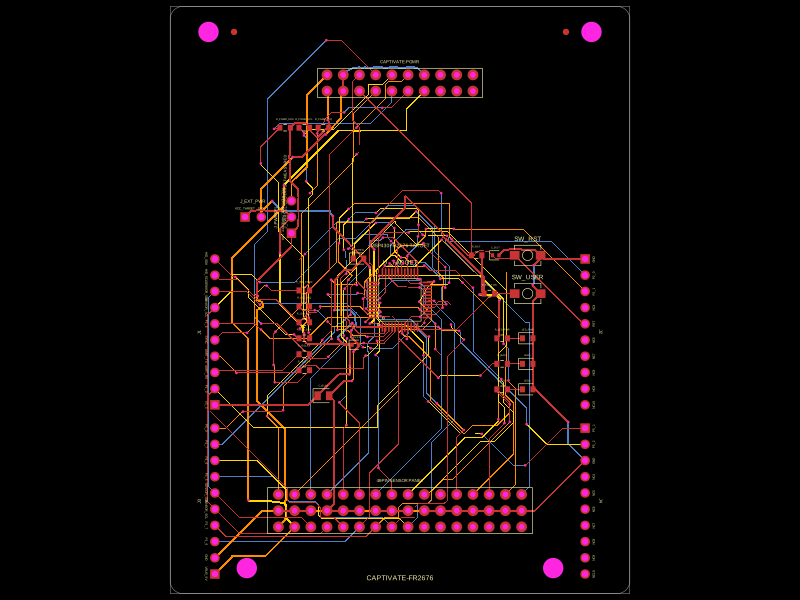 More from this authorShiboSoftwareDev/captivate-fr2676This circuit implements an MSP430FR2676 microcontroller-based development module with integrated power regulation, user interface components, programming interfaces, and sensor/boosterpack headers for embedded system prototyping.
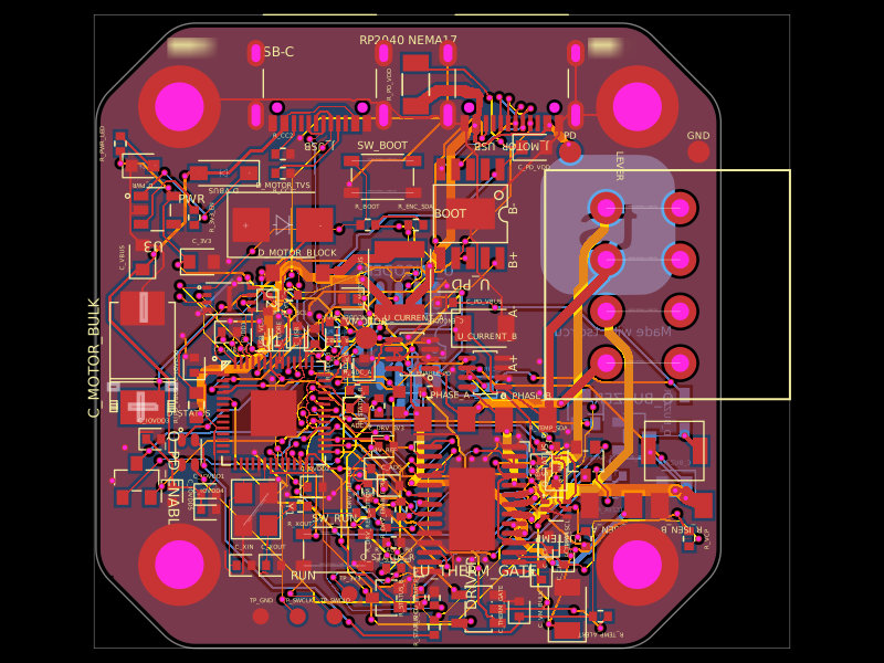 Similar packageastra/nema17-stepper-motor-controller-spring-clamp-rp2040A 4-layer RP2040 controller board that negotiates USB‑C PD motor power and drives a NEMA17 stepper via a DRV8825, with current sensing, thermal shutdown, RGB status LED, buzzer alarm, optional AS5600 encoder, protection/filtering, and test points.
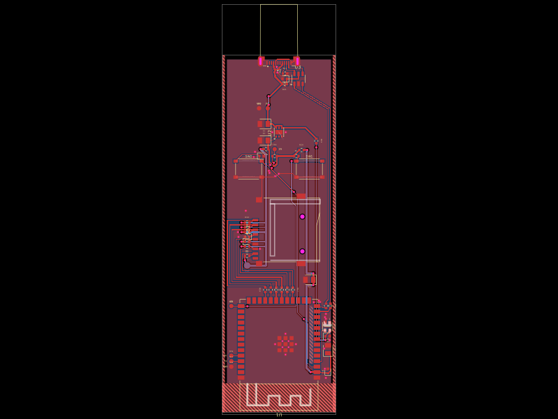 Discover something newpixalynx/esp32-usb-duckyA compact ESP32‑S3 USB‑C stick with native USB HID, 4‑bit microSD storage, 3.3V LDO power regulation, ESD protection, boot/reset controls, addressable RGB status LED, decoupling, and test pads.