seveibar/spi-display-webcam-interceptor
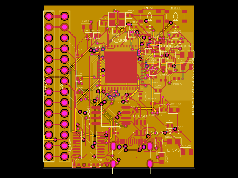
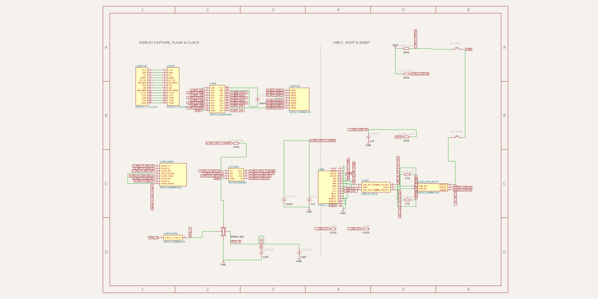
This collection of code defines various hardware components, including an crystal oscillator, microcontroller, voltage regulators, inductors, connectors, and logic gates, each represented with physical footprint, pin configurations, and 3D CAD models for PCB design and integration.
- Version
- 1.0.12
- License
- unset
- Stars
- 0
index.circuit.tsx
PCB
Schematic
import { SmdUsbC } from "@tsci/seveibar.smd-usb-c";
import { cloneElement, Fragment } from "react";
import { DFE201210U_2R2M_P2 } from "./imports/DFE201210U_2R2M_P2";
import { E3SB40E000030E } from "./imports/E3SB40E000030E";
import { ESP32_P4NRW32X } from "./imports/ESP32_P4NRW32X";
import { SKRPACE010 } from "./imports/SKRPACE010";
import { SN74LVC244APWR } from "./imports/SN74LVC244APWR";
import { TLV62569DRLR } from "./imports/TLV62569DRLR";
import { USBLC6_2SC6 } from "./imports/USBLC6_2SC6";
import { W25Q128JVSIQ } from "./imports/W25Q128JVSIQ";
import routingSolution from "./routing.json";
const sameCoordinate = (a: number, b: number) => Math.abs(a - b) < 1e-6;
const adjustedManufacturingRoutes = routingSolution.traces.map((trace) => ({
...trace,
route: trace.route.map((point) => {
const { pcb_trace_id: traceId } = trace;
if (point.x === undefined || point.y === undefined) return point;
// Separate the GPIO3/GPIO4 fanout traces where their simplified paths
// came within 0.08 mm of one another.
if (traceId === "source_trace_32_0") {
if (
sameCoordinate(point.x, -5.405161562950456) &&
sameCoordinate(point.y, 7.979797334841687)
) {
return { ...point, y: 7.949797334841687 };
}
if (
sameCoordinate(point.x, -5.103099546460042) &&
sameCoordinate(point.y, 7.96541620221355)
) {
return { ...point, y: 7.93541620221355 };
}
}
// Keep the shared button ground trace above SW_RESET's unconnected
// duplicate solder pad.
if (
traceId === "source_trace_136__source_net_0_mst45_0" &&
sameCoordinate(point.y, 18.10506536874412)
) {
return { ...point, y: 18.13506536874412 };
}
// Move the V3V3 link away from GPIO43 along the top edge of U_MCU.
if (
traceId ===
"source_trace_19__source_trace_37__source_trace_40__source_trace_43__source_trace_46__source_trace_49__source_trace_52__source_trace_59__source_trace_62__source_trace_78__source_trace_84__source_trace_86__source_trace_192__source_trace_195__source_net_1_mst13_0" &&
point.x > 2.88 &&
point.x < 2.91
) {
return { ...point, x: 2.8 };
}
// Bow the GPIO5 inner-layer segment around the existing GPIO7 via.
if (
traceId === "source_trace_33_0" &&
sameCoordinate(point.x, -5.026442511114322) &&
sameCoordinate(point.y, 7.457722681175604)
) {
return { ...point, x: -5.3, y: 7.45 };
}
// Give the PSRAM decoupling via more room outside the GPIO34 pad and the
// neighboring GPIO35/BOOT route.
if (
traceId ===
"source_trace_126__source_trace_127__source_trace_128__source_trace_130__source_trace_132_mst0_0" &&
sameCoordinate(point.x, 6.19058496529081) &&
sameCoordinate(point.y, 4.298298490400989)
) {
return { ...point, x: 6.25, y: 4.25 };
}
// Center the V1V2 via in the narrow channel between the exposed GND pad
// and the same-net VDD_HP_2 lead.
if (
traceId ===
"source_trace_65__source_trace_68__source_trace_71__source_trace_74__source_trace_95__source_trace_98__source_net_3_mst8_0" &&
sameCoordinate(point.x, 4.549993499999999) &&
sameCoordinate(point.y, 7.949992)
) {
return { ...point, x: 4.7 };
}
// Reuse the explicitly placed C_LDO ground via instead of dropping a
// second autorouted via only 0.125 mm away.
if (
traceId === "source_trace_136__source_net_0_mst53_0" &&
sameCoordinate(point.x, 8.3) &&
sameCoordinate(point.y, 8.075)
) {
if (point.route_type === "via") {
return {
route_type: "through_pad" as const,
start: { x: 8.3, y: 8.2 },
end: { x: 8.3, y: 8.2 },
start_layer: "inner1" as const,
end_layer: "top" as const,
width: 0.18,
};
}
return { ...point, x: 8.3, y: 8.2 };
}
return point;
}),
}));
const createFrozenManufacturingAutorouter = async () => {
const handlers: Record<string, (event: any) => void> = {};
return {
on(eventName: string, handler: (event: any) => void) {
handlers[eventName] = handler;
},
start() {
handlers.complete?.({ traces: adjustedManufacturingRoutes });
},
stop() {},
};
};
type SmdUsbCProps = Parameters<typeof SmdUsbC>[0];
const usbCPinAttributes = {
1: { requiresGround: true, mustBeConnected: true },
2: { requiresGround: true, mustBeConnected: true },
3: {
providesPower: true,
requiresPower: true,
providesVoltage: "5V",
requiresVoltage: "5V",
mustBeConnected: true,
},
4: {
providesPower: true,
requiresPower: true,
providesVoltage: "5V",
requiresVoltage: "5V",
mustBeConnected: true,
},
5: { doNotConnect: true },
6: { mustBeConnected: true },
7: { mustBeConnected: true },
8: { mustBeConnected: true },
9: { mustBeConnected: true },
10: { mustBeConnected: true },
11: { doNotConnect: true },
12: { mustBeConnected: true },
13: {
providesPower: true,
requiresPower: true,
providesVoltage: "5V",
requiresVoltage: "5V",
mustBeConnected: true,
},
14: {
providesPower: true,
requiresPower: true,
providesVoltage: "5V",
requiresVoltage: "5V",
mustBeConnected: true,
},
15: { requiresGround: true, mustBeConnected: true },
16: { requiresGround: true, mustBeConnected: true },
17: { requiresGround: true, mustBeConnected: true },
18: { requiresGround: true, mustBeConnected: true },
19: { requiresGround: true, mustBeConnected: true },
20: { requiresGround: true, mustBeConnected: true },
} as unknown as NonNullable<SmdUsbCProps["pinAttributes"]>;
/** Add the connector courtyard while arranging its built-in symbol. */
const SmdUsbCWithFixedSchematic = (props: SmdUsbCProps) => {
const usbC = SmdUsbC(props);
const footprintWithCourtyard = cloneElement(
usbC.props.footprint,
{},
usbC.props.footprint.props.children,
<courtyardoutline
outline={[
{ x: -5.18, y: -5.37 },
{ x: 5.18, y: -5.37 },
{ x: 5.18, y: 3.2 },
{ x: -5.18, y: 3.2 },
{ x: -5.18, y: -5.37 },
]}
/>,
);
return cloneElement(usbC, {
pinLabels: {
...usbC.props.pinLabels,
17: ["SHIELD1", "alt_0"],
18: ["SHIELD2", "alt_1"],
19: ["SHIELD3", "alt_2"],
20: ["SHIELD4", "alt_3"],
},
pinAttributes: props.pinAttributes ?? usbCPinAttributes,
footprint: footprintWithCourtyard,
schPortArrangement: {
leftSide: { pins: [], direction: "top-to-bottom" },
rightSide: {
pins: [
"GND1",
"GND2",
"VBUS1",
"VBUS2",
"DP1",
"DP2",
"DM1",
"DM2",
"CC1",
"CC2",
"SBU1",
"SBU2",
"SHIELD1",
"SHIELD2",
"SHIELD3",
"SHIELD4",
],
direction: "top-to-bottom",
},
},
schPinStyle: {},
});
};
const displayPinLabels = {
pin1: "VCC",
pin2: "GND",
pin3: "CS",
pin4: "RESET",
pin5: "DC_RS",
pin6: "SDI_MOSI",
pin7: "SCK",
pin8: "LED",
pin9: "SDO_MISO",
pin10: "T_CLK",
pin11: "T_CS",
pin12: "T_DIN",
pin13: "T_DO",
pin14: "T_IRQ",
} as const;
const displayPcbLabels = {
pin1: "VCC",
pin2: "GND",
pin3: "CS",
pin4: "RST",
pin5: "DC",
pin6: "MOSI",
pin7: "SCK",
pin8: "LED",
pin9: "MISO",
pin10: "TCLK",
pin11: "TCS",
pin12: "TDIN",
pin13: "TDO",
pin14: "TIRQ",
} as const;
/** Manufacturer-compatible 1x14 HCTL footprint in the board's vertical row. */
const DisplayHeaderFootprint = () => (
<footprint>
{Array.from({ length: 14 }, (_, index) => (
<Fragment key={`display-header-pad-${index + 1}`}>
<platedhole
portHints={[`pin${index + 1}`]}
pcbX={0}
pcbY={(6.5 - index) * 2.54}
outerDiameter="1.7mm"
holeDiameter="1.1mm"
shape="circle"
/>
</Fragment>
))}
<silkscreenrect
pcbX={0}
pcbY={0}
width="2.5mm"
height="35.56mm"
strokeWidth="0.2mm"
/>
<courtyardoutline
outline={[
{ x: -1.55, y: -18.31 },
{ x: 1.55, y: -18.31 },
{ x: 1.55, y: 18.31 },
{ x: -1.55, y: 18.31 },
{ x: -1.55, y: -18.31 },
]}
/>
</footprint>
);
const passThroughPins = Array.from({ length: 14 }, (_, index) => index + 1);
// GPIO1..GPIO8 form a compact capture bank. SPI clock/data/chip-select can use
// GP-SPI slave + GDMA; the other five signals are sampled as control inputs.
const captureChannels = [
{ headerPin: 3, bufferIn: 2, bufferOut: 18, mcuPin: 1 }, // GPIO1 LCD_CS
{ headerPin: 4, bufferIn: 4, bufferOut: 16, mcuPin: 2 }, // GPIO2 LCD_RESET
{ headerPin: 5, bufferIn: 6, bufferOut: 14, mcuPin: 3 }, // GPIO3 LCD_DC
{ headerPin: 6, bufferIn: 8, bufferOut: 12, mcuPin: 4 }, // GPIO4 LCD_MOSI
{ headerPin: 7, bufferIn: 11, bufferOut: 9, mcuPin: 5 }, // GPIO5 LCD_SCK
{ headerPin: 8, bufferIn: 13, bufferOut: 7, mcuPin: 6 }, // GPIO6 LCD_LED
{ headerPin: 9, bufferIn: 15, bufferOut: 5, mcuPin: 7 }, // GPIO7 LCD_MISO
{ headerPin: 14, bufferIn: 17, bufferOut: 3, mcuPin: 8 }, // GPIO8 TOUCH_IRQ
] as const;
const p4ThreeVThreePins = [9, 21, 62, 85, 96, 75, 77, 101, 102] as const;
const p4CorePins = [26, 54, 76, 91] as const;
const p4ThreeVThreeCaps = [
{ pin: 9, name: "C_LP", x: -9.2, y: 7.4 },
{ pin: 21, name: "C_IO0", x: -9.2, y: 1.9 },
{ pin: 62, name: "C_IO4", x: 8.1, y: 3.3 },
{ pin: 85, name: "C_IO5", x: 3.2, y: 12.2 },
{ pin: 96, name: "C_IO6", x: -0.5, y: 13 },
{ pin: 75, name: "C_LDO", x: 7.2, y: 8.2 },
{ pin: 77, name: "C_DCDCC", x: 8.5, y: 10.4 },
{ pin: 101, name: "C_ANA", x: -5, y: 12 },
{ pin: 102, name: "C_BAT_100N", x: -7, y: 12 },
] as const;
const p4CoreCaps = [
{ pin: 26, name: "C_HP0", x: -9.2, y: -1.5, rotation: 0 },
{ pin: 54, name: "C_HP1", x: 9.2, y: -1, rotation: 0 },
{ pin: 76, name: "C_HP2", x: 8.1, y: 9.3, rotation: 0 },
{ pin: 91, name: "C_HP3", x: 2.5, y: 11.2, rotation: 0 },
] as const;
type PlaneNet = "GND" | "V3V3" | "VBUS" | "V1V2";
type NetTraceProps = {
from: string;
net: PlaneNet;
width?: string;
maxViaCount?: number;
};
const NetTrace = ({ from, net, width, maxViaCount = 0 }: NetTraceProps) => (
<trace
from={from}
to={`net.${net}`}
width={width}
maxViaCount={maxViaCount}
/>
);
const McuPlaneDecoupler = ({
name,
targetPin,
x,
y,
rotation = 0,
powerNet,
schX,
schY,
}: {
name: string;
targetPin: number;
x: number;
y: number;
rotation?: number;
powerNet: "V3V3" | "V1V2";
schX: number;
schY: number;
}) => (
<>
<capacitor
name={name}
capacitance="100nF"
maxDecouplingTraceLength={10}
footprint="0402"
pcbX={x}
pcbY={y}
pcbRotation={rotation}
schSheetName="POWER"
schSectionName="MCU_POWER"
schX={schX}
schY={schY}
schOrientation="vertical"
/>
<trace
from={`.U_MCU > .pin${targetPin}`}
to={`.${name} > .pin1`}
width="0.18mm"
maxLength="10mm"
maxViaCount={0}
pcbPathRelativeTo={targetPin === 77 ? ".U_MCU > .pin77" : undefined}
pcbPath={
targetPin === 77
? [
".U_MCU > .pin77",
{ x: 5.9, y: 4.025 },
{ x: 5.9, y: 5.9 },
`.${name} > .pin1`,
]
: undefined
}
/>
<NetTrace from={`.${name} > .pin1`} net={powerNet} />
{targetPin === 75 ? (
<>
<via
name="C_LDO_GND_VIA"
pcbX={8.3}
pcbY={8.2}
holeDiameter="0.3mm"
outerDiameter="0.6mm"
connectsTo={[".C_LDO > .pin2", "net.GND"]}
/>
<trace
from=".C_LDO > .pin2"
to=".C_LDO_GND_VIA > .pin1"
width="0.18mm"
maxViaCount={0}
pcbPathRelativeTo=".C_LDO > .pin2"
pcbPath={[
".C_LDO > .pin2",
{ x: 0.59, y: 0 },
".C_LDO_GND_VIA > .pin1",
]}
/>
</>
) : targetPin === 76 ? (
<via
name="C_HP2_GND_VIA"
pcbX={9.2}
pcbY={9.3}
holeDiameter="0.3mm"
outerDiameter="0.6mm"
connectsTo={[".C_HP2 > .pin2", "net.GND"]}
/>
) : targetPin === 77 ? (
<via
name="C_DCDCC_GND_VIA"
pcbX={9.6}
pcbY={10.4}
holeDiameter="0.3mm"
outerDiameter="0.6mm"
connectsTo={[".C_DCDCC > .pin2", "net.GND"]}
/>
) : (
<NetTrace from={`.${name} > .pin2`} net="GND" />
)}
</>
);
export default () => (
<board
width="35.8mm"
height="38.74mm"
layers={4}
minViaHoleDiameter="0.3mm"
minViaPadDiameter="0.6mm"
autorouterEffortLevel="1x"
autorouter={{
traceClearance: "0.12mm",
algorithmFn: createFrozenManufacturingAutorouter,
}}
>
<net name="GND" isGroundNet />
<net name="V3V3" isPowerNet />
<net name="VBUS" isPowerNet />
<net name="V1V2" isPowerNet />
<schematicsheet
name="SIGNALS"
displayName="1. Display Capture, Memory & USB"
sheetIndex={0}
>
<schematicsection
name="CAPTURE_MEMORY"
displayName="Display Capture, Flash & Clock"
sectionTitleFontSize={0}
/>
<schematicsection
name="USB"
displayName="USB-C, Boot & Reset"
sectionTitleFontSize={0}
/>
<schematictext
text="DISPLAY CAPTURE, FLASH & CLOCK"
schX={-13.2}
schY={8.5}
fontSize={0.26}
anchor="left"
color="#555555"
/>
<schematictext
text="USB-C, BOOT & RESET"
schX={2.2}
schY={8.5}
fontSize={0.26}
anchor="left"
color="#555555"
/>
<schematicline
x1={1.2}
y1={-8.4}
x2={1.2}
y2={8.4}
strokeWidth={0.03}
color="#999999"
isDashed
/>
</schematicsheet>
<schematicsheet
name="POWER"
displayName="2. Power, Regulators & Decoupling"
sheetIndex={1}
>
<schematicsection name="MCU_POWER" displayName="ESP32-P4 Power" />
<schematicsection name="CORE_POWER" displayName="1.2 V Core Buck" />
<schematicsection
name="THREE_VOLT_POWER"
displayName="USB 5 V to 3.3 V Buck"
/>
</schematicsheet>
<pinheader
name="J_DISPLAY"
pinCount={14}
pitch="2.54mm"
gender="female"
supplierPartNumbers={{ jlcpcb: ["C2897377"] }}
manufacturerPartNumber="PM254-1-14-Z-8.5"
footprint={<DisplayHeaderFootprint />}
cadModel={{
objUrl:
"https://modelcdn.tscircuit.com/easyeda_models/assets/C2897377.obj?uuid=7ac80a5dae2842a19e077dc2a4340131",
stepUrl:
"https://modelcdn.tscircuit.com/easyeda_models/assets/C2897377.step?uuid=7ac80a5dae2842a19e077dc2a4340131",
pcbRotationOffset: -90,
modelOriginPosition: { x: 0, y: 0.0000127, z: -0.300006 },
}}
pcbX={-16.5}
pcbY={0}
schSheetName="SIGNALS"
schSectionName="CAPTURE_MEMORY"
schX={-13}
schY={5}
schWidth={0.96}
schFacingDirection="right"
pinLabels={displayPinLabels}
pcbPinLabels={displayPcbLabels}
showSilkscreenPinLabels
/>
<pinheader
name="J_HOST"
pinCount={14}
pitch="2.54mm"
gender="male"
supplierPartNumbers={{ jlcpcb: ["C2894937"] }}
manufacturerPartNumber="PZ254-1-14-Z-8.5"
footprint={<DisplayHeaderFootprint />}
cadModel={{
objUrl:
"https://modelcdn.tscircuit.com/easyeda_models/assets/C2894937.obj?uuid=08b06314cd6a40fe8bae6f2b80f3ecbb",
stepUrl:
"https://modelcdn.tscircuit.com/easyeda_models/assets/C2894937.step?uuid=08b06314cd6a40fe8bae6f2b80f3ecbb",
pcbRotationOffset: -90,
modelOriginPosition: { x: 0.0000632, y: 0.0000127, z: -0.000006 },
}}
pcbX={-12.8}
pcbY={0}
layer="bottom"
schSheetName="SIGNALS"
schSectionName="CAPTURE_MEMORY"
schX={-10.5}
schY={5}
schWidth={0.96}
schFacingDirection="left"
pinLabels={displayPinLabels}
pcbPinLabels={displayPcbLabels}
showSilkscreenPinLabels
/>
{passThroughPins.map((pin) => (
<trace
key={`pass-${pin}`}
from={`.J_HOST > .pin${pin}`}
to={`.J_DISPLAY > .pin${pin}`}
width={pin <= 2 ? "0.6mm" : "0.18mm"}
maxViaCount={pin <= 2 ? 0 : undefined}
pcbPath={
pin <= 2
? [`.J_HOST > .pin${pin}`, `.J_DISPLAY > .pin${pin}`]
: undefined
}
/>
))}
<NetTrace from=".J_HOST > .pin2" net="GND" width="0.18mm" />
<ESP32_P4NRW32X name="U_MCU" pcbX={0.5} pcbY={4.5} schHeight={10.6} />
<schematicbox
name="U_MCU_IO"
chipRef=".U_MCU"
schSheetName="SIGNALS"
schSectionName="CAPTURE_MEMORY"
schX={-0.5}
schY={4}
width={1.575}
height={1.8}
title="U_MCU Capture"
pinLabels={{
pin1: "GPIO1",
pin2: "GPIO2",
pin3: "GPIO3",
pin4: "GPIO4",
pin5: "GPIO5",
pin6: "GPIO6",
pin7: "GPIO7",
pin8: "GPIO8",
}}
schPinArrangement={{
leftSide: [
"pin1",
"pin2",
"pin3",
"pin4",
"pin5",
"pin6",
"pin7",
"pin8",
],
rightSide: [],
}}
/>
<schematicbox
name="U_MCU_PWR"
chipRef=".U_MCU"
schSheetName="POWER"
schSectionName="MCU_POWER"
schX={-11}
schY={0.5}
width={3.195}
height={2.2}
title="U_MCU Power"
pinLabels={{
pin1: "VDD_LP",
pin2: "VDD_IO_0",
pin3: "VDD_IO_4",
pin4: "VDD_IO_5",
pin5: "VDD_IO_6",
pin6: "VDD_LDO",
pin7: "VDD_DCDCC",
pin8: "VDD_ANA",
pin9: "VDD_BAT",
pin10: "VDD_HP_0",
pin11: "VDD_HP_1",
pin12: "VDD_HP_2",
pin13: "VDD_HP_3",
pin14: "VDD_PSRAM_0",
pin15: "VDD_PSRAM_1",
pin16: "VDDO_PSRAM",
pin17: "VDDO_3",
pin18: "VDDO_4",
pin19: "VDD_USBPHY",
pin20: "EN_DCDC",
pin21: "FB_DCDC",
pin22: "GND",
}}
schPinArrangement={{
leftSide: [
"pin1",
"pin2",
"pin3",
"pin4",
"pin5",
"pin6",
"pin7",
"pin8",
"pin9",
"pin19",
],
rightSide: [
"pin10",
"pin11",
"pin12",
"pin13",
"pin14",
"pin15",
"pin16",
"pin17",
"pin18",
"pin20",
"pin21",
"pin22",
],
}}
/>
<schematicbox
name="U_MCU_MEM"
chipRef=".U_MCU"
schSheetName="SIGNALS"
schSectionName="CAPTURE_MEMORY"
schX={-10.5}
schY={-2}
width={2.145}
height={1.8}
title="U_MCU Memory/Clock"
pinLabels={{
pin1: "FLASH_CS",
pin2: "FLASH_Q",
pin3: "FLASH_WP",
pin4: "VDD_FLASHIO",
pin5: "FLASH_HOLD",
pin6: "FLASH_CK",
pin7: "FLASH_D",
pin8: "VDDO_FLASH",
}}
schPinArrangement={{
leftSide: [
"pin1",
"pin2",
"pin3",
"pin4",
"pin5",
"pin6",
"pin7",
"pin8",
],
rightSide: [],
}}
/>
<schematicbox
name="U_MCU_XTAL"
chipRef=".U_MCU"
schSheetName="SIGNALS"
schSectionName="CAPTURE_MEMORY"
schX={-10.5}
schY={-7}
width={1.5}
height={0.4}
title="U_MCU XTAL"
pinLabels={{ pin1: "XTAL_N", pin2: "XTAL_P" }}
schPinArrangement={{ leftSide: ["pin1"], rightSide: ["pin2"] }}
/>
<schematicbox
name="U_MCU_USB_BOOT"
chipRef=".U_MCU"
schSheetName="SIGNALS"
schSectionName="USB"
schX={10.1}
schY={-3}
width={2.4}
height={0.6}
title="U_MCU USB/Boot"
pinLabels={{
pin1: "USB_DM",
pin2: "USB_DP",
pin3: "CHIP_PU",
pin4: "GPIO35",
pin5: "GPIO36",
}}
schPinArrangement={{
leftSide: ["pin1", "pin2"],
rightSide: ["pin3", "pin4", "pin5"],
}}
/>
<SN74LVC244APWR
name="U_BUF"
pcbX={-7.1}
pcbY={-13.8}
pcbRotation={90}
schSheetName="SIGNALS"
schSectionName="CAPTURE_MEMORY"
schX={-7}
schY={4}
/>
<NetTrace from=".U_BUF > .pin1" net="GND" />
<NetTrace from=".U_BUF > .pin10" net="GND" />
<NetTrace from=".U_BUF > .pin19" net="GND" />
<via
name="U_BUF_V3V3_VIA"
pcbX={-9.2}
pcbY={-16.7}
holeDiameter="0.3mm"
outerDiameter="0.6mm"
connectsTo={[".U_BUF > .pin20", "net.V3V3"]}
/>
<capacitor
name="C_BUF"
capacitance="100nF"
maxDecouplingTraceLength={8}
footprint="0402"
pcbX={-10}
pcbY={-18.5}
schSheetName="SIGNALS"
schSectionName="CAPTURE_MEMORY"
schX={-3.8}
schY={4}
schOrientation="vertical"
/>
<trace from=".C_BUF > .pin1" to=".U_BUF > .pin20" />
<NetTrace from=".C_BUF > .pin2" net="GND" />
{captureChannels.map((channel) => (
<trace
key={`tap-in-${channel.headerPin}`}
from={`.J_HOST > .pin${channel.headerPin}`}
to={`.U_BUF > .pin${channel.bufferIn}`}
width="0.18mm"
maxViaCount={channel.headerPin === 6 ? 2 : undefined}
pcbPath={
channel.headerPin === 6
? [
`.J_HOST > .pin${channel.headerPin}`,
{ x: 1.5, y: 3.81 },
{
x: 1.5,
y: 3.81,
via: true,
fromLayer: "top",
toLayer: "inner1",
},
{ x: 1.5, y: 3.81 },
{ x: 1.5, y: -10.5 },
{ x: 9.6, y: -12.175 },
{
x: 9.6,
y: -12.175,
via: true,
fromLayer: "inner1",
toLayer: "top",
},
{ x: 9.6, y: -12.175 },
`.U_BUF > .pin${channel.bufferIn}`,
]
: undefined
}
/>
))}
{captureChannels.map((channel) => (
<trace
key={`tap-out-${channel.headerPin}`}
from={`.U_BUF > .pin${channel.bufferOut}`}
to={`.U_MCU > .pin${channel.mcuPin}`}
width="0.1mm"
maxViaCount={
channel.mcuPin === 6 || channel.mcuPin === 8
? 0
: channel.mcuPin === 7
? 0
: undefined
}
pcbPath={
channel.mcuPin === 6
? [
`.U_BUF > .pin${channel.bufferOut}`,
{ x: 0.975, y: -3.9 },
{ x: 0.975, y: -0.1 },
{ x: 20.925, y: -0.1 },
`.U_MCU > .pin${channel.mcuPin}`,
]
: channel.mcuPin === 8
? [
`.U_BUF > .pin${channel.bufferOut}`,
{ x: -1.625, y: -4.6 },
{ x: 3.5, y: -4.6 },
{ x: 3.5, y: -0.35 },
{ x: 20.225, y: -0.35 },
`.U_MCU > .pin${channel.mcuPin}`,
]
: undefined
}
/>
))}
{p4ThreeVThreeCaps.map((cap, index) => (
<McuPlaneDecoupler
key={cap.name}
name={cap.name}
targetPin={cap.pin}
x={cap.x}
y={cap.y}
powerNet="V3V3"
schX={-12 + index * 2.3}
schY={8}
/>
))}
{p4CoreCaps.map((cap, index) => (
<McuPlaneDecoupler
key={cap.name}
name={cap.name}
targetPin={cap.pin}
x={cap.x}
y={cap.y}
rotation={cap.rotation}
powerNet="V1V2"
schX={-12 + index * 2.8}
schY={5.5}
/>
))}
<NetTrace from=".U_MCU > .pin105" net="GND" width="0.18mm" />
<capacitor
name="C_LDO_BULK"
capacitance="10uF"
maxDecouplingTraceLength={10}
footprint="0603"
pcbX={10.42}
pcbY={5.2}
pcbRotation={-90}
schSheetName="POWER"
schSectionName="MCU_POWER"
schX={9}
schY={8}
schOrientation="vertical"
/>
<trace
from=".U_MCU > .pin75"
to=".C_LDO_BULK > .pin1"
width="0.18mm"
maxLength="10mm"
/>
<NetTrace from=".C_LDO_BULK > .pin1" net="V3V3" width="0.18mm" />
<via
name="C_LDO_BULK_GND_VIA"
pcbX={10.42}
pcbY={3.55}
holeDiameter="0.3mm"
outerDiameter="0.6mm"
connectsTo={[".C_LDO_BULK > .pin2", "net.GND"]}
/>
<capacitor
name="C_DCDCC_BULK"
capacitance="10uF"
maxDecouplingTraceLength={10}
footprint="0603"
pcbX={10.42}
pcbY={9.7}
pcbRotation={90}
schSheetName="POWER"
schSectionName="MCU_POWER"
schX={11.5}
schY={6.5}
schOrientation="vertical"
/>
<trace
from=".U_MCU > .pin77"
to=".C_DCDCC_BULK > .pin1"
width="0.18mm"
maxLength="10mm"
maxViaCount={0}
pcbPathRelativeTo=".U_MCU > .pin77"
pcbPath={[
".U_MCU > .pin77",
{ x: 6.3, y: 4.025 },
{ x: 6.3, y: 4.25 },
{ x: 9.1, y: 4.25 },
{ x: 9.1, y: 4.375 },
".C_DCDCC_BULK > .pin1",
]}
/>
<NetTrace from=".C_DCDCC_BULK > .pin1" net="V3V3" width="0.18mm" />
<via
name="C_DCDCC_BULK_GND_VIA"
pcbX={10.42}
pcbY={11.35}
holeDiameter="0.3mm"
outerDiameter="0.6mm"
connectsTo={[".C_DCDCC_BULK > .pin2", "net.GND"]}
/>
<capacitor
name="C_BAT_BULK"
capacitance="10uF"
maxDecouplingTraceLength={10}
footprint="0603"
pcbX={-7.5}
pcbY={14}
schSheetName="POWER"
schSectionName="MCU_POWER"
schX={11.5}
schY={8}
schOrientation="vertical"
/>
<trace from=".C_BAT_BULK > .pin1" to=".C_BAT_100N > .pin1" />
<NetTrace from=".C_BAT_BULK > .pin2" net="GND" />
<TLV62569DRLR
name="U_CORE_BUCK"
pcbX={12.4}
pcbY={7.5}
schSheetName="POWER"
schSectionName="CORE_POWER"
schX={-11}
schY={-4.5}
/>
<DFE201210U_2R2M_P2
name="L_CORE"
pcbX={15.8}
pcbY={7.5}
schSheetName="POWER"
schSectionName="CORE_POWER"
schX={-7}
schY={-4.5}
/>
<capacitor
name="C_CORE_IN"
capacitance="4.7uF"
maxDecouplingTraceLength={10}
footprint="0603"
pcbX={12}
pcbY={4.2}
pcbRotation={-90}
schSheetName="POWER"
schSectionName="CORE_POWER"
schX={-11}
schY={-7.5}
schOrientation="vertical"
/>
<capacitor
name="C_CORE_OUT"
capacitance="22uF"
maxDecouplingTraceLength={10}
footprint="0805"
pcbX={16}
pcbY={4.5}
schSheetName="POWER"
schSectionName="CORE_POWER"
schX={-3}
schY={-4.5}
schOrientation="vertical"
/>
<resistor
name="R_CORE_TOP"
resistance="499kohm"
footprint="0402"
pcbX={12.4}
pcbY={10.5}
schSheetName="POWER"
schSectionName="CORE_POWER"
schX={-7}
schY={-7.5}
/>
<resistor
name="R_CORE_BOT"
resistance="499kohm"
footprint="0402"
pcbX={14.4}
pcbY={10.5}
schSheetName="POWER"
schSectionName="CORE_POWER"
schX={-3}
schY={-7.5}
/>
<capacitor
name="C_CORE_FB"
capacitance="22pF"
maxDecouplingTraceLength={10}
footprint="0402"
pcbX={13.4}
pcbY={12}
schSheetName="POWER"
schSectionName="CORE_POWER"
schX={-5}
schY={-8.8}
schOrientation="vertical"
/>
<trace from=".U_CORE_BUCK > .pin3" to=".C_CORE_IN > .pin1" width="0.18mm" />
<NetTrace from=".C_CORE_IN > .pin1" net="V3V3" width="0.18mm" />
<NetTrace from=".U_CORE_BUCK > .pin2" net="GND" width="0.15mm" />
<NetTrace from=".U_CORE_BUCK > .pin6" net="GND" width="0.15mm" />
<NetTrace from=".C_CORE_IN > .pin2" net="GND" />
<trace from=".U_MCU > .pin79" to=".U_CORE_BUCK > .pin5" width="0.15mm" />
<trace from=".U_MCU > .pin78" to=".U_CORE_BUCK > .pin1" width="0.15mm" />
<trace from=".U_CORE_BUCK > .pin4" to=".L_CORE > .pin1" width="0.18mm" />
<trace
from=".L_CORE > .pin2"
to=".C_CORE_OUT > .pin1"
width="0.5mm"
maxViaCount={0}
pcbPath={[".L_CORE > .pin2", ".C_CORE_OUT > .pin1"]}
/>
<trace from=".L_CORE > .pin2" to=".R_CORE_TOP > .pin1" />
<trace from=".R_CORE_TOP > .pin2" to=".R_CORE_BOT > .pin1" />
<trace from=".R_CORE_TOP > .pin2" to=".U_MCU > .pin78" />
<trace from=".C_CORE_FB > .pin1" to=".R_CORE_TOP > .pin1" />
<trace from=".C_CORE_FB > .pin2" to=".R_CORE_TOP > .pin2" />
<NetTrace from=".R_CORE_BOT > .pin2" net="GND" />
<NetTrace from=".C_CORE_OUT > .pin1" net="V1V2" width="0.18mm" />
<NetTrace from=".C_CORE_OUT > .pin2" net="GND" width="0.18mm" />
<W25Q128JVSIQ
name="U_FLASH"
pcbX={-1.9}
pcbY={-6.8}
pcbRotation={90}
schSheetName="SIGNALS"
schSectionName="CAPTURE_MEMORY"
schX={-5.5}
schY={-2}
/>
<trace from=".U_FLASH > .pin1" to=".U_MCU > .pin27" width="0.1mm" />
<trace from=".U_FLASH > .pin2" to=".U_MCU > .pin28" width="0.1mm" />
<trace from=".U_FLASH > .pin3" to=".U_MCU > .pin29" width="0.1mm" />
<trace from=".U_FLASH > .pin5" to=".U_MCU > .pin33" width="0.1mm" />
<trace from=".U_FLASH > .pin6" to=".U_MCU > .pin32" width="0.1mm" />
<trace from=".U_FLASH > .pin7" to=".U_MCU > .pin31" width="0.1mm" />
<trace from=".U_MCU > .pin71" to=".U_MCU > .pin30" width="0.18mm" />
<trace from=".U_MCU > .pin30" to=".U_FLASH > .pin8" width="0.18mm" />
<resistor
name="R_FLASH_CS"
resistance="10kohm"
footprint="0402"
pcbX={-0.8}
pcbY={-11}
schSheetName="SIGNALS"
schSectionName="CAPTURE_MEMORY"
schX={-5.5}
schY={0.5}
/>
<trace from=".R_FLASH_CS > .pin1" to=".U_FLASH > .pin8" />
<trace from=".R_FLASH_CS > .pin2" to=".U_FLASH > .pin1" />
<capacitor
name="C_FLASH"
capacitance="100nF"
maxDecouplingTraceLength={10}
footprint="0402"
pcbX={3.8}
pcbY={-6}
schSheetName="SIGNALS"
schSectionName="CAPTURE_MEMORY"
schX={-1.7}
schY={-4}
schOrientation="vertical"
/>
<trace from=".C_FLASH > .pin1" to=".U_FLASH > .pin8" />
<NetTrace from=".U_FLASH > .pin4" net="GND" />
<NetTrace from=".C_FLASH > .pin2" net="GND" />
<capacitor
name="C_FLASHIO_1U"
capacitance="1uF"
maxDecouplingTraceLength={10}
footprint="0402"
pcbX={1.2}
pcbY={-2.7}
schSheetName="SIGNALS"
schSectionName="CAPTURE_MEMORY"
schX={0.3}
schY={-4}
schOrientation="vertical"
/>
<trace
from=".C_FLASHIO_1U > .pin1"
to=".U_MCU > .pin30"
width="0.1mm"
maxViaCount={0}
/>
<NetTrace from=".C_FLASHIO_1U > .pin2" net="GND" />
<E3SB40E000030E
name="Y1"
pcbX={-0.5}
pcbY={15.8}
schSheetName="SIGNALS"
schSectionName="CAPTURE_MEMORY"
schX={-6.5}
schY={-6.5}
/>
<capacitor
name="C_XTAL_P"
capacitance="12pF"
maxDecouplingTraceLength={10}
footprint="0402"
pcbX={-3.6}
pcbY={14.9}
schSheetName="SIGNALS"
schSectionName="CAPTURE_MEMORY"
schX={-3.5}
schY={-8.2}
schOrientation="vertical"
/>
<capacitor
name="C_XTAL_N"
capacitance="12pF"
maxDecouplingTraceLength={10}
footprint="0402"
pcbX={2.6}
pcbY={16.7}
schSheetName="SIGNALS"
schSectionName="CAPTURE_MEMORY"
schX={-0.5}
schY={-8.2}
schOrientation="vertical"
/>
<trace
name="XTAL_P"
from=".U_MCU > .pin100"
to=".Y1 > .pin1"
width="0.15mm"
maxLength="10mm"
maxViaCount={0}
pcbPath={[
".U_MCU > .pin100",
{ x: -2.975, y: 6.5 },
{ x: -2.975, y: 7.5 },
".Y1 > .pin1",
]}
/>
<trace
name="XTAL_N"
from=".U_MCU > .pin99"
to=".Y1 > .pin3"
width="0.15mm"
maxLength="10mm"
maxViaCount={0}
pcbPath={[
".U_MCU > .pin99",
{ x: -2.625, y: 6 },
{ x: 1, y: 8.5 },
{ x: 1, y: 12.15 },
".Y1 > .pin3",
]}
/>
<trace from=".C_XTAL_P > .pin1" to=".Y1 > .pin1" />
<trace from=".C_XTAL_N > .pin1" to=".Y1 > .pin3" />
<NetTrace from=".Y1 > .pin2" net="GND" />
<NetTrace from=".Y1 > .pin4" net="GND" />
<NetTrace from=".C_XTAL_P > .pin2" net="GND" />
<NetTrace from=".C_XTAL_N > .pin2" net="GND" />
<trace from=".U_MCU > .pin72" to=".U_MCU > .pin59" />
<trace from=".U_MCU > .pin72" to=".U_MCU > .pin67" />
{[
{ name: "C_PSRAM0", x: 8.1, y: 2.2, value: "100nF", target: 59 },
{ name: "C_PSRAM1", x: 7.75, y: 5.0, value: "100nF", target: 67 },
{ name: "C_PSRAM_BULK", x: 10.4, y: 1.5, value: "1uF", target: 72 },
].map((cap, index) => (
<Fragment key={cap.name}>
<capacitor
name={cap.name}
capacitance={cap.value}
maxDecouplingTraceLength={10}
footprint="0402"
pcbX={cap.x}
pcbY={cap.y}
schSheetName="POWER"
schSectionName="MCU_POWER"
schX={index * 2.8}
schY={5.5}
schOrientation="vertical"
/>
<trace
from={`.${cap.name} > .pin1`}
to={`.U_MCU > .pin${cap.target}`}
maxViaCount={0}
/>
<NetTrace from={`.${cap.name} > .pin2`} net="GND" />
</Fragment>
))}
<capacitor
name="C_VOUT3"
capacitance="1uF"
maxDecouplingTraceLength={10}
footprint="0402"
pcbX={9.2}
pcbY={5.75}
pcbRotation={-90}
schSheetName="POWER"
schSectionName="MCU_POWER"
schX={8.4}
schY={5.5}
schOrientation="vertical"
/>
<capacitor
name="C_VOUT4"
capacitance="1uF"
maxDecouplingTraceLength={10}
footprint="0402"
pcbX={9.05}
pcbY={7.65}
pcbRotation={-90}
schSheetName="POWER"
schSectionName="MCU_POWER"
schX={11.2}
schY={5.5}
schOrientation="vertical"
/>
<trace
from=".C_VOUT3 > .pin1"
to=".U_MCU > .pin73"
maxLength="6mm"
maxViaCount={0}
pcbPath={[
".C_VOUT3 > .pin1",
{ x: -0.56, y: -2.6 },
{ x: -1.375, y: -2.6 },
".U_MCU > .pin73",
]}
/>
<trace
from=".C_VOUT4 > .pin1"
to=".U_MCU > .pin74"
maxLength="6mm"
maxViaCount={0}
pcbPath={[
".C_VOUT4 > .pin1",
{ x: -0.51, y: 0.7 },
{ x: 0.05, y: 0.7 },
{ x: 0.05, y: -2.35 },
".U_MCU > .pin74",
]}
/>
{/* Keep the VOUT3 return on the existing C_LDO ground via to avoid a
ground-via collision with the adjacent V3V3 escape. */}
<trace
name="C_VOUT3_GND_RETURN"
from=".C_VOUT3 > .pin2"
to=".C_LDO_GND_VIA > .pin1"
width="0.18mm"
maxViaCount={0}
/>
<NetTrace from=".C_VOUT4 > .pin2" net="GND" />
<resistor
name="R_USBPHY"
resistance="0ohm"
footprint="0402"
pcbX={8}
pcbY={-4}
schSheetName="POWER"
schSectionName="MCU_POWER"
schX={3.51}
schY={2.5}
/>
<NetTrace from=".R_USBPHY > .pin1" net="V3V3" />
<trace
from=".R_USBPHY > .pin2"
to=".U_MCU > .pin51"
maxViaCount={0}
pcbPath={[
".R_USBPHY > .pin2",
{ x: 1.5, y: 0 },
{ x: 1.5, y: 0.5 },
{ x: -2.4, y: 0.5 },
{ x: -2.4, y: 2.8 },
{ x: -3.475, y: 2.8 },
".U_MCU > .pin51",
]}
/>
{[
{ name: "C_USBPHY_10N", value: "10nF", x: 8.5, y: -5.5 },
{ name: "C_USBPHY_100N", value: "100nF", x: 10.5, y: -5.5 },
{ name: "C_USBPHY_4U7", value: "4.7uF", x: 13, y: -5.5 },
].map((cap, index) => (
<Fragment key={cap.name}>
<capacitor
name={cap.name}
capacitance={cap.value}
maxDecouplingTraceLength={10}
footprint={index === 2 ? "0603" : "0402"}
pcbX={cap.x}
pcbY={cap.y}
schSheetName="POWER"
schSectionName="MCU_POWER"
schX={index === 0 ? 6.5 : 6.4 + index * 2.8}
schY={2.5}
schOrientation="vertical"
/>
<trace
from={`.${cap.name} > .pin1`}
to=".R_USBPHY > .pin2"
maxViaCount={0}
/>
{index === 2 ? (
<NetTrace from={`.${cap.name} > .pin2`} net="GND" />
) : index === 0 ? (
<NetTrace from={`.${cap.name} > .pin2`} net="GND" />
) : (
<NetTrace from={`.${cap.name} > .pin2`} net="GND" />
)}
</Fragment>
))}
<USBLC6_2SC6
name="U_ESD"
pcbX={5.1}
pcbY={-9.7}
schSheetName="SIGNALS"
schSectionName="USB"
schX={5.6}
schY={-3}
/>
{/* The USBLC6 channels are interchangeable. Assigning DM to its left
channel and DP to its right channel preserves lane order on the PCB. */}
<trace from=".J_USB > .pin7" to=".U_ESD > .pin1" width="0.18mm" />
<trace
name="USB_HS_DM_CONN"
from=".J_USB > .pin9"
to=".U_ESD > .pin1"
width="0.18mm"
/>
<trace from=".J_USB > .pin8" to=".U_ESD > .pin3" width="0.18mm" />
<trace
name="USB_HS_DP_CONN"
from=".J_USB > .pin10"
to=".U_ESD > .pin3"
width="0.18mm"
/>
<resistor
name="R_USB_DP"
resistance="27ohm"
footprint="0402"
pcbX={5}
pcbY={-2.3}
pcbRotation={90}
schSheetName="SIGNALS"
schSectionName="USB"
schX={8.1}
schY={-2}
/>
<resistor
name="R_USB_DM"
resistance="27ohm"
footprint="0402"
pcbX={2.7}
pcbY={-2.3}
pcbRotation={90}
schSheetName="SIGNALS"
schSectionName="USB"
schX={8.1}
schY={-4}
/>
<trace
name="USB_HS_DM_POST_ESD"
from=".U_ESD > .pin6"
to=".R_USB_DM > .pin1"
width="0.18mm"
maxViaCount={0}
pcbPath={[
".U_ESD > .pin6",
{ x: -0.95, y: 1.8 },
{ x: 0, y: 2.4 },
{ x: 0, y: 5 },
{ x: -1.45, y: 6.5 },
".R_USB_DM > .pin1",
]}
/>
<trace
name="USB_HS_DP_POST_ESD"
from=".U_ESD > .pin4"
to=".R_USB_DP > .pin1"
width="0.18mm"
maxViaCount={0}
pcbPath={[
".U_ESD > .pin4",
{ x: 0.95, y: 1.8 },
{ x: 1.64, y: 3.4 },
{ x: 1.1, y: 5 },
{ x: -0.45, y: 6.5 },
".R_USB_DP > .pin1",
]}
/>
<trace
name="USB_HS_DM_MCU"
from=".R_USB_DM > .pin2"
to=".U_MCU > .pin49"
width="0.1mm"
maxViaCount={0}
pcbPathRelativeTo=".R_USB_DM > .pin2"
pcbPath={[".R_USB_DM > .pin2", { x: 1.1, y: -1.125 }, ".U_MCU > .pin49"]}
/>
<trace
name="USB_HS_DP_MCU"
from=".R_USB_DP > .pin2"
to=".U_MCU > .pin50"
width="0.1mm"
maxViaCount={0}
pcbPathRelativeTo=".R_USB_DP > .pin2"
pcbPath={[".R_USB_DP > .pin2", { x: 1.1, y: 0.825 }, ".U_MCU > .pin50"]}
/>
<SKRPACE010
name="SW_BOOT"
pcbX={13.3}
pcbY={16.5}
schSheetName="SIGNALS"
schSectionName="USB"
schX={12}
schY={8}
/>
<resistor
name="R_BOOT_PU"
resistance="10kohm"
footprint="0402"
pcbX={13.3}
pcbY={14}
schSheetName="SIGNALS"
schSectionName="USB"
schX={8}
schY={8}
/>
<NetTrace from=".R_BOOT_PU > .pin1" net="V3V3" />
<trace from=".R_BOOT_PU > .pin2" to=".U_MCU > .pin66" />
<trace from=".U_MCU > .pin66" to=".SW_BOOT > .pin1" />
<NetTrace from=".SW_BOOT > .pin2" net="GND" />
<resistor
name="R_GPIO36_PU"
resistance="10kohm"
footprint="0402"
pcbX={13.5}
pcbY={1.8}
schSheetName="SIGNALS"
schSectionName="USB"
schX={8}
schY={6}
/>
<NetTrace from=".R_GPIO36_PU > .pin1" net="V3V3" />
<trace
from=".R_GPIO36_PU > .pin2"
to=".U_MCU > .pin68"
maxViaCount={2}
pcbPath={[
".R_GPIO36_PU > .pin2",
{ x: 1.5, y: 0 },
{
x: 1.5,
y: 0,
via: true,
fromLayer: "top",
toLayer: "inner1",
},
{ x: 1.5, y: 0 },
{ x: 1.5, y: 3.575 },
{ x: -7.1, y: 3.575 },
{
x: -7.1,
y: 3.575,
via: true,
fromLayer: "inner1",
toLayer: "top",
},
{ x: -7.1, y: 3.575 },
".U_MCU > .pin68",
]}
/>
<SKRPACE010
name="SW_RESET"
pcbX={7.2}
pcbY={16.5}
schSheetName="SIGNALS"
schSectionName="USB"
schX={12}
schY={1}
/>
<resistor
name="R_RESET_PU"
resistance="10kohm"
footprint="0402"
pcbX={7.2}
pcbY={14}
schSheetName="SIGNALS"
schSectionName="USB"
schX={8}
schY={1}
/>
<capacitor
name="C_RESET"
capacitance="1uF"
maxDecouplingTraceLength={20}
footprint="0402"
pcbX={3.5}
pcbY={14}
schSheetName="SIGNALS"
schSectionName="USB"
schX={5}
schY={1}
schOrientation="vertical"
/>
<NetTrace from=".R_RESET_PU > .pin1" net="V3V3" />
<trace from=".C_RESET > .pin1" to=".U_MCU > .pin103" maxLength="20mm" />
<trace from=".R_RESET_PU > .pin2" to=".C_RESET > .pin1" />
<trace from=".R_RESET_PU > .pin2" to=".SW_RESET > .pin1" />
<NetTrace from=".C_RESET > .pin2" net="GND" />
<NetTrace from=".SW_RESET > .pin2" net="GND" />
<SmdUsbCWithFixedSchematic
name="J_USB"
pcbX={2.95}
pcbY={-15.46}
schSheetName="SIGNALS"
schSectionName="USB"
schX={1.8}
schY={-3}
schWidth={1.575}
schHeight={2.6}
/>
<trace
from=".J_USB > .pin2"
to=".J_USB > .pin1"
width="0.5mm"
maxViaCount={0}
pcbPath={[".J_USB > .pin2", ".J_USB > .pin1"]}
/>
<trace
from=".J_USB > .pin16"
to=".J_USB > .pin15"
width="0.5mm"
maxViaCount={0}
pcbPath={[".J_USB > .pin16", ".J_USB > .pin15"]}
/>
<NetTrace from=".J_USB > .pin1" net="GND" width="0.18mm" />
<NetTrace from=".J_USB > .pin15" net="GND" width="0.18mm" />
{[17, 18, 19, 20].map((pin) => (
<NetTrace
key={`usb-shield-gnd-${pin}`}
from={`.J_USB > .pin${pin}`}
net="GND"
width="0.18mm"
/>
))}
{[3, 4, 13, 14].map((pin) => (
<NetTrace
key={`usb-vbus-${pin}`}
from={`.J_USB > .pin${pin}`}
net="VBUS"
width="0.18mm"
/>
))}
<resistor
name="R_CC1"
resistance="5.1kohm"
footprint="0402"
pcbX={-4.5}
pcbY={-18.5}
schSheetName="SIGNALS"
schSectionName="USB"
schX={2.2}
schY={-6.3}
/>
<resistor
name="R_CC2"
resistance="5.1kohm"
footprint="0402"
pcbX={-6.5}
pcbY={-18.5}
schSheetName="SIGNALS"
schSectionName="USB"
schX={4.8}
schY={-6.3}
/>
<trace from=".J_USB > .pin6" to=".R_CC1 > .pin1" />
<via
name="R_CC1_GND_VIA"
pcbX={-2.8}
pcbY={-18.5}
holeDiameter="0.3mm"
outerDiameter="0.6mm"
connectsTo={[".R_CC1 > .pin2", "net.GND"]}
/>
<trace
from=".J_USB > .pin12"
to=".R_CC2 > .pin1"
maxViaCount={0}
pcbPath={[
".J_USB > .pin12",
{ x: 1.15, y: -1.34 },
{ x: -5.95, y: -1.34 },
{ x: -5.95, y: -1.84 },
{ x: -9.96, y: -1.84 },
".R_CC2 > .pin1",
]}
/>
<via
name="R_CC2_GND_VIA"
pcbX={-8.2}
pcbY={-18.5}
holeDiameter="0.3mm"
outerDiameter="0.6mm"
connectsTo={[".R_CC2 > .pin2", "net.GND"]}
/>
<NetTrace from=".U_ESD > .pin2" net="GND" />
<via
name="U_ESD_VBUS_VIA"
pcbX={6.8}
pcbY={-11.7}
holeDiameter="0.3mm"
outerDiameter="0.6mm"
connectsTo={[".U_ESD > .pin5", "net.VBUS"]}
/>
<TLV62569DRLR
name="U_3V3_BUCK"
pcbX={9.4}
pcbY={-13}
schSheetName="POWER"
schSectionName="THREE_VOLT_POWER"
schX={2}
schY={-4.5}
/>
<DFE201210U_2R2M_P2
name="L_3V3"
pcbX={12.8}
pcbY={-13}
schSheetName="POWER"
schSectionName="THREE_VOLT_POWER"
schX={6}
schY={-4.5}
/>
<capacitor
name="C_3V3_IN"
capacitance="4.7uF"
maxDecouplingTraceLength={10}
footprint="0603"
pcbX={10}
pcbY={-17}
pcbRotation={-90}
schSheetName="POWER"
schSectionName="THREE_VOLT_POWER"
schX={2}
schY={-7.5}
schOrientation="vertical"
/>
<capacitor
name="C_3V3_OUT"
capacitance="22uF"
maxDecouplingTraceLength={10}
footprint="0805"
pcbX={16}
pcbY={-15.5}
schSheetName="POWER"
schSectionName="THREE_VOLT_POWER"
schX={11}
schY={-4.5}
schOrientation="vertical"
/>
<resistor
name="R_3V3_TOP"
resistance="453kohm"
footprint="0402"
pcbX={12}
pcbY={-10.7}
schSheetName="POWER"
schSectionName="THREE_VOLT_POWER"
schX={6}
schY={-7.5}
/>
<resistor
name="R_3V3_BOT"
resistance="100kohm"
footprint="0402"
pcbX={14}
pcbY={-10.7}
schSheetName="POWER"
schSectionName="THREE_VOLT_POWER"
schX={11}
schY={-7.5}
/>
<capacitor
name="C_3V3_FB"
capacitance="22pF"
maxDecouplingTraceLength={10}
footprint="0402"
pcbX={12}
pcbY={-9.2}
schSheetName="POWER"
schSectionName="THREE_VOLT_POWER"
schX={8.5}
schY={-8.8}
schOrientation="vertical"
/>
<trace from=".U_3V3_BUCK > .pin3" to=".C_3V3_IN > .pin1" width="0.18mm" />
<NetTrace from=".U_3V3_BUCK > .pin5" net="VBUS" width="0.15mm" />
<NetTrace from=".C_3V3_IN > .pin1" net="VBUS" width="0.18mm" />
<NetTrace from=".U_3V3_BUCK > .pin2" net="GND" width="0.15mm" />
<NetTrace from=".U_3V3_BUCK > .pin6" net="GND" width="0.15mm" />
<NetTrace from=".C_3V3_IN > .pin2" net="GND" />
<trace from=".U_3V3_BUCK > .pin4" to=".L_3V3 > .pin1" width="0.18mm" />
<trace
from=".L_3V3 > .pin2"
to=".C_3V3_OUT > .pin1"
width="0.6mm"
maxViaCount={0}
pcbPath={[".L_3V3 > .pin2", ".C_3V3_OUT > .pin1"]}
/>
<trace from=".L_3V3 > .pin2" to=".R_3V3_TOP > .pin1" />
<trace from=".R_3V3_TOP > .pin2" to=".R_3V3_BOT > .pin1" />
<trace from=".R_3V3_TOP > .pin2" to=".U_3V3_BUCK > .pin1" width="0.15mm" />
<trace from=".C_3V3_FB > .pin1" to=".R_3V3_TOP > .pin1" />
<trace from=".C_3V3_FB > .pin2" to=".R_3V3_TOP > .pin2" />
<NetTrace from=".R_3V3_BOT > .pin2" net="GND" />
<NetTrace from=".C_3V3_OUT > .pin1" net="V3V3" width="0.18mm" />
<NetTrace from=".C_3V3_OUT > .pin2" net="GND" width="0.18mm" />
<silkscreentext
text="ESP32-P4 SPI DISPLAY UVC CAPTURE"
pcbX={17.3}
pcbY={0}
pcbRotation={90}
fontSize="0.7mm"
anchorAlignment="center"
/>
<silkscreentext
text="DISPLAY"
pcbX={-17.3}
pcbY={0}
pcbRotation={90}
fontSize="1mm"
anchorAlignment="center"
/>
<silkscreentext
text="HOST"
pcbX={-13.5}
pcbY={0}
pcbRotation={90}
fontSize="1mm"
anchorAlignment="center"
/>
<silkscreentext
text="BOOT"
pcbX={13.2}
pcbY={18.5}
fontSize="0.9mm"
anchorAlignment="center"
/>
<silkscreentext
text="RESET"
pcbX={7.5}
pcbY={18.5}
fontSize="0.9mm"
anchorAlignment="center"
/>
<copperpour
name="VBUS_LOCAL_POUR"
layer="top"
connectsTo="net.VBUS"
clearance="0.2mm"
outline={[
{ x: -1, y: -13.7 },
{ x: 4.7, y: -13.7 },
{ x: 4.7, y: -8.7 },
{ x: 5.5, y: -8.7 },
{ x: 5.5, y: -12 },
{ x: 9.3, y: -12 },
{ x: 9.3, y: -14.3 },
{ x: 10.5, y: -14.3 },
{ x: 10.5, y: -16.7 },
{ x: 9.5, y: -16.7 },
{ x: 9.5, y: -14.3 },
{ x: 4.7, y: -14.3 },
{ x: 4.7, y: -12.3 },
{ x: -1, y: -12.3 },
]}
/>
<copperpour
name="V1V2_LOCAL_POUR"
layer="bottom"
connectsTo="net.V1V2"
clearance="0.2mm"
outline={[
{ x: -7, y: -3.5 },
{ x: 17.55, y: -3.5 },
{ x: 17.55, y: 13 },
{ x: -7, y: 13 },
]}
/>
<copperpour
name="GND_PLANE"
layer="inner1"
connectsTo="net.GND"
clearance="0.2mm"
boardEdgeMargin="0.3mm"
/>
<copperpour
name="V3V3_PLANE"
layer="inner2"
connectsTo="net.V3V3"
clearance="0.2mm"
boardEdgeMargin="0.3mm"
/>
</board>
);