seveibar/schematic-example01
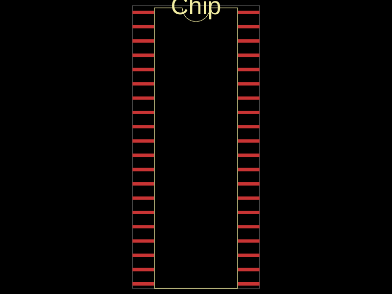
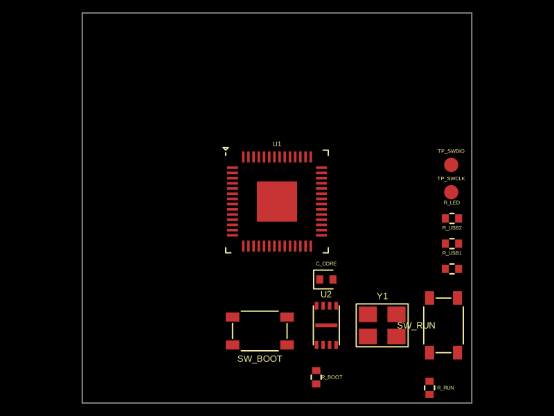
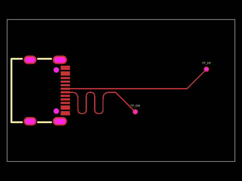
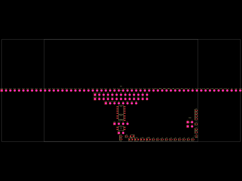
This circuit diagram depicts a Raspberry Pi Pico (RP2040) microcontroller with multiple GPIO, power regulation, crystal oscillator, external flash memory, USB interface, and peripheral connections including LEDs, push buttons, connectors, and optional NeoPixel, integrated on a custom PCB.
- Version
- 1.0.0
- License
- unset
- Stars
- 0
index.circuit.tsx
PCB
Schematic

const rp2040PinLabels = {
  pin1: "IOVDD",
  pin2: "GPIO0",
  pin3: "GPIO1",
  pin4: "GPIO2",
  pin5: "GPIO3",
  pin6: "GPIO4",
  pin7: "GPIO5",
  pin8: "GPIO6",
  pin9: "GPIO7",
  pin10: "IOVDD",
  pin11: "GPIO8",
  pin12: "GPIO9",
  pin13: "GPIO10",
  pin14: "GPIO11",
  pin15: "GPIO12",
  pin16: "GPIO13",
  pin17: "GPIO14",
  pin18: "GPIO15",
  pin19: "TESTEN",
  pin20: "XIN",
  pin21: "XOUT",
  pin22: "IOVDD",
  pin23: "DVDD",
  pin24: "SWCLK",
  pin25: "SWDIO",
  pin26: "RUN",
  pin27: "GPIO16",
  pin28: "GPIO17",
  pin29: "GPIO18",
  pin30: "GPIO19",
  pin31: "GPIO20",
  pin32: "GPIO21",
  pin33: "GPIO22",
  pin34: "GPIO23",
  pin35: "GPIO24",
  pin36: "GPIO25",
  pin37: "GPIO26_ADC0",
  pin38: "GPIO27_ADC1",
  pin39: "GPIO28_ADC2",
  pin40: "GPIO29_ADC3",
  pin41: "ADC_AVDD",
  pin42: "VREG_VIN",
  pin43: "VREG_VOUT",
  pin44: "USB_VDD",
  pin45: "GND",
  pin46: "USB_DM",
  pin47: "USB_DP",
  pin48: "QSPI_SD3",
  pin49: "QSPI_SCLK",
  pin50: "QSPI_SD0",
  pin51: "QSPI_SD2",
  pin52: "QSPI_SD1",
  pin53: "QSPI_SS",
  pin54: "GND",
  pin55: "DVDD",
  pin56: "IOVDD",
} as const

const decouplingCaps = [
  ["C8", "3V3", -13.2, -8.7],
  ["C9", "1V2", -11.9, -8.7],
  ["C10", "1V2", -10.6, -8.7],
  ["C11", "1V2", -9.3, -8.7],
  ["C12", "3V3", -8.0, -8.7],
  ["C13", "3V3", -6.7, -8.7],
  ["C14", "3V3", -5.4, -8.7],
  ["C15", "3V3", -4.1, -8.7],
  ["C16", "3V3", -2.8, -8.7],
  ["C17", "3V3", -1.5, -8.7],
] as const

const leftHeaderPins = [
  "D_PLUS",
  "D_MINUS",
  "D0",
  "GND",
  "D1",
  "D2",
  "D3",
  "D4",
  "D5",
  "D6",
  "D7",
  "D8",
  "D9",
] as const

const rightHeaderPins = [
  "D_MINUS",
  "RAW",
  "GND",
  "RESET",
  "V3V3",
  "A3",
  "A2",
  "A1",
  "A0",
  "SCLK",
  "MISO",
  "MOSI",
  "D10",
] as const

export default () => (
  <board width="90mm" height="60mm" routingDisabled>
    <schematicrect
      schX={-9}
      schY={-0.7}
      width={22}
      height={18}
      color="#e63946"
      strokeWidth={0.03}
      isDashed
    />
    <schematictext
      schX={-9}
      schY={8.1}
      text="RP2040 CORE"
      color="#e63946"
      fontSize={0.55}
    />
    <chip
      name="IC2"
      manufacturerPartNumber="RP2040"
      footprint="pinrow56"
      schX={-8.8}
      schY={-0.8}
      schWidth={8.8}
      schHeight={14}
      schPinSpacing={0.38}
      pinLabels={rp2040PinLabels}
      schPinArrangement={{
        leftSide: {
          pins: [
            "pin26",
            "pin1",
            "pin22",
            "pin41",
            "pin23",
            "pin43",
            "pin19",
            "pin20",
            "pin21",
            "pin36",
            "pin37",
            "pin38",
            "pin39",
            "pin40",
            "pin49",
            "pin53",
            "pin50",
            "pin52",
            "pin51",
            "pin48",
            "pin45",
          ],
          direction: "top-to-bottom",
        },
        rightSide: {
          pins: [
            "pin2",
            "pin3",
            "pin4",
            "pin5",
            "pin6",
            "pin7",
            "pin8",
            "pin9",
            "pin11",
            "pin12",
            "pin13",
            "pin14",
            "pin15",
            "pin16",
            "pin17",
            "pin18",
            "pin27",
            "pin28",
            "pin29",
            "pin30",
            "pin31",
            "pin32",
            "pin33",
            "pin34",
            "pin35",
            "pin46",
            "pin47",
            "pin24",
            "pin25",
          ],
          direction: "top-to-bottom",
        },
      }}
      connections={{
        IOVDD: "net.V3V3",
        GPIO0: "net.D0",
        GPIO1: "net.D1",
        GPIO2: "net.D2",
        GPIO3: "net.D3",
        GPIO4: "net.D4",
        GPIO5: "net.D5",
        GPIO6: "net.D6",
        GPIO7: "net.D7",
        GPIO8: "net.D8",
        GPIO9: "net.D9",
        GPIO10: "net.D10",
        GPIO11: "net.USBOOT",
        GPIO12: "net.SDA",
        GPIO13: "net.SCL",
        GPIO16: "net.NEOPIX",
        GPIO18: "net.SCLK",
        GPIO20: "net.MOSI",
        GPIO19: "net.MISO",
        GPIO26_ADC0: "net.A0",
        GPIO27_ADC1: "net.A1",
        GPIO28_ADC2: "net.A2",
        GPIO29_ADC3: "net.A3",
        RUN: "net.RESET",
        USB_DM: "net.D_MINUS",
        USB_DP: "net.D_PLUS",
        QSPI_SCLK: "net.QSPI_SCK",
        QSPI_SS: "net.QSPI_CS",
        QSPI_SD0: "net.QSPI_DATA0",
        QSPI_SD1: "net.QSPI_DATA1",
        QSPI_SD2: "net.QSPI_DATA2",
        QSPI_SD3: "net.QSPI_DATA3",
        VREG_VIN: "net.V3V3",
        USB_VDD: "net.V3V3",
        DVDD: "net.V1V2",
        ADC_AVDD: "net.V3V3",
        GND: "net.GND",
        TESTEN: "net.GND",
        XIN: "net.XIN",
        XOUT: "net.XOUT",
        SWCLK: "net.SWCLK",
        SWDIO: "net.SWDIO",
      }}
    />

    <crystal
      name="Y1"
      frequency="12MHz"
      loadCapacitance="10pF"
      footprint="pinrow2"
      schX={-14.2}
      schY={-1.2}
      schOrientation="vertical"
      connections={{ left: "net.XIN", right: "net.XOUT" }}
    />
    <capacitor
      name="C19"
      capacitance="22pF"
      footprint="0402"
      schX={-15.3}
      schY={-2.5}
      schOrientation="vertical"
      connections={{ pin1: "net.XIN", pin2: "net.GND" }}
    />
    <capacitor
      name="C20"
      capacitance="22pF"
      footprint="0402"
      schX={-14.0}
      schY={-2.5}
      schOrientation="vertical"
      connections={{ pin1: "net.XOUT", pin2: "net.GND" }}
    />
    <resistor
      name="R3"
      resistance="10k"
      footprint="0402"
      schX={-15.4}
      schY={2.2}
      schRotation={90}
      connections={{ pin1: "net.V3V3", pin2: "net.RESET" }}
    />
    <netlabel net="RESET" connectsTo=".IC2 > .RUN" schX={-14.0} schY={1.5} />
    <netlabel net="A0" connectsTo=".IC2 > .GPIO26_ADC0" schX={-15.9} schY={-5.1} />
    <netlabel net="A1" connectsTo=".IC2 > .GPIO27_ADC1" schX={-15.9} schY={-5.7} />
    <netlabel net="A2" connectsTo=".IC2 > .GPIO28_ADC2" schX={-15.9} schY={-6.3} />
    <netlabel net="A3" connectsTo=".IC2 > .GPIO29_ADC3" schX={-15.9} schY={-6.9} />

    <schematicrect
      schX={-4.8}
      schY={7.9}
      width={15.8}
      height={5.2}
      color="#e63946"
      strokeWidth={0.03}
      isDashed
    />
    <schematictext
      schX={-4.8}
      schY={10.3}
      text="POWER AND FILTERING"
      color="#e63946"
      fontSize={0.5}
    />
    <diode
      name="DPROT"
      displayName="D1"
      variant="schottky"
      footprint="0603"
      schX={-12.4}
      schY={8.5}
      connections={{ anode: "net.VBUS", cathode: "net.RAW" }}
    />
    <fuse
      name="F1"
      currentRating="500mA"
      footprint="0603"
      schX={-13.5}
      schY={9.8}
      connections={{ pin1: "net.VBUS", pin2: ".DPROT > .anode" }}
    />
    <chip
      name="U2"
      manufacturerPartNumber="AP2112K-3.3"
      footprint="soic5"
      schX={-8.5}
      schY={8.3}
      schWidth={4}
      schHeight={2.4}
      pinLabels={{
        pin1: "IN",
        pin2: "GND",
        pin3: "EN",
        pin4: "NC",
        pin5: "OUT",
      }}
      schPinArrangement={{ leftSide: ["pin1", "pin2", "pin3"], rightSide: ["pin5", "pin4"] }}
      connections={{ IN: "net.RAW", EN: "net.RAW", OUT: "net.V3V3", GND: "net.GND" }}
      noConnect={["NC"]}
    />
    <capacitor
      name="C1"
      capacitance="10uF"
      footprint="0603"
      schX={-14.0}
      schY={6.5}
      schOrientation="vertical"
      connections={{ pin1: "net.RAW", pin2: "net.GND" }}
    />
    <capacitor
      name="C4"
      capacitance="10uF"
      footprint="0603"
      schX={-5.8}
      schY={7.0}
      schOrientation="vertical"
      connections={{ pin1: "net.V3V3", pin2: "net.GND" }}
    />
    <led
      name="DPWR"
      displayName="D2"
      color="green"
      footprint="0603"
      schX={-2.4}
      schY={8.5}
      connections={{ anode: "net.V3V3", cathode: "net.PWR_LED_K" }}
    />
    <resistor
      name="R1"
      resistance="10k"
      footprint="0402"
      schX={-2.4}
      schY={7.0}
      connections={{ pin1: "net.PWR_LED_K", pin2: "net.GND" }}
    />
    {decouplingCaps.map(([name, rail, schX, schY]) => (
      <capacitor
        key={name}
        name={name}
        capacitance="0.1uF"
        footprint="0402"
        schX={schX}
        schY={schY}
        schOrientation="vertical"
        connections={{ pin1: rail === "3V3" ? "net.V3V3" : "net.V1V2", pin2: "net.GND" }}
      />
    ))}
    <capacitor
      name="C18"
      capacitance="1uF"
      footprint="0402"
      schX={0}
      schY={-8.7}
      schOrientation="vertical"
      connections={{ pin1: "net.V3V3", pin2: "net.GND" }}
    />

    <schematicrect
      schX={3.9}
      schY={7.8}
      width={9.8}
      height={5.4}
      color="#e63946"
      strokeWidth={0.03}
      isDashed
    />
    <schematictext schX={1.0} schY={10.3} text="RESET" color="#e63946" fontSize={0.5} />
    <schematictext schX={4.3} schY={10.3} text="QSPI_CS" color="#e63946" fontSize={0.5} />
    <resistor
      name="R2"
      resistance="10k"
      footprint="0402"
      schX={1.0}
      schY={8.6}
      connections={{ pin1: "net.V3V3", pin2: "net.USBOOT" }}
    />
    <pushbutton
      name="SW3"
      footprint="pinrow2"
      pinLabels={{ pin1: "A", pin2: "B" }}
      schX={1.0}
      schY={7.0}
      schWidth={2}
      schHeight={1.2}
      connections={{ A: "net.USBOOT", B: "net.GND" }}
    />
    <pushbutton
      name="SW2"
      footprint="pinrow2"
      pinLabels={{ pin1: "A", pin2: "B" }}
      schX={5.1}
      schY={7.0}
      schWidth={2}
      schHeight={1.2}
      connections={{ A: "net.RESET", B: "net.GND" }}
    />
    <resistor
      name="R7"
      resistance="1k"
      footprint="0402"
      schX={4.3}
      schY={8.6}
      connections={{ pin1: "net.V3V3", pin2: "net.QSPI_CS" }}
    />

    <schematicrect
      schX={10.9}
      schY={6.1}
      width={14.6}
      height={8.8}
      color="#e63946"
      strokeWidth={0.03}
      isDashed
    />
    <connector
      name="U3"
      standard="usb_c"
      footprint="pinrow8"
      schX={8.1}
      schY={8.4}
      schWidth={4.4}
      schHeight={4.8}
      pinLabels={{
        pin1: "VBUS",
        pin2: "D_PLUS",
        pin3: "D_MINUS",
        pin4: "CC1",
        pin5: "CC2",
        pin6: "SBU1",
        pin7: "SBU2",
        pin8: "GND",
      }}
      schPinArrangement={{
        rightSide: ["pin1", "pin2", "pin3", "pin4", "pin5", "pin6", "pin7", "pin8"],
      }}
      connections={{
        VBUS: "net.VBUS",
        D_PLUS: "net.D_PLUS",
        D_MINUS: "net.D_MINUS",
        CC1: "net.CC1",
        CC2: "net.CC2",
        GND: "net.GND",
      }}
      noConnect={["SBU1", "SBU2"]}
    />
    <resistor
      name="R8"
      resistance="5.1k"
      footprint="0402"
      schX={11.0}
      schY={6.4}
      connections={{ pin1: "net.CC1", pin2: "net.GND" }}
    />
    <resistor
      name="R9"
      resistance="5.1k"
      footprint="0402"
      schX={12.3}
      schY={6.9}
      connections={{ pin1: "net.CC2", pin2: "net.GND" }}
    />
    <netlabel net="VBUS" connectsTo=".U3 > .VBUS" schX={13.8} schY={9.5} />

    <pinheader
      name="CONN1"
      pinCount={4}
      gender="female"
      footprint="pinrow4"
      pinLabels={["GND", "V_PLUS", "SDA", "SCL"]}
      schX={7.4}
      schY={3.4}
      schFacingDirection="left"
      connections={{ GND: "net.GND", V_PLUS: "net.V3V3", SDA: "net.SDA", SCL: "net.SCL" }}
    />
    <schematictext
      schX={8.2}
      schY={2.0}
      text="STEMMA_I2C_QTSKINNY"
      color="#888888"
      fontSize={0.35}
    />
    <resistor
      name="R10"
      resistance="10k"
      footprint="0402"
      schX={5.0}
      schY={3.6}
      connections={{ pin1: "net.V3V3", pin2: "net.SDA" }}
    />
    <resistor
      name="R11"
      resistance="5.1k"
      footprint="0402"
      schX={5.0}
      schY={2.8}
      connections={{ pin1: "net.V3V3", pin2: "net.SCL" }}
    />

    <chip
      name="U5"
      manufacturerPartNumber="8MB QSPI Flash"
      footprint="soic8"
      schX={19.0}
      schY={8.0}
      schWidth={4.2}
      schHeight={3.6}
      pinLabels={{
        pin1: "SCK",
        pin2: "MOSI",
        pin3: "MISO",
        pin4: "SSEL",
        pin5: "WP_IO2",
        pin6: "HOLD_IO3",
        pin7: "VSS",
        pin8: "VCC",
      }}
      schPinArrangement={{
        leftSide: ["pin1", "pin2", "pin3", "pin4", "pin5", "pin6"],
        rightSide: ["pin8", "pin7"],
      }}
      connections={{
        SCK: "net.QSPI_SCK",
        MOSI: "net.QSPI_DATA0",
        MISO: "net.QSPI_DATA1",
        SSEL: "net.QSPI_CS",
        WP_IO2: "net.QSPI_DATA2",
        HOLD_IO3: "net.QSPI_DATA3",
        VSS: "net.GND",
        VCC: "net.V3V3",
      }}
    />
    <netlabel net="QSPI_SCK" connectsTo=".U5 > .SCK" schX={14.8} schY={9.4} />
    <netlabel net="QSPI_DATA0" connectsTo=".U5 > .MOSI" schX={14.8} schY={8.8} />
    <netlabel net="QSPI_DATA1" connectsTo=".U5 > .MISO" schX={14.8} schY={8.2} />
    <netlabel net="QSPI_CS" connectsTo=".U5 > .SSEL" schX={14.8} schY={7.6} />
    <netlabel net="QSPI_DATA2" connectsTo=".U5 > .WP_IO2" schX={14.8} schY={7.0} />
    <netlabel net="QSPI_DATA3" connectsTo=".U5 > .HOLD_IO3" schX={14.8} schY={6.4} />

    <chip
      name="NEO1"
      displayName="D3"
      manufacturerPartNumber="WS2812B"
      footprint="soic4"
      schX={18.0}
      schY={3.0}
      schWidth={3}
      schHeight={2.4}
      pinLabels={{ pin1: "VDD", pin2: "DIN", pin3: "DOUT", pin4: "GND" }}
      schPinArrangement={{ leftSide: ["pin2"], rightSide: ["pin3"], topSide: ["pin1"], bottomSide: ["pin4"] }}
      connections={{ VDD: "net.V3V3", DIN: "net.NEOPIX", GND: "net.GND" }}
      noConnect={["DOUT"]}
    />
    <netlabel net="NEOPIX" connectsTo=".NEO1 > .DIN" schX={15.0} schY={3.0} />

    <schematicrect
      schX={14.2}
      schY={-4.2}
      width={16.6}
      height={7.2}
      color="#e63946"
      strokeWidth={0.03}
      isDashed
    />
    <pinheader
      name="JP2"
      pinCount={13}
      gender="female"
      footprint="pinrow13"
      pinLabels={[...leftHeaderPins]}
      schX={10.0}
      schY={-4.2}
      schFacingDirection="right"
      schPinSpacing={0.45}
      connections={Object.fromEntries(
        leftHeaderPins.map((pin) => [pin, `net.${pin}`]),
      )}
    />
    <pinheader
      name="JP1"
      pinCount={13}
      gender="female"
      footprint="pinrow13"
      pinLabels={[...rightHeaderPins]}
      schX={18.6}
      schY={-4.2}
      schFacingDirection="left"
      schPinSpacing={0.45}
      connections={Object.fromEntries(
        rightHeaderPins.map((pin) => [
          pin,
          pin === "RAW" ? "net.RAW" : `net.${pin}`,
        ]),
      )}
    />

    <schematicrect
      schX={13.2}
      schY={-10.0}
      width={19.6}
      height={4.9}
      color="#e63946"
      strokeWidth={0.04}
    />
    <schematictext
      schX={9.3}
      schY={-8.8}
      text="ADAFRUIT INDUSTRIES"
      color="#e63946"
      fontSize={0.7}
    />
    <schematictext
      schX={9.3}
      schY={-10.0}
      text="Keeb 2040 rev B - tscircuit recreation"
      color="#e63946"
      fontSize={0.46}
    />
    <schematictext
      schX={16.8}
      schY={-11.3}
      text="FILE: index.circuit.tsx   PAGE: 1/1"
      color="#e63946"
      fontSize={0.4}
    />
  </board>
)