seveibar/pd-dual-stepper-controller
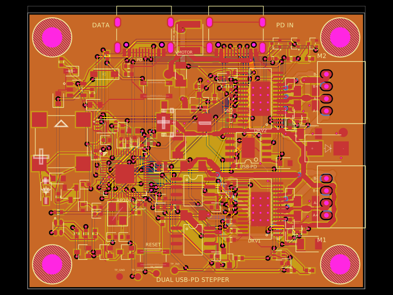
Bottom-side PCB silkscreen artwork consisting of embedded mirrored TS Circuit SVG logos, with via-clearance-aware lower-board placement.
- Version
- 0.1.0
- License
- unset
- Stars
- 0
index.circuit.tsx
PCB
Schematic

import { Fragment } from "react";
import * as Motor2 from "./schematic/Motor2DriverCoreSection";
import { Motor2OutputConnector, Motor2OutputTraces } from "./schematic/Motor2OutputsSection";
import { autoLayoutSections } from "./schematic/AutoLayoutSections";
import { PdVoltageControlSection } from "./schematic/PdVoltageControlSection";
import jlcClearanceRules from "./engineering/jlcpcb-clearance-rules.json";
import { ChipDescriptions } from "./schematic/ChipDescriptions";
import { tscircuitBottomLogo } from "./assets/tscircuit-logo-bottom";
import { Drv8825ThermalCopper } from "./schematic/Drv8825ThermalCopper";
import { CurrentTelemetrySection } from "./schematic/CurrentTelemetrySection";
import { StatusLedSection } from "./schematic/StatusLedSection";
import { ProductionTestPoints } from "./schematic/ProductionTestPoints";
import { FeedbackSection } from "./schematic/FeedbackSection";
import boardOutline from "./mechanical/dual-outline.json";
import { dualSavedRouting } from "./routing/dual-saved-routing";
import { ControllerSections } from "./schematic/ControllerSections";
import {
	MotorDriverController,
	MotorDriverControlTraces,
	MotorDriverGroundTraces,
	MotorDriverPassives,
	MotorDriverPowerTraces,
	MotorDriverPrimaryGroundTraces,
	MotorDriverSenseAndControlTraces,
} from "./schematic/MotorDriverCoreSection";
import {
	MotorOutputConnectors,
	MotorOutputTraces,
} from "./schematic/MotorOutputsSection";
import {
	MotorPowerFilteringComponents,
	MotorPowerFilteringGroundTrace,
	MotorPowerFilteringSupplyTrace,
} from "./schematic/MotorPowerFilteringSection";
import {
	MotorPowerPdConnectorGroundTraces,
	MotorPowerPdControllers,
	MotorPowerPdInputTraces,
	MotorPowerPdPassives,
	MotorPowerPdPrimaryGroundTrace,
	MotorPowerPdProtocolTraces,
	MotorPowerPdSupportGroundTraces,
} from "./schematic/MotorPowerPdNegotiationSection";
import { SchematicSheets } from "./schematic/SchematicSheets";
import { ThermalProtectionComponents, ThermalProtectionTraces } from "./schematic/ThermalProtectionSection";

/** The saved routing is guarded against changes to geometry and connectivity. */
export default function DualUsbPdStepperController({
	routingDisabled = false,
  routingAlgorithm = dualSavedRouting,
  finalizeGroundPours = false,
}: {
	routingDisabled?: boolean;
  routingAlgorithm?: typeof dualSavedRouting;
  finalizeGroundPours?: boolean;
} = {}) {
	// The DRV8825 footprint intentionally has thermal vias inside its exposed pad.
	// Core's placement check treats via-in-pad as a collision and skips routing.
	return autoLayoutSections(
    <board
      routingDisabled={routingDisabled}
			placementDrcChecksDisabled
			layers={4}
      thickness="1.6mm"
			outline={boardOutline}
			minViaHoleDiameter="0.2mm"
      minViaPadDiameter="0.45mm"
      minViaHoleEdgeToViaHoleEdgeClearance="0.2mm"
      minPlatedHoleDrillEdgeToDrillEdgeClearance="0.45mm"
      minViaEdgeToPadEdgeClearance="0.125mm"
      minTraceWidth={jlcClearanceRules.minimumMm.traceWidth}
      minTraceToPadEdgeClearance={jlcClearanceRules.minimumMm.padToTrace}
      // Native checks currently reuse this field for via-to-pad spacing.
      // checkJlcClearances separately enforces 0.15 mm between component pads.
      minPadEdgeToPadEdgeClearance={jlcClearanceRules.minimumMm.viaToPad}
      minBoardEdgeClearance={jlcClearanceRules.minimumMm.copperToBoardEdge}
			autorouterEffortLevel="2x"
			autorouterVersion="beta_pipeline7"
			autorouter={{
				local: true,
				...(routingAlgorithm ? {algorithmFn: routingAlgorithm} : {}),
				groupMode: "subcircuit",
			}}
		>
			<net name="GND" />
			{/* Explicit net names keep labels consistent across the MCU subcircuit and sheets. */}
			<net name="DRIVER_STEP" connectsTo=".MCU > .U1 > .GPIO18" />
			<net name="DRIVER_DIR" connectsTo=".MCU > .U1 > .GPIO19" />
			<net name="DRIVER_RESET" connectsTo=".MCU > .U1 > .GPIO20" />
			<net name="MCU_ENABLE" connectsTo=".MCU > .U1 > .GPIO22" />
			<net name="TEMP_SDA" connectsTo=".MCU > .U1 > .GPIO26_ADC0" />
			<net name="TEMP_SCL" connectsTo=".MCU > .U1 > .GPIO27_ADC1" />
			<SchematicSheets />
      <schematicsheet name="motor_2" displayName="Motor 2 — 1 A / 1/16 step" sheetIndex={11}>
        <schematicsection name="motor_2_core" displayName="Motor 2 DRV8825" />
        <schematicsection name="motor_2_outputs" displayName="Motor 2 Output" />
      </schematicsheet>

			<group pcbX={-5.625} pcbY={-8.25}>
				<ControllerSections />
				<MotorDriverController />
				<MotorPowerPdControllers />
				<MotorOutputConnectors />
				<MotorPowerFilteringComponents />
				<MotorPowerPdPassives />
				<MotorDriverPassives />
				<ThermalProtectionComponents />

				<MotorDriverControlTraces />
				<MotorPowerPdInputTraces />
				<MotorPowerFilteringSupplyTrace />
				<MotorPowerPdProtocolTraces />
				<MotorDriverPowerTraces />
				<MotorDriverPrimaryGroundTraces />
				<MotorPowerPdPrimaryGroundTrace />
				<MotorPowerPdConnectorGroundTraces />
				<MotorPowerFilteringGroundTrace />
				<MotorPowerPdSupportGroundTraces />
				<MotorDriverGroundTraces />
				<MotorOutputTraces />
				<MotorDriverSenseAndControlTraces />
				<ThermalProtectionTraces />
			</group>

			<copperpour
				name="GND_TOP"
				layer="top"
				connectsTo="net.GND"
				clearance="0.21mm"
				padMargin="0.2mm"
				traceMargin="0.2mm"
				boardEdgeMargin="0.3mm"
				coveredWithSolderMask
			/>
			<copperpour
				name="GND_BOTTOM"
				layer="bottom"
				connectsTo="net.GND"
				clearance="0.21mm"
				padMargin="0.2mm"
				traceMargin="0.2mm"
				boardEdgeMargin="0.3mm"
				coveredWithSolderMask
			/>

			<group pcbX={0} pcbY={0} schX={0} schY={0}>
        {[-21,26].flatMap((x,xi) => [-20,17].map((y,yi) => (
          <Fragment key={`${x}:${y}`}><keepout shape="circle" pcbX={x} pcbY={y} radius="3.2mm" layers={["top","bottom","inner1","inner2"]}/><hole name={`MH${xi*2+yi+1}`} pcbX={x} pcbY={y} diameter="3.3mm" /></Fragment>
        )))}
        {[-21,26].flatMap(x => [-20,17].map(y => (
          <Fragment key={`mount-${x}:${y}`}><silkscreencircle pcbX={x} pcbY={y} radius="3.2mm" strokeWidth="0.15mm" /></Fragment>
        )))}
        <silkscreentext text="DATA" pcbX={-13} pcbY={19} fontSize="1mm" />
        <silkscreentext text="PD IN" pcbX={17} pcbY={19} fontSize="1mm" />
        <silkscreentext text="DUAL USB-PD STEPPER" pcbX={2} pcbY={-22.5} fontSize="1mm" />

      </group>
			{/* Explicit source joins also give the MCU sheet the same net labels. */}
			<trace name="LABEL_STEP" from=".MCU > .U1 > .GPIO18" to="net.DRIVER_STEP" schDisplayLabel="DRIVER_STEP" />
			<trace name="LABEL_DIR" from=".MCU > .U1 > .GPIO19" to="net.DRIVER_DIR" schDisplayLabel="DRIVER_DIR" />
			<trace name="LABEL_RESET" from=".MCU > .U1 > .GPIO20" to="net.DRIVER_RESET" schDisplayLabel="DRIVER_RESET" />
			<trace name="LABEL_ENABLE" from=".MCU > .U1 > .GPIO22" to="net.MCU_ENABLE" schDisplayLabel="MCU_ENABLE" />
			<trace name="LABEL_TEMP_SDA" from=".MCU > .U1 > .GPIO26_ADC0" to="net.TEMP_SDA" schDisplayLabel="TEMP_SDA" />
			<trace name="LABEL_TEMP_SCL" from=".MCU > .U1 > .GPIO27_ADC1" to="net.TEMP_SCL" schDisplayLabel="TEMP_SCL" />
      <FeedbackSection />
      <CurrentTelemetrySection />
      <StatusLedSection />
      <ProductionTestPoints />

      <Drv8825ThermalCopper />
      <ChipDescriptions />
      <PdVoltageControlSection />
      <group pcbX={-5.625} pcbY={-8.25}>
        <Motor2.Motor2DriverController />
        <Motor2.Motor2DriverPassives />
        <Motor2.Motor2DriverControlTraces />
        <Motor2.Motor2DriverPowerTraces />
        <Motor2.Motor2DriverPrimaryGroundTraces />
        <Motor2.Motor2DriverGroundTraces />
        <Motor2.Motor2DriverSenseAndControlTraces />
        <Motor2OutputConnector />
        <Motor2OutputTraces />
      <resistor name="R_M2_REQUEST_PD" resistance="100k" footprint="0402" pcbX={32.625} pcbY={10.25}
        supplierPartNumbers={{jlcpcb:["C25741"]}} schSheetName="motor_2" schSectionName="motor_2_core"
        connections={{pin1:".Q_PD_ENABLE_M2 > .source",pin2:"net.GND"}} />
      </group>
      <silkscreentext text="RP2040" pcbX={-9} pcbY={-9.6} fontSize="0.75mm" />
      <silkscreentext text="DRV1" pcbX={12} pcbY={-16.2} fontSize="0.75mm" />
      <silkscreentext text="DRV2" pcbX={13} pcbY={1.8} fontSize="0.75mm" />
      <silkscreentext text="USB-PD" pcbX={11} pcbY={-4.1} fontSize="0.75mm" />
      <silkscreentext text="BOOT" pcbX={-4} pcbY={10.5} fontSize="0.75mm" />
      <silkscreentext text="RESET" pcbX={-4.5} pcbY={-16.8} fontSize="0.75mm" />
      <silkscreentext text="M1" pcbX={23} pcbY={-16} fontSize="1mm" />
      <silkscreentext text="M2" pcbX={23} pcbY={14} fontSize="1mm" />
      {[-9,8].flatMap(y => ["A+","A-","B+","B-"].map((label,i) =>
        <Fragment key={`${y}-${label}`}><silkscreentext text={label} pcbX={22} pcbY={y-3+i*2} fontSize="0.6mm" /></Fragment>
      ))}
		</board>
	);
}