seveibar/nrf52810
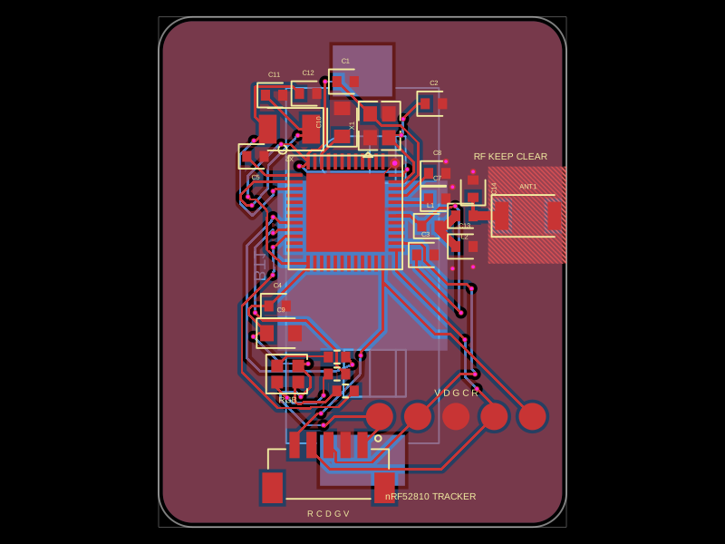
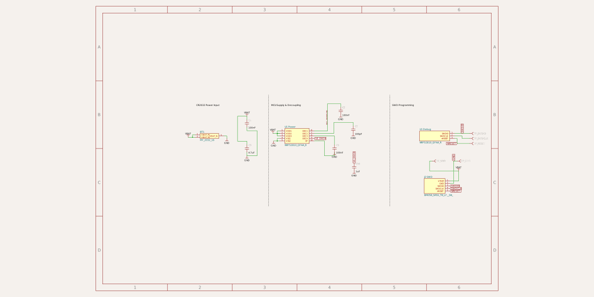
This code defines a PCB layout with key components including a 32.768kHz crystal oscillator, a microcontroller (nRF52810), LEDs, RF antenna, and supporting decoupling capacitors arranged on a multi-layer board.
- Version
- 0.1.3
- License
- unset
- Stars
- 0
index.circuit.tsx
PCB
Schematic
import { ABS07_32_768KHZ_9_T } from "./imports/ABS07_32_768KHZ_9_T";
import { BM05B_SRSS_TB_LF__SN_ } from "./imports/BM05B_SRSS_TB_LF__SN_";
import { E6C0606RGBC3UDA } from "./imports/E6C0606RGBC3UDA";
import { MY_2032_16 } from "./imports/MY_2032_16";
import { NRF52810_QFAA_R } from "./imports/NRF52810_QFAA_R";
import { RFANT3216120A5T } from "./imports/RFANT3216120A5T";
import { X201632MKB4SI } from "./imports/X201632MKB4SI";
const CORE_SHEET = "core-power";
const INTERFACE_SHEET = "status-led";
const CLOCK_SHEET = "clocks";
const RF_SHEET = "rf-front-end";
const CLOCK_SHEET_Y = 4;
const RF_SHEET_Y = -2;
const POWER_INPUT_SECTION = "power-input";
const MCU_POWER_SECTION = "mcu-power";
const PROGRAMMING_SECTION = "programming";
const STATUS_LED_SECTION = "status-led";
const HF_CLOCK_SECTION = "hf-clock";
const LF_CLOCK_SECTION = "lf-clock";
const RF_MATCH_SECTION = "rf-match";
const ANTENNA_SECTION = "antenna";
const HIDE_FOOTPRINT_TEXT = {
"& silkscreentext": { visibility: "hidden" as const },
};
const PcbCap = ({
name,
capacitance,
footprint = "0402",
pcbX,
pcbY,
pcbRotation,
schX,
schY,
schSectionName,
doNotPlace = false,
}: {
name: string;
capacitance: string;
footprint?: string;
pcbX: number;
pcbY: number;
pcbRotation?: number;
schX: number;
schY: number;
schSectionName: string;
doNotPlace?: boolean;
}) => (
<capacitor
name={name}
capacitance={capacitance}
footprint={footprint}
pcbX={pcbX}
pcbY={pcbY}
pcbRotation={pcbRotation}
schX={schX}
schY={schY}
schOrientation="vertical"
schSectionName={schSectionName}
doNotPlace={doNotPlace}
/>
);
export default () => (
<board
name="NRF52810_COINCELL_TRACKER"
title="nRF52810 CR2032 BLE Tracker"
width="24mm"
height="30mm"
outlineOffsetX={3}
borderRadius="2mm"
thickness="1.0mm"
layers={2}
solderMaskColor="black"
silkscreenColor="white"
doubleSidedAssembly
isViaInPadAllowed={false}
schLayout={{ layoutMode: "relative" }}
autorouter={{
preset: "auto_local",
allowViaInPad: false,
traceClearance: "0.15mm",
}}
>
{/* Drop top-side GND connections into the bottom ground plane first. */}
<autoroutingphase
name="GND_FANOUT"
phaseIndex={0}
connection="net.GND"
autorouter="fanout"
fanoutRoutingLayers={["top"]}
fanoutPourNetMap={{ bottom: "GND" }}
/>
<NRF52810_QFAA_R
name="U1"
pcbX={2.0}
pcbY={3.5}
noSchematicRepresentation
/>
<schematicsheet
name={CORE_SHEET}
displayName="Core, Power & Programming"
sheetIndex={0}
>
<schematicsection
name={POWER_INPUT_SECTION}
displayName="CR2032 Power Input"
/>
<schematicsection
name={MCU_POWER_SECTION}
displayName="MCU Supply & Decoupling"
/>
<schematicsection
name={PROGRAMMING_SECTION}
displayName="SWD Programming"
/>
<schematicbox
name="U1 Power"
chipRef=".U1"
width={1.96}
height={1.2}
schX={0}
schY={1}
schSectionName={MCU_POWER_SECTION}
pinLabels={{
pin1: "VDD1",
pin2: "VDD2",
pin3: "VDD3",
pin4: "VSS1",
pin5: "VSS2",
pin6: "DEC1",
pin7: "DEC2",
pin8: "DEC3",
pin9: "DEC4",
pin10: "EP",
}}
schPinArrangement={{
leftSide: ["pin1", "pin2", "pin3", "pin4", "pin5"],
rightSide: ["pin6", "pin7", "pin8", "pin9", "pin10"],
}}
/>
<schematicbox
name="U1 Debug"
chipRef=".U1"
width={2.4}
height={0.8}
schX={11}
schY={1}
schSectionName={PROGRAMMING_SECTION}
pinLabels={{
pin1: "SWDIO",
pin2: "SWDCLK",
pin3: "nRESET",
}}
schPinArrangement={{
leftSide: [],
rightSide: ["pin1", "pin2", "pin3"],
}}
/>
<BM05B_SRSS_TB_LF__SN_
name="J2"
pcbX={1}
pcbY={-11.5}
pcbSx={HIDE_FOOTPRINT_TEXT}
noSchematicRepresentation
/>
<schematicbox
name="J2 SWD"
chipRef=".J2"
width={1.67}
height={1.2}
schX={11}
schY={-3}
schSectionName={PROGRAMMING_SECTION}
pinLabels={{
pin1: "VTREF",
pin2: "GND",
pin3: "SWDIO",
pin4: "SWDCLK",
pin5: "nRESET",
}}
schPinArrangement={{
leftSide: [],
rightSide: ["pin1", "pin2", "pin3", "pin4", "pin5"],
}}
/>
<MY_2032_16
name="BT1"
layer="bottom"
pcbX={3}
pcbY={0.375}
pcbRotation={90}
schX={-7}
schY={1}
schHeight={0.4}
schSectionName={POWER_INPUT_SECTION}
schPinArrangement={{
leftSide: ["VBAT_P1", "VBAT_P2"],
rightSide: ["VBAT_N"],
}}
/>
<PcbCap
name="C4"
capacitance="100nF"
pcbX={-2}
pcbY={-2}
schX={-4}
schY={2}
schSectionName={POWER_INPUT_SECTION}
/>
<PcbCap
name="C9"
capacitance="4.7uF"
footprint="0603"
pcbX={-1.8}
pcbY={-3.6}
schX={-4}
schY={0}
schSectionName={POWER_INPUT_SECTION}
/>
<PcbCap
name="C5"
capacitance="100nF"
pcbX={-3.3}
pcbY={6.8}
schX={3.5}
schY={3}
schSectionName={MCU_POWER_SECTION}
/>
<PcbCap
name="C7"
capacitance="100pF"
pcbX={7.4}
pcbY={4.3}
schX={4.5}
schY={1.5}
schSectionName={MCU_POWER_SECTION}
/>
<PcbCap
name="C8"
capacitance="100nF"
pcbX={7.4}
pcbY={5.8}
schX={3}
schY={0}
schSectionName={MCU_POWER_SECTION}
/>
<PcbCap
name="C10"
capacitance="1uF"
footprint="0603"
pcbX={1.8}
pcbY={8.8}
pcbRotation={90}
schX={4.57}
schY={-1.5}
schSectionName={MCU_POWER_SECTION}
/>
<testpoint
name="TP_VDD"
footprintVariant="pad"
padShape="circle"
padDiameter="1.6mm"
pcbX={4}
pcbY={-8.5}
pcbSx={HIDE_FOOTPRINT_TEXT}
schX={11}
schY={-1}
schSectionName={PROGRAMMING_SECTION}
/>
<testpoint
name="TP_SWDIO"
footprintVariant="pad"
padShape="circle"
padDiameter="1.6mm"
pcbX={6.25}
pcbY={-8.5}
pcbSx={HIDE_FOOTPRINT_TEXT}
schX={14}
schY={1.2}
schSectionName={PROGRAMMING_SECTION}
/>
<testpoint
name="TP_GND"
footprintVariant="pad"
padShape="circle"
padDiameter="1.6mm"
pcbX={8.5}
pcbY={-8.5}
pcbSx={HIDE_FOOTPRINT_TEXT}
schX={13}
schY={-1}
schSectionName={PROGRAMMING_SECTION}
/>
<testpoint
name="TP_SWDCLK"
footprintVariant="pad"
padShape="circle"
padDiameter="1.6mm"
pcbX={10.75}
pcbY={-8.5}
pcbSx={HIDE_FOOTPRINT_TEXT}
schX={14}
schY={0.8}
schSectionName={PROGRAMMING_SECTION}
/>
<testpoint
name="TP_RESET"
footprintVariant="pad"
padShape="circle"
padDiameter="1.6mm"
pcbX={13}
pcbY={-8.5}
pcbSx={HIDE_FOOTPRINT_TEXT}
schX={14}
schY={0.4}
schSectionName={PROGRAMMING_SECTION}
/>
<trace from=".BT1 > .VBAT_P1" to="net.VBAT" width="0.15mm" />
<trace from=".BT1 > .VBAT_P2" to="net.VBAT" width="0.15mm" />
{/* BT1's bottom pad already sits directly in the bottom GND pour. */}
<trace
from=".BT1 > .VBAT_N"
to="net.GND"
width="0.15mm"
pcbPathRelativeTo=".BT1 > .VBAT_N"
pcbPath={[{ x: 0, y: 0.01 }]}
/>
<trace from=".U1 > .VDD1" to="net.VBAT" width="0.15mm" />
<trace from=".U1 > .VDD2" to="net.VBAT" width="0.15mm" />
<trace from=".U1 > .VDD3" to="net.VBAT" width="0.15mm" />
<trace from=".U1 > .VSS1" to="net.GND" width="0.15mm" />
<trace from=".U1 > .VSS2" to="net.GND" width="0.15mm" />
<trace
from=".U1 > .EP"
to="net.GND"
width="0.1mm"
pcbPathRelativeTo=".U1 > .EP"
pcbPath={[
{ x: 2.3, y: 2.3 },
{ x: 2.9, y: 2.9 },
]}
/>
<via
name="VIA_EP_GND"
pcbX={4.9}
pcbY={6.4}
holeDiameter="0.3mm"
outerDiameter="0.6mm"
connectsTo="net.GND"
/>
<trace from=".C4 > .pin1" to="net.VBAT" width="0.15mm" />
<trace from=".C4 > .pin2" to="net.GND" width="0.15mm" />
<trace from=".C9 > .pin1" to="net.VBAT" width="0.15mm" />
<trace from=".C9 > .pin2" to="net.GND" width="0.15mm" />
<trace
name="DEC1_DECOUPLING"
from=".U1 > .DEC1"
to=".C5 > .pin1"
width="0.15mm"
/>
<trace from=".C5 > .pin2" to="net.GND" width="0.15mm" />
<trace from=".U1 > .DEC2" to=".C7 > .pin1" width="0.15mm" />
<netlabel
net="GND"
connectsTo=".C7 > .pin2"
schX={4.5}
schY={1.2}
anchorSide="top"
/>
<trace from=".U1 > .DEC3" to=".C8 > .pin1" width="0.15mm" />
<netlabel
net="GND"
connectsTo=".C8 > .pin2"
schX={3}
schY={-0.3}
anchorSide="top"
/>
<via
name="VIA_C7_GND"
pcbX={8.3}
pcbY={5.0}
holeDiameter="0.2mm"
outerDiameter="0.35mm"
connectsTo={[".C7 > .pin2", "net.GND"]}
/>
<via
name="VIA_C8_GND"
pcbX={7.91}
pcbY={6.5}
holeDiameter="0.2mm"
outerDiameter="0.35mm"
connectsTo={[".C8 > .pin2", "net.GND"]}
/>
<trace from=".U1 > .DEC4" to=".C10 > .pin1" width="0.15mm" />
<trace from=".C10 > .pin2" to="net.GND" width="0.15mm" />
<trace from=".U1 > .SWDIO" to="net.SWDIO" width="0.15mm" />
<trace from=".TP_SWDIO > .pin1" to="net.SWDIO" width="0.15mm" />
<trace from=".U1 > .SWDCLK" to="net.SWDCLK" width="0.15mm" />
<trace from=".TP_SWDCLK > .pin1" to="net.SWDCLK" width="0.15mm" />
<trace from=".U1 > .nRESET" to="net.NRESET" width="0.15mm" />
<trace from=".TP_RESET > .pin1" to="net.NRESET" width="0.15mm" />
<trace from=".TP_VDD > .pin1" to="net.VBAT" width="0.15mm" />
<trace from=".TP_GND > .pin1" to="net.GND" width="0.15mm" />
<trace from=".J2 > .VTREF" to="net.VBAT" width="0.15mm" />
<trace from=".J2 > .GND" to="net.GND" width="0.15mm" />
<trace from=".J2 > .SWDIO" to="net.SWDIO" width="0.15mm" />
<trace from=".J2 > .SWDCLK" to="net.SWDCLK" width="0.15mm" />
<trace from=".J2 > .nRESET" to="net.NRESET" width="0.15mm" />
</schematicsheet>
<schematicsheet
name={INTERFACE_SHEET}
displayName="Status LED"
sheetIndex={1}
>
<schematicsection
name={STATUS_LED_SECTION}
displayName="RGB Status LED"
/>
<schematicbox
name="U1 Status GPIO"
chipRef=".U1"
width={2.2}
height={0.8}
schX={6.5}
schY={2}
schSectionName={STATUS_LED_SECTION}
pinLabels={{ pin1: "P0_06", pin2: "P0_07", pin3: "P0_08" }}
schPinArrangement={{
leftSide: [],
rightSide: ["pin1", "pin2", "pin3"],
}}
/>
<resistor
name="R_LED_B"
resistance="1k"
footprint="0402"
pcbX={1.5}
pcbY={-5}
pcbRotation={180}
pcbSx={HIDE_FOOTPRINT_TEXT}
schX={10}
schY={3.2}
schSectionName={STATUS_LED_SECTION}
/>
<resistor
name="R_LED_G"
resistance="1k"
footprint="0402"
pcbX={1.5}
pcbY={-6}
pcbRotation={180}
pcbSx={HIDE_FOOTPRINT_TEXT}
schX={10}
schY={2}
schSectionName={STATUS_LED_SECTION}
/>
<resistor
name="R_LED_R"
resistance="1k"
footprint="0402"
pcbX={2}
pcbY={-7}
pcbRotation={180}
pcbSx={HIDE_FOOTPRINT_TEXT}
schX={10}
schY={0.8}
schSectionName={STATUS_LED_SECTION}
/>
<E6C0606RGBC3UDA
name="LED1"
pcbX={-1.4}
pcbY={-6}
pcbSx={HIDE_FOOTPRINT_TEXT}
noSchematicRepresentation
/>
<schematicbox
name="LED1 RGB"
chipRef=".LED1"
width={2.2}
height={1}
schX={14}
schY={2}
schSectionName={STATUS_LED_SECTION}
pinLabels={{
pin1: "BLUE_K",
pin2: "GREEN_K",
pin3: "RED_K",
pin4: "COMMON_ANODE",
}}
schPinArrangement={{
leftSide: ["pin1", "pin2", "pin3", "pin4"],
rightSide: [],
}}
/>
<trace from=".U1 > .P0_06" to=".R_LED_B > .pin1" width="0.15mm" />
<trace from=".R_LED_B > .pin2" to=".LED1 > .BLUE_K" width="0.15mm" />
<trace from=".U1 > .P0_07" to=".R_LED_G > .pin1" width="0.15mm" />
<trace from=".R_LED_G > .pin2" to=".LED1 > .GREEN_K" width="0.15mm" />
<trace from=".U1 > .P0_08" to=".R_LED_R > .pin1" width="0.15mm" />
<trace from=".R_LED_R > .pin2" to=".LED1 > .RED_K" width="0.15mm" />
<trace from=".LED1 > .COMMON_ANODE" to="net.VBAT" width="0.15mm" />
</schematicsheet>
<schematicsheet
name={CLOCK_SHEET}
displayName="Clock Sources"
sheetIndex={2}
>
<schematicsection name={HF_CLOCK_SECTION} displayName="32 MHz Crystal" />
<schematicsection
name={LF_CLOCK_SECTION}
displayName="32.768 kHz Crystal"
/>
<schematicbox
name="U1 HF Clock"
chipRef=".U1"
width={2.4}
height={0.6}
schX={-7}
schY={CLOCK_SHEET_Y + 1}
schSectionName={HF_CLOCK_SECTION}
pinLabels={{ pin1: "XC1", pin2: "XC2" }}
schPinArrangement={{ leftSide: [], rightSide: ["pin1", "pin2"] }}
/>
<X201632MKB4SI
name="X1"
pcbX={4.0}
pcbY={8.6}
pcbRotation={90}
noSchematicRepresentation
/>
<schematicsymbol
name="X1_Symbol"
displayName="X1"
chipRef=".X1"
symbolName="crystal_4pin"
schX={-4}
schY={CLOCK_SHEET_Y + 1}
schSectionName={HF_CLOCK_SECTION}
connections={{
pin1: ".X1 > .XTAL1",
gnd1: ".X1 > .GND1",
pin3: ".X1 > .XTAL2",
gnd2: ".X1 > .GND2",
}}
/>
<PcbCap
name="C1"
capacitance="12pF"
pcbX={2.0}
pcbY={11.2}
schX={-5}
schY={CLOCK_SHEET_Y - 1}
schSectionName={HF_CLOCK_SECTION}
/>
<PcbCap
name="C2"
capacitance="12pF"
pcbX={7.2}
pcbY={9.9}
schX={-3}
schY={CLOCK_SHEET_Y - 1}
schSectionName={HF_CLOCK_SECTION}
/>
<schematicbox
name="U1 LF Clock"
chipRef=".U1"
width={2.4}
height={0.6}
schX={3}
schY={CLOCK_SHEET_Y + 1}
schSectionName={LF_CLOCK_SECTION}
pinLabels={{ pin1: "XL1", pin2: "XL2" }}
schPinArrangement={{ leftSide: [], rightSide: ["pin1", "pin2"] }}
/>
<ABS07_32_768KHZ_9_T
name="X2"
pcbX={-1.3}
pcbY={8.4}
pcbRotation={180}
noSchematicRepresentation
/>
<schematicsymbol
name="X2_Symbol"
displayName="X2"
chipRef=".X2"
symbolName="crystal"
schX={6}
schY={CLOCK_SHEET_Y + 1}
schSectionName={LF_CLOCK_SECTION}
connections={{
pin1: ".X2 > .OSC1",
pin2: ".X2 > .OSC2",
}}
/>
<PcbCap
name="C11"
capacitance="12pF"
pcbX={-2.2}
pcbY={10.4}
schX={5}
schY={CLOCK_SHEET_Y - 1}
schSectionName={LF_CLOCK_SECTION}
/>
<PcbCap
name="C12"
capacitance="12pF"
pcbX={-0.2}
pcbY={10.5}
schX={7}
schY={CLOCK_SHEET_Y - 1}
schSectionName={LF_CLOCK_SECTION}
/>
<trace
from=".U1 > .XC1"
to=".X1 > .XTAL1"
width="0.15mm"
maxLength="12mm"
schDisplayLabel="XC1"
/>
<trace
from=".U1 > .XC2"
to=".X1 > .XTAL2"
width="0.15mm"
maxLength="12mm"
schDisplayLabel="XC2"
/>
<trace from=".X1 > .GND1" to="net.GND" width="0.15mm" />
<trace from=".X1 > .GND2" to="net.GND" width="0.15mm" />
<trace
from=".X1 > .XTAL1"
to=".C1 > .pin1"
width="0.15mm"
schDisplayLabel="XC1"
/>
<trace from=".C1 > .pin2" to="net.GND" width="0.15mm" />
<trace
from=".X1 > .XTAL2"
to=".C2 > .pin1"
width="0.15mm"
schDisplayLabel="XC2"
/>
<trace from=".C2 > .pin2" to="net.GND" width="0.15mm" />
<trace
from=".U1 > .XL1"
to=".X2 > .OSC1"
width="0.15mm"
maxLength="12mm"
schDisplayLabel="XL1"
/>
<trace
from=".U1 > .XL2"
to=".X2 > .OSC2"
width="0.15mm"
maxLength="12mm"
schDisplayLabel="XL2"
/>
<trace
from=".X2 > .OSC1"
to=".C11 > .pin1"
width="0.15mm"
schDisplayLabel="XL1"
/>
<trace from=".C11 > .pin2" to="net.GND" width="0.15mm" />
<trace
from=".X2 > .OSC2"
to=".C12 > .pin1"
width="0.15mm"
schDisplayLabel="XL2"
/>
<trace from=".C12 > .pin2" to="net.GND" width="0.15mm" />
</schematicsheet>
<schematicsheet
name={RF_SHEET}
displayName="RF Front End & Antenna"
sheetIndex={3}
>
<schematicsection
name={RF_MATCH_SECTION}
displayName="Matching Network"
/>
<schematicsection name={ANTENNA_SECTION} displayName="Chip Antenna" />
<schematicbox
name="U1 RF"
chipRef=".U1"
width={2.2}
height={0.4}
schX={-6}
schY={RF_SHEET_Y + 1}
schSectionName={RF_MATCH_SECTION}
pinLabels={{ pin1: "ANT" }}
schPinArrangement={{ leftSide: [], rightSide: ["pin1"] }}
/>
<inductor
name="L1"
inductance="3.9nH"
footprint="0402"
pcbX={7}
pcbY={2.7}
schX={-3}
schY={RF_SHEET_Y + 1}
schSectionName={RF_MATCH_SECTION}
/>
<PcbCap
name="C3"
capacitance="0.8pF"
pcbX={6.7}
pcbY={1}
schX={-3}
schY={RF_SHEET_Y - 1}
schSectionName={RF_MATCH_SECTION}
/>
<inductor
name="L2"
inductance="6.8nH"
footprint="0402"
pcbX={9.0}
pcbY={3.3}
schX={0}
schY={RF_SHEET_Y + 1}
schSectionName={RF_MATCH_SECTION}
/>
<PcbCap
name="C13"
capacitance="0.5pF"
pcbX={9.0}
pcbY={1.5}
schX={-0.5}
schY={RF_SHEET_Y - 1}
schSectionName={RF_MATCH_SECTION}
doNotPlace
/>
<PcbCap
name="C14"
capacitance="0.5pF"
pcbX={9.51}
pcbY={4.9}
pcbRotation={90}
schX={2}
schY={RF_SHEET_Y - 1}
schSectionName={RF_MATCH_SECTION}
doNotPlace
/>
<RFANT3216120A5T
name="ANT1"
pcbX={12.75}
pcbY={3.3}
schX={6.82}
schY={RF_SHEET_Y + 1}
schSectionName={ANTENNA_SECTION}
/>
<trace
from=".U1 > .ANT"
to=".L1 > .pin1"
width="0.18mm"
maxLength="4mm"
pcbPathRelativeTo=".U1 > .ANT"
pcbPath={[
{ x: 3.8, y: -0.2 },
{ x: 4.49, y: -0.8 },
]}
/>
<trace
from=".L1 > .pin1"
to=".C3 > .pin1"
width="0.18mm"
maxLength="4mm"
/>
<trace
from=".C3 > .pin2"
to="net.GND"
width="0.15mm"
pcbPathRelativeTo=".C3 > .pin2"
pcbPath={[
{ x: 1.6, y: -0.8 },
{ x: 1.6, y: -0.8, via: true, toLayer: "bottom" },
{ x: 1.6, y: -0.8 },
]}
/>
<trace
from=".L1 > .pin2"
to=".L2 > .pin1"
width="0.5mm"
maxLength="5mm"
/>
<trace
from=".L1 > .pin2"
to=".C13 > .pin1"
width="0.18mm"
maxLength="8mm"
/>
<trace
from=".C13 > .pin2"
to="net.GND"
width="0.15mm"
pcbPathRelativeTo=".C13 > .pin2"
pcbPath={[
{ x: 0.51, y: -1.2 },
{ x: 0.51, y: -1.2, via: true, toLayer: "bottom" },
{ x: 0.51, y: -1.2 },
]}
/>
<trace
name="RF_FEED"
from=".L2 > .pin2"
to=".ANT1 > .FEED"
width="0.5mm"
maxLength="12mm"
pcbPathRelativeTo=".L2 > .pin2"
pcbPath={["ANT1.FEED"]}
/>
<trace
name="RF_SHUNT_C14"
from=".L2 > .pin2"
to=".C14 > .pin1"
width="0.18mm"
maxLength="2mm"
pcbPathRelativeTo=".L2 > .pin2"
pcbPath={["C14.pin1"]}
/>
<via
name="VIA_C14_GND"
pcbX={9.51}
pcbY={5.9}
holeDiameter="0.2mm"
outerDiameter="0.35mm"
connectsTo={[".C14 > .pin2", "net.GND"]}
/>
</schematicsheet>
<keepout
shape="rect"
pcbX={12.7}
pcbY={3.35}
width="4.6mm"
height="5.7mm"
layers={["top", "bottom"]}
excludeRefs={[".ANT1"]}
/>
<copperpour
name="TOP_GND"
layer="top"
connectsTo="net.GND"
clearance="0.2mm"
boardEdgeMargin="0.25mm"
/>
<copperpour
name="BOTTOM_GND"
layer="bottom"
connectsTo="net.GND"
clearance="0.2mm"
boardEdgeMargin="0.25mm"
/>
<silkscreentext
text="nRF52810 TRACKER"
pcbX={7}
pcbY={-13.2}
fontSize="0.55mm"
/>
<silkscreentext
text="RF KEEP CLEAR"
pcbX={11.7}
pcbY={6.8}
fontSize="0.55mm"
/>
<silkscreentext text="V D G C R" pcbX={8.5} pcbY={-7.1} fontSize="0.55mm" />
<silkscreentext text="R C D G V" pcbX={1} pcbY={-14.2} fontSize="0.5mm" />
<silkscreentext text="RGB" pcbX={-1.4} pcbY={-7.5} fontSize="0.5mm" />
</board>
);