seveibar/nrf-smart-watch
This code defines a detailed 3D PCB layout with schematic components, connectors, passive components, and RF antenna elements for a compact nRF52810-based smartwatch, including precise placement, copper pours, keepouts, and annotations.
- Version
- 0.1.1
- License
- unset
- Stars
- 0
index.circuit.tsx
PCB
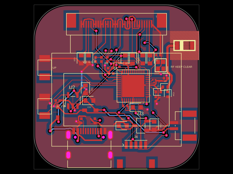
Schematic
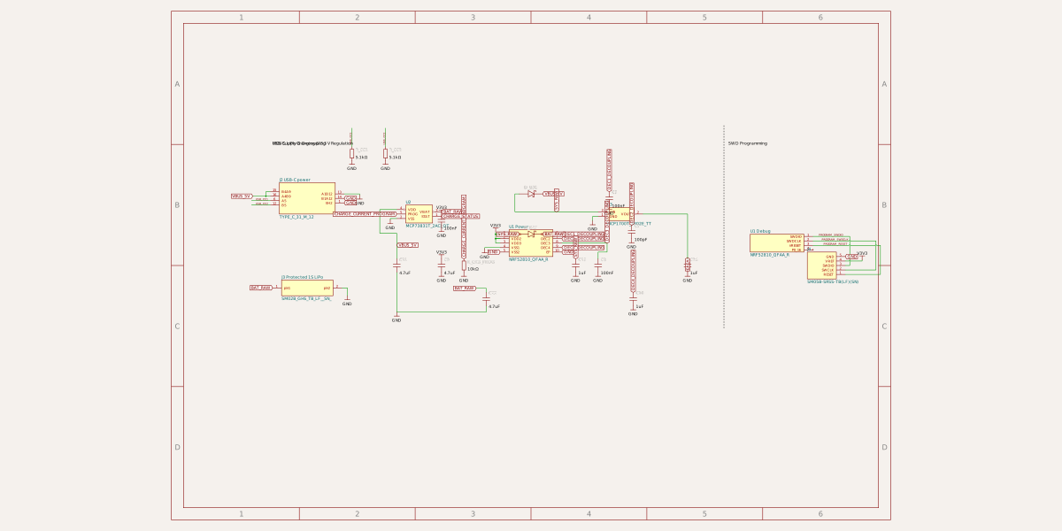
import { ER_CON30HT_1 } from "./imports/ER_CON30HT_1";
import { SM05B_SRSS_TB_LF__SN_ } from "./imports/SM05B_SRSS_TB_LF__SN_/SM05B_SRSS_TB_LF__SN_";
import { MCP1700T_3302E_TT } from "./imports/MCP1700T_3302E_TT";
import { MCP73831T_2ACI_OT } from "./imports/MCP73831T_2ACI_OT";
import { NRF52810_QFAA_R } from "./imports/NRF52810_QFAA_R";
import { RFANT3216120A5T } from "./imports/RFANT3216120A5T";
import { SM02B_GHS_TB_LF__SN_ } from "./imports/SM02B_GHS_TB_LF__SN_";
import { TYPE_C_31_M_12 } from "./imports/TYPE_C_31_M_12";
import { WATCH_SIDE_BUTTON } from "./imports/WATCH_SIDE_BUTTON";
import { X201632MKB4SI } from "./imports/X201632MKB4SI";
import type { FootprintProp } from "@tscircuit/props";
const CORE_SHEET = "core-power";
const INTERFACE_SHEET = "status-led";
const CLOCK_SHEET = "clocks";
const RF_SHEET = "rf-front-end";
const CLOCK_SHEET_Y = 4;
const RF_SHEET_Y = -2;
const POWER_INPUT_SECTION = "power-input";
const MCU_POWER_SECTION = "mcu-power";
const PROGRAMMING_SECTION = "programming";
const HF_CLOCK_SECTION = "hf-clock";
const RF_MATCH_SECTION = "rf-match";
const ANTENNA_SECTION = "antenna";
const DISPLAY_SECTION = "oled-display";
const CONTROLS_SECTION = "watch-controls";
const BOARD_SIZE = 34;
const BOARD_EDGE = BOARD_SIZE / 2;
const BOARD_RADIUS = 7;
const RF_ZONE_SIZE = 6;
const RF_ZONE_X = BOARD_EDGE - RF_ZONE_SIZE / 2;
const RF_ZONE_LEFT = BOARD_EDGE - RF_ZONE_SIZE;
// The centered OLED folds over the low-profile top-side assembly. Move the
// antenna above its metal-backed panel while leaving the matching network next
// to the MCU, outside the keepout.
const OLED_CONNECTOR_X = 0;
const OLED_CONNECTOR_Y = 13;
const OLED_PANEL_TOP_Y = OLED_CONNECTOR_Y - 6;
const OLED_SUPPORT_ROW_Y = OLED_PANEL_TOP_Y - 1.3;
const OLED_TO_RF_CLEARANCE = 0.75;
const ANTENNA_FOOTPRINT_HALF_HEIGHT = 0.83;
const RF_ZONE_Y =
OLED_PANEL_TOP_Y + OLED_TO_RF_CLEARANCE + ANTENNA_FOOTPRINT_HALF_HEIGHT;
const RF_MATCH_Y = 0;
const RF_MATCH_L2_X = RF_ZONE_LEFT - 0.95;
const RF_MATCH_L1_X = RF_MATCH_L2_X - 1.45;
const RF_MATCH_L1_Y = RF_MATCH_Y - 1;
const MCU_X = RF_MATCH_L2_X - 6.61;
const MCU_Y = RF_MATCH_Y + 0.2;
const HIDE_FOOTPRINT_TEXT = {
"& silkscreentext": { visibility: "hidden" as const },
};
const makeJlc0402CapFootprint = () => (
<footprint>
<smtpad
portHints={["pin2"]}
pcbX="0.420116mm"
pcbY={0}
width="0.499999mm"
height="0.540004mm"
shape="rect"
/>
<smtpad
portHints={["pin1"]}
pcbX="-0.420116mm"
pcbY={0}
width="0.499999mm"
height="0.540004mm"
shape="rect"
/>
<courtyardrect pcbX={0} pcbY={0} width="1.54mm" height="0.74mm" />
</footprint>
);
const makeJlc0201CapFootprint = () => (
<footprint>
<smtpad
portHints={["pin2"]}
pcbX="0.27432mm"
pcbY={0}
width="0.368427mm"
height="0.3240024mm"
shape="rect"
/>
<smtpad
portHints={["pin1"]}
pcbX="-0.27432mm"
pcbY={0}
width="0.368427mm"
height="0.3240024mm"
shape="rect"
/>
<courtyardrect pcbX={0} pcbY={0} width="1.12mm" height="0.54mm" />
</footprint>
);
const makeJlc0402ResFootprint = () => (
<footprint>
<smtpad
portHints={["pin2"]}
pcbX="0.432816mm"
pcbY={0}
width="0.565658mm"
height="0.540004mm"
shape="rect"
/>
<smtpad
portHints={["pin1"]}
pcbX="-0.432816mm"
pcbY={0}
width="0.565658mm"
height="0.540004mm"
shape="rect"
/>
<courtyardrect pcbX={0} pcbY={0} width="1.64mm" height="0.74mm" />
</footprint>
);
const makeC124205Footprint = () => (
<footprint>
<smtpad
portHints={["cathode"]}
pcbX="-1.172464mm"
pcbY={0}
width="0.999998mm"
height="0.6999986mm"
shape="rect"
/>
<smtpad
portHints={["anode"]}
pcbX="1.172464mm"
pcbY={0}
width="0.999998mm"
height="0.6999986mm"
shape="rect"
/>
<courtyardrect pcbX={0} pcbY={0} width="3.64mm" height="1.6mm" />
</footprint>
);
const PcbCap = ({
name,
capacitance,
footprint = "0402",
pcbX,
pcbY,
pcbRotation,
schX,
schY,
schOrientation = "vertical",
schSectionName,
doNotPlace = false,
layer,
maxDecouplingTraceLength,
manufacturerPartNumber,
supplierPartNumbers,
}: {
name: string;
capacitance: string;
footprint?: FootprintProp;
pcbX: number;
pcbY: number;
pcbRotation?: number;
schX: number;
schY: number;
schOrientation?: "horizontal" | "vertical";
schSectionName: string;
doNotPlace?: boolean;
layer?: "top" | "bottom";
maxDecouplingTraceLength?: string;
manufacturerPartNumber?: string;
supplierPartNumbers?: Record<string, string[]>;
}) => (
<capacitor
name={name}
capacitance={capacitance}
footprint={footprint}
pcbX={pcbX}
pcbY={pcbY}
pcbRotation={pcbRotation}
schX={schX}
schY={schY}
schOrientation={schOrientation}
schSectionName={schSectionName}
doNotPlace={doNotPlace}
layer={layer}
maxDecouplingTraceLength={maxDecouplingTraceLength}
manufacturerPartNumber={manufacturerPartNumber}
supplierPartNumbers={supplierPartNumbers}
/>
);
export default () => (
<board
name="NRF52810_SMART_WATCH"
title="nRF52810 OLED Smart Watch"
width={`${BOARD_SIZE}mm`}
height={`${BOARD_SIZE}mm`}
borderRadius={`${BOARD_RADIUS}mm`}
thickness="1.0mm"
layers={2}
allowBlindAndBuriedVias={false}
solderMaskColor="black"
silkscreenColor="white"
doubleSidedAssembly={false}
isViaInPadAllowed={false}
minViaHoleDiameter="0.3mm"
minViaPadDiameter="0.6mm"
minViaEdgeToPadEdgeClearance="0.1mm"
pcbStyle={{
viaHoleDiameter: "0.3mm",
viaPadDiameter: "0.6mm",
}}
minTraceToPadEdgeClearance="0.05mm"
schLayout={{ layoutMode: "relative" }}
autorouterVersion="beta_pipeline9"
autorouter={{
preset: "default",
allowViaInPad: false,
traceClearance: "0.1mm",
}}
>
<autoroutingphase name="RF shunt" phaseIndex={0} />
<autoroutingphase name="RF feed" phaseIndex={1} />
<autoroutingphase name="HF clock" phaseIndex={2} />
<autoroutingphase name="DEC1 decoupling" phaseIndex={3} />
<autoroutingphase name="Power decoupling" phaseIndex={4} />
<NRF52810_QFAA_R
name="U1"
pcbX={MCU_X}
pcbY={MCU_Y}
noSchematicRepresentation
/>
<schematicsheet
name={CORE_SHEET}
displayName="Core, Power & Programming"
sheetIndex={0}
>
<schematicsection
name={POWER_INPUT_SECTION}
displayName="USB-C, LiPo Charging & 3.3 V Regulation"
/>
<schematicsection
name={MCU_POWER_SECTION}
displayName="MCU Supply & Decoupling"
/>
<schematicsection
name={PROGRAMMING_SECTION}
displayName="SWD Programming"
/>
<schematicbox
name="U1 Power"
chipRef=".U1"
width={1.96}
height={1.2}
schX={0}
schY={1}
schSectionName={MCU_POWER_SECTION}
pinLabels={{
pin1: "VDD1",
pin2: "VDD2",
pin3: "VDD3",
pin4: "VSS1",
pin5: "VSS2",
pin6: "DEC1",
pin7: "DEC2",
pin8: "DEC3",
pin9: "DEC4",
pin10: "EP",
}}
schPinArrangement={{
leftSide: ["pin1", "pin2", "pin3", "pin4", "pin5"],
rightSide: ["pin6", "pin7", "pin8", "pin9", "pin10"],
}}
/>
<schematicbox
name="U1 Debug"
chipRef=".U1"
width={2.4}
height={0.8}
schX={11}
schY={1}
schSectionName={PROGRAMMING_SECTION}
pinLabels={{
pin1: "SWDIO",
pin2: "SWDCLK",
pin3: "nRESET",
pin4: "P0_16",
}}
schPinArrangement={{
leftSide: [],
rightSide: ["pin1", "pin2", "pin3", "pin4"],
}}
/>
<TYPE_C_31_M_12
name="J2"
pcbX={-5.6}
pcbY={-11.3}
pcbSx={HIDE_FOOTPRINT_TEXT}
noSchematicRepresentation
/>
<schematicbox
name="J2 USB-C power"
chipRef=".J2"
width={2.5}
height={1.4}
schX={-10}
schY={3}
schSectionName={POWER_INPUT_SECTION}
pinLabels={{
pin15: "B4A9",
pin16: "A4B9",
pin6: "A5",
pin12: "B5",
pin13: "A1B12",
pin14: "B1A12",
pin1: "EH2",
}}
schPinArrangement={{
leftSide: ["pin15", "pin16", "pin6", "pin12"],
rightSide: ["pin13", "pin14", "pin1"],
}}
/>
<SM02B_GHS_TB_LF__SN_
name="J3"
pcbX={13.75}
pcbY={-8}
pcbRotation={90}
pcbSx={HIDE_FOOTPRINT_TEXT}
noSchematicRepresentation
/>
<schematicbox
name="J3 Protected 1S LiPo"
chipRef=".J3"
width={2.3}
height={0.7}
schX={-10}
schY={-1}
schSectionName={POWER_INPUT_SECTION}
pinLabels={{ pin1: "pin1", pin2: "pin2" }}
schPinArrangement={{ leftSide: ["pin1"], rightSide: ["pin2"] }}
/>
<MCP73831T_2ACI_OT
name="U2"
pcbX={-9}
pcbY={-2.8}
schX={-5}
schY={2.3}
schSectionName={POWER_INPUT_SECTION}
schPinArrangement={{
leftSide: ["VDD", "PROG", "VSS"],
rightSide: ["VBAT", "STAT"],
}}
/>
<MCP1700T_3302E_TT
name="U3"
pcbX={5}
pcbY={-8}
schX={4}
schY={2.3}
schSectionName={POWER_INPUT_SECTION}
schPinArrangement={{ leftSide: ["VIN", "GND"], rightSide: ["VOUT"] }}
/>
<resistor
name="R_CC1"
resistance="5.1k"
footprint={makeJlc0402ResFootprint()}
pcbX={-7.25}
pcbY={-7}
pcbRotation={-90}
schX={-8}
schY={5}
schOrientation="vertical"
schSectionName={POWER_INPUT_SECTION}
/>
<resistor
name="R_CC2"
resistance="5.1k"
footprint={makeJlc0402ResFootprint()}
pcbX={-4.45}
pcbY={-7}
pcbRotation={-90}
schX={-6.5}
schY={5}
schOrientation="vertical"
schSectionName={POWER_INPUT_SECTION}
/>
<resistor
name="R_CHG_PROG"
resistance="10k"
footprint={makeJlc0402ResFootprint()}
pcbX={-12.1}
pcbY={-2.8}
schX={-3}
schY={0}
schOrientation="vertical"
schSectionName={POWER_INPUT_SECTION}
/>
<diode
name="D_USB"
schottky
footprint={makeC124205Footprint()}
supplierPartNumbers={{ jlcpcb: ["C124205"] }}
pcbX={-12.1}
pcbY={-5.2}
pcbRotation={270}
schX={0}
schY={3.2}
schSectionName={POWER_INPUT_SECTION}
/>
<diode
name="D_BAT"
schottky
footprint={makeC124205Footprint()}
supplierPartNumbers={{ jlcpcb: ["C124205"] }}
pcbX={-5.4}
pcbY={-4.8}
schX={0}
schY={1.4}
schSectionName={POWER_INPUT_SECTION}
/>
<PcbCap
name="C21"
capacitance="4.7uF"
footprint="0603"
pcbX={-6.4}
pcbY={-0.5}
pcbRotation={-90}
schX={-6}
schY={0}
schSectionName={POWER_INPUT_SECTION}
maxDecouplingTraceLength="5mm"
/>
<PcbCap
name="C22"
capacitance="4.7uF"
footprint="0603"
pcbX={-5.6}
pcbY={-2.8}
schX={-2}
schY={-1.5}
schSectionName={POWER_INPUT_SECTION}
maxDecouplingTraceLength="8mm"
/>
<PcbCap
name="C23"
capacitance="1uF"
footprint="0603"
pcbX={1.3}
pcbY={-8}
schX={2}
schY={0}
schSectionName={POWER_INPUT_SECTION}
maxDecouplingTraceLength="5mm"
/>
<PcbCap
name="C24"
capacitance="1uF"
footprint="0603"
pcbX={7.75}
pcbY={-8}
pcbRotation={-90}
schX={7}
schY={0}
schSectionName={POWER_INPUT_SECTION}
maxDecouplingTraceLength="6mm"
/>
<PcbCap
name="C4"
capacitance="100nF"
footprint={makeJlc0402CapFootprint()}
pcbX={1.8}
pcbY={-3.9}
schX={-4}
schY={2}
schSectionName={MCU_POWER_SECTION}
maxDecouplingTraceLength="3mm"
/>
{/* C9 is bulk rail storage; C4 carries the strict local VDD1 limit. */}
<PcbCap
name="C9"
capacitance="4.7uF"
footprint="0603"
pcbX={4.2}
pcbY={-4.2}
schX={-4}
schY={0}
schSectionName={MCU_POWER_SECTION}
/>
<PcbCap
name="C5"
capacitance="100nF"
footprint={makeJlc0402CapFootprint()}
pcbX={-1.1}
pcbY={2.8}
pcbRotation={180}
schX={3.5}
schY={3}
schSectionName={MCU_POWER_SECTION}
/>
<PcbCap
name="C7"
capacitance="100pF"
footprint={makeJlc0201CapFootprint()}
pcbX={MCU_X + 4.31}
pcbY={MCU_Y + 0.45}
pcbRotation={270}
schX={4.5}
schY={1.5}
schSectionName={MCU_POWER_SECTION}
manufacturerPartNumber="GRM0335C1H101FA01D"
supplierPartNumbers={{ jlcpcb: ["C384957"] }}
/>
<PcbCap
name="C8"
capacitance="100nF"
footprint={makeJlc0201CapFootprint()}
pcbX={MCU_X + 4.31}
pcbY={MCU_Y + 1.3}
schX={3}
schY={0}
schSectionName={MCU_POWER_SECTION}
manufacturerPartNumber="TCC0201X5R104K100ZT"
supplierPartNumbers={{ jlcpcb: ["C5142565"] }}
/>
<PcbCap
name="C10"
capacitance="1uF"
footprint={makeJlc0402CapFootprint()}
pcbX={0.6}
pcbY={4.6}
pcbRotation={90}
schX={4.57}
schY={-1.5}
schSectionName={MCU_POWER_SECTION}
/>
<SM05B_SRSS_TB_LF__SN_
name="J4"
pcbX={4}
pcbY={-12}
schX={13}
schY={0}
schSectionName={PROGRAMMING_SECTION}
/>
<trace
name="USB_VBUS_PIN_BRIDGE"
from=".J2 > .A4B9"
to=".J2 > .B4A9"
width="0.3mm"
schDisplayLabel="VBUS_5V"
/>
<trace
name="USB_VBUS_TO_D_USB"
from=".J2 > .B4A9"
to=".D_USB > .anode"
width="0.3mm"
schDisplayLabel="VBUS_5V"
/>
<trace from=".J2 > .A1B12" to="net.GND" width="0.15mm" />
<trace from=".J2 > .B1A12" to="net.GND" width="0.15mm" />
<trace from=".J2 > .EH1" to="net.GND" width="0.15mm" />
<trace from=".J2 > .EH2" to="net.GND" width="0.15mm" />
<trace from=".J2 > .EH3" to="net.GND" width="0.15mm" />
<trace from=".J2 > .EH4" to="net.GND" width="0.15mm" />
<trace
name="USB_CC1"
from=".J2 > .A5"
to=".R_CC1 > .pin1"
width="0.1mm"
/>
<trace from=".R_CC1 > .pin2" to="net.GND" width="0.15mm" />
<trace
name="USB_CC2"
from=".J2 > .B5"
to=".R_CC2 > .pin1"
width="0.1mm"
/>
<trace from=".R_CC2 > .pin2" to="net.GND" width="0.15mm" />
<trace
name="USB_TO_CHARGER_VDD"
from=".D_USB > .anode"
to=".U2 > .VDD"
width="0.3mm"
schDisplayLabel="VBUS_5V"
/>
<trace from=".U2 > .VSS" to="net.GND" width="0.15mm" />
<trace
name="CHARGER_VDD_DECOUPLING"
from=".U2 > .VDD"
to=".C21 > .pin1"
width="0.3mm"
routingPhaseIndex={4}
/>
<trace
name="CHARGER_VDD_LOCAL_GROUND"
from=".C21 > .pin2"
to=".U2 > .VSS"
width="0.15mm"
routingPhaseIndex={4}
/>
<trace
name="CHARGE_CURRENT_PROGRAM"
from=".U2 > .PROG"
to=".R_CHG_PROG > .pin1"
width="0.15mm"
/>
<trace from=".R_CHG_PROG > .pin2" to="net.GND" width="0.15mm" />
<trace
name="CHARGER_VBAT_DECOUPLING"
from=".U2 > .VBAT"
to=".C22 > .pin1"
width="0.3mm"
schDisplayLabel="BAT_RAW"
routingPhaseIndex={4}
/>
<trace
name="CHARGE_STATUS"
from=".U2 > .STAT"
to=".U1 > .P0_28"
width="0.15mm"
/>
<trace from=".J3 > .pin1" to="net.BAT_RAW" width="0.3mm" />
<trace from=".J3 > .pin2" to="net.GND" width="0.3mm" />
<trace
name="CHARGER_VBAT_TO_D_BAT"
from=".U2 > .VBAT"
to=".D_BAT > .anode"
width="0.25mm"
schDisplayLabel="BAT_RAW"
/>
<trace
name="CHARGER_VBAT_LOCAL_GROUND"
from=".C22 > .pin2"
to=".U2 > .VSS"
width="0.15mm"
routingPhaseIndex={4}
/>
<trace
name="POWER_OR_DIODE_CATHODES"
from=".D_USB > .cathode"
to=".D_BAT > .cathode"
width="0.25mm"
schDisplayLabel="SYS_RAW"
routingPhaseIndex={4}
/>
<trace from=".D_BAT > .anode" to="net.BAT_RAW" width="0.25mm" />
<trace
name="SYS_RAW_TO_REGULATOR"
from=".D_BAT > .cathode"
to=".U3 > .VIN"
width="0.25mm"
schDisplayLabel="SYS_RAW"
routingPhaseIndex={4}
/>
<trace from=".U3 > .GND" to="net.GND" width="0.15mm" />
<trace
name="REGULATOR_INPUT_DECOUPLING"
from=".U3 > .VIN"
to=".C23 > .pin1"
width="0.25mm"
/>
<trace from=".C23 > .pin2" to="net.GND" width="0.2mm" />
<trace
name="REGULATOR_OUTPUT_DECOUPLING"
from=".U3 > .VOUT"
to=".C24 > .pin1"
width="0.25mm"
routingPhaseIndex={4}
/>
<netlabel
net="V3V3"
connectsTo=".C24 > .pin1"
schX={7}
schY={0.35}
anchorSide="top"
/>
<trace
from=".C24 > .pin2"
to="net.GND"
width="0.2mm"
routingPhaseIndex={4}
/>
<trace from=".U1 > .VDD1" to="net.V3V3" width="0.15mm" />
<trace from=".U1 > .VDD2" to="net.V3V3" width="0.15mm" />
<trace
from=".U1 > .VDD3"
to="net.V3V3"
width="0.15mm"
/>
<trace from=".U1 > .VSS2" to="net.GND" width="0.15mm" />
<trace from=".U1 > .EP" to="net.GND" width="0.15mm" />
<trace from=".U1 > .VSS1" to="net.GND" width="0.15mm" />
<trace
name="VDD1_DECOUPLING"
from=".C4 > .pin1"
to=".U1 > .VDD1"
width="0.15mm"
/>
<trace from=".C4 > .pin2" to="net.GND" width="0.15mm" />
<trace
name="V3V3_BULK_TO_MCU"
from=".C9 > .pin1"
to="net.V3V3"
width="0.15mm"
/>
<trace from=".C9 > .pin2" to="net.GND" width="0.15mm" />
<trace
name="DEC1_DECOUPLING"
from=".U1 > .DEC1"
to=".C5 > .pin1"
width="0.1mm"
routingPhaseIndex={3}
/>
<trace from=".C5 > .pin2" to="net.GND" width="0.15mm" />
<trace
name="DEC2_DECOUPLING"
from=".U1 > .DEC2"
to=".C7 > .pin1"
width="0.15mm"
/>
<trace
name="DEC3_DECOUPLING"
from=".U1 > .DEC3"
to=".C8 > .pin1"
width="0.15mm"
/>
<trace from=".C7 > .pin2" to="net.GND" width="0.15mm" />
<trace from=".C8 > .pin2" to="net.GND" width="0.15mm" />
<trace
name="DEC4_DECOUPLING"
from=".U1 > .DEC4"
to=".C10 > .pin1"
width="0.1mm"
/>
<trace from=".C10 > .pin2" to="net.GND" width="0.15mm" />
<trace
name="PROGRAM_SWDIO"
from=".U1 > .SWDIO"
to=".J4 > .SWDIO"
width="0.15mm"
/>
<trace
name="PROGRAM_SWDCLK"
from=".U1 > .SWDCLK"
to=".J4 > .SWCLK"
width="0.15mm"
/>
<trace
name="PROGRAM_RESET"
from=".U1 > .nRESET"
to=".J4 > .RESET"
width="0.15mm"
/>
<trace from=".J4 > .GND" to="net.GND" width="0.15mm" />
<trace from=".J4 > .VREF" to="net.V3V3" width="0.15mm" />
</schematicsheet>
<schematicsheet
name={INTERFACE_SHEET}
displayName="Display & User Interface"
sheetIndex={1}
>
<schematicsection
name={DISPLAY_SECTION}
displayName="128 x 64 I2C OLED"
/>
<schematicsection name={CONTROLS_SECTION} displayName="Side Buttons" />
<ER_CON30HT_1
name="J1"
pcbX={OLED_CONNECTOR_X}
pcbY={OLED_CONNECTOR_Y}
pcbRotation={180}
noSchematicRepresentation
/>
<schematicbox
name="J1 OLED power"
chipRef=".J1"
width={3.4}
height={1.2}
schX={5}
schY={9}
schSectionName={DISPLAY_SECTION}
pinLabels={{
pin1: "NC_GND1",
pin2: "C2P",
pin3: "C2N",
pin4: "C1P",
pin5: "C1N",
pin6: "VBAT",
pin7: "NC",
pin8: "VSS",
pin9: "VDD",
pin26: "IREF",
pin27: "VCOMH",
pin28: "VCC",
pin29: "VLSS",
pin30: "NC_GND2",
}}
schPinArrangement={{
leftSide: [
"pin1",
"pin2",
"pin3",
"pin4",
"pin5",
"pin6",
"pin7",
],
rightSide: [
"pin8",
"pin9",
"pin26",
"pin27",
"pin28",
"pin29",
"pin30",
],
}}
/>
<schematicbox
name="J1 OLED interface"
chipRef=".J1"
width={3.4}
height={1.4}
schX={11}
schY={9}
schSectionName={DISPLAY_SECTION}
pinLabels={{
pin10: "BS0",
pin11: "BS1",
pin12: "BS2",
pin13: "CS",
pin14: "RES",
pin15: "SA0",
pin16: "RW",
pin17: "ERD",
pin18: "SCL",
pin19: "SDA_IN",
pin20: "SDA_OUT",
pin21: "D3",
pin22: "D4",
pin23: "D5",
pin24: "D6",
pin25: "D7",
}}
schPinArrangement={{
leftSide: [
"pin10",
"pin11",
"pin12",
"pin13",
"pin14",
"pin15",
"pin16",
"pin17",
],
rightSide: [
"pin18",
"pin19",
"pin20",
"pin21",
"pin22",
"pin23",
"pin24",
"pin25",
],
}}
/>
<schematicbox
name="U1 Display GPIO"
chipRef=".U1"
width={2.2}
height={0.8}
schX={0}
schY={9}
schSectionName={DISPLAY_SECTION}
pinLabels={{ pin1: "P0_00", pin2: "P0_01", pin3: "P0_27" }}
schPinArrangement={{
leftSide: [],
rightSide: ["pin1", "pin2", "pin3"],
}}
/>
<resistor
name="R_I2C_SDA"
resistance="4.7k"
footprint={makeJlc0402ResFootprint()}
pcbX={-4.3}
pcbY={5.7}
pcbRotation={-90}
schX={2}
schY={6.5}
schOrientation="vertical"
schSectionName={DISPLAY_SECTION}
/>
<resistor
name="R_I2C_SCL"
resistance="4.7k"
footprint={makeJlc0402ResFootprint()}
pcbX={-3.1}
pcbY={5.7}
pcbRotation={-90}
schX={3.5}
schY={6.5}
schOrientation="vertical"
schSectionName={DISPLAY_SECTION}
/>
<resistor
name="R_OLED_RESET"
resistance="10k"
footprint={makeJlc0402ResFootprint()}
pcbX={-1.9}
pcbY={5.7}
pcbRotation={-90}
schX={9}
schY={5.5}
schOrientation="vertical"
schSectionName={DISPLAY_SECTION}
/>
<resistor
name="R_OLED_IREF"
resistance="390k"
footprint={makeJlc0402ResFootprint()}
pcbX={-1.3}
pcbY={3.9}
schX={7}
schY={5.5}
schOrientation="vertical"
schSectionName={DISPLAY_SECTION}
/>
<PcbCap
name="C15"
capacitance="1uF"
footprint="0603"
pcbX={OLED_CONNECTOR_X + 6.9}
pcbY={OLED_SUPPORT_ROW_Y}
pcbRotation={-90}
schX={3}
schY={11.5}
schOrientation="horizontal"
schSectionName={DISPLAY_SECTION}
/>
<PcbCap
name="C16"
capacitance="1uF"
footprint="0603"
pcbX={OLED_CONNECTOR_X + 5.4}
pcbY={OLED_SUPPORT_ROW_Y}
pcbRotation={-90}
schX={4}
schY={11.5}
schOrientation="horizontal"
schSectionName={DISPLAY_SECTION}
/>
<PcbCap
name="C17"
capacitance="1uF"
footprint="0603"
pcbX={OLED_CONNECTOR_X + 3.3}
pcbY={OLED_SUPPORT_ROW_Y}
pcbRotation={-90}
schX={5}
schY={11.5}
schSectionName={DISPLAY_SECTION}
maxDecouplingTraceLength="9mm"
/>
<PcbCap
name="C18"
capacitance="1uF"
footprint="0603"
pcbX={OLED_CONNECTOR_X + 1.8}
pcbY={OLED_SUPPORT_ROW_Y}
pcbRotation={-90}
schX={6}
schY={11.5}
schSectionName={DISPLAY_SECTION}
maxDecouplingTraceLength="9mm"
/>
<PcbCap
name="C19"
capacitance="2.2uF"
footprint="0603"
pcbX={OLED_CONNECTOR_X - 5.75}
pcbY={OLED_SUPPORT_ROW_Y}
pcbRotation={-90}
schX={7}
schY={11.5}
schSectionName={DISPLAY_SECTION}
maxDecouplingTraceLength="9mm"
/>
<PcbCap
name="C20"
capacitance="4.7uF"
footprint="0603"
pcbX={OLED_CONNECTOR_X - 7.25}
pcbY={OLED_SUPPORT_ROW_Y}
pcbRotation={-90}
schX={8}
schY={11.5}
schSectionName={DISPLAY_SECTION}
maxDecouplingTraceLength="9mm"
/>
<WATCH_SIDE_BUTTON
name="SW_UP"
pcbX={-14.8}
pcbY={4}
pcbRotation={90}
doNotPlace
noSchematicRepresentation
/>
<WATCH_SIDE_BUTTON
name="SW_SELECT"
pcbX={-14.8}
pcbY={-4}
pcbRotation={90}
doNotPlace
noSchematicRepresentation
/>
<schematicbox
name="U1 Button GPIO"
chipRef=".U1"
width={2.2}
height={0.6}
schX={0}
schY={-5}
schSectionName={CONTROLS_SECTION}
pinLabels={{ pin1: "P0_03", pin2: "P0_04" }}
schPinArrangement={{ leftSide: [], rightSide: ["pin1", "pin2"] }}
/>
<schematicbox
name="SW_UP Button"
chipRef=".SW_UP"
width={1.8}
height={0.5}
schX={4}
schY={-4.5}
schSectionName={CONTROLS_SECTION}
pinLabels={{ pin1: "A", pin2: "B" }}
schPinArrangement={{ leftSide: ["pin1"], rightSide: ["pin2"] }}
/>
<schematicbox
name="SW_SELECT Button"
chipRef=".SW_SELECT"
width={1.8}
height={0.5}
schX={4}
schY={-5.8}
schSectionName={CONTROLS_SECTION}
pinLabels={{ pin1: "A", pin2: "B" }}
schPinArrangement={{ leftSide: ["pin1"], rightSide: ["pin2"] }}
/>
<trace
name="DISPLAY_SDA_MCU"
from=".U1 > .P0_00"
to=".J1 > .SDA_IN"
width="0.15mm"
/>
<trace
name="DISPLAY_SDA_BRIDGE"
from=".J1 > .SDA_OUT"
to=".J1 > .SDA_IN"
width="0.15mm"
/>
<trace from=".R_I2C_SDA > .pin1" to="net.V3V3" width="0.15mm" />
<trace
name="DISPLAY_SDA_PULLUP"
from=".J1 > .SDA_IN"
to=".R_I2C_SDA > .pin2"
width="0.15mm"
/>
<trace
name="DISPLAY_SCL_MCU"
from=".U1 > .P0_01"
to=".J1 > .SCL"
width="0.15mm"
/>
<trace from=".R_I2C_SCL > .pin1" to="net.V3V3" width="0.15mm" />
<trace
name="DISPLAY_SCL_PULLUP"
from=".J1 > .SCL"
to=".R_I2C_SCL > .pin2"
width="0.15mm"
/>
<trace
name="DISPLAY_RESET_MCU"
from=".U1 > .P0_27"
to=".J1 > .RES"
width="0.15mm"
/>
<trace from=".R_OLED_RESET > .pin1" to="net.V3V3" width="0.15mm" />
<trace
name="DISPLAY_RESET_PULLUP"
from=".J1 > .RES"
to=".R_OLED_RESET > .pin2"
width="0.15mm"
/>
<trace
name="OLED_C2P_CHARGE_PUMP"
from=".J1 > .C2P"
to=".C15 > .pin1"
width="0.15mm"
/>
<trace
name="OLED_C2N_CHARGE_PUMP"
from=".J1 > .C2N"
to=".C15 > .pin2"
width="0.15mm"
/>
<trace
name="OLED_C1P_CHARGE_PUMP"
from=".J1 > .C1P"
to=".C16 > .pin1"
width="0.15mm"
schDisplayLabel="C1P"
/>
<trace
name="OLED_C1N_CHARGE_PUMP"
from=".J1 > .C1N"
to=".C16 > .pin2"
width="0.15mm"
/>
<trace
name="OLED_VBAT_DECOUPLING"
from=".J1 > .OLED_VBAT"
to=".C17 > .pin1"
width="0.2mm"
/>
<trace from=".C17 > .pin1" to="net.V3V3" width="0.2mm" />
<trace from=".C17 > .pin2" to="net.GND" width="0.15mm" />
<trace
name="OLED_VDD_DECOUPLING"
from=".J1 > .VDD"
to=".C18 > .pin1"
width="0.2mm"
/>
<trace from=".C18 > .pin1" to="net.V3V3" width="0.2mm" />
<trace from=".C18 > .pin2" to="net.GND" width="0.15mm" />
<trace
name="OLED_VCOMH_DECOUPLING"
from=".J1 > .VCOMH"
to=".C19 > .pin1"
width="0.15mm"
schDisplayLabel="VCOMH"
/>
<trace from=".C19 > .pin2" to="net.GND" width="0.15mm" />
<trace
name="OLED_VCC_DECOUPLING"
from=".J1 > .VCC"
to=".C20 > .pin1"
width="0.2mm"
schDisplayLabel="VCC"
/>
<trace from=".C20 > .pin2" to="net.GND" width="0.2mm" />
<trace
name="OLED_IREF_BIAS"
from=".J1 > .IREF"
to=".R_OLED_IREF > .pin1"
width="0.15mm"
/>
<trace from=".R_OLED_IREF > .pin2" to="net.GND" width="0.15mm" />
<trace from=".J1 > .NC_GND1" to="net.GND" width="0.15mm" />
<trace from=".J1 > .VSS" to="net.GND" width="0.15mm" />
<trace from=".J1 > .BS0" to="net.GND" width="0.15mm" />
<trace from=".J1 > .BS1" to="net.V3V3" width="0.15mm" />
<trace from=".J1 > .BS2" to="net.GND" width="0.15mm" />
<trace from=".J1 > .CS" to="net.GND" width="0.15mm" />
<trace from=".J1 > .SA0" to="net.GND" width="0.15mm" />
<trace from=".J1 > .RW" to="net.GND" width="0.15mm" />
<trace from=".J1 > .ERD" to="net.GND" width="0.15mm" />
<trace from=".J1 > .D3" to="net.GND" width="0.15mm" />
<trace from=".J1 > .D4" to="net.GND" width="0.15mm" />
<trace from=".J1 > .D5" to="net.GND" width="0.15mm" />
<trace from=".J1 > .D6" to="net.GND" width="0.15mm" />
<trace from=".J1 > .D7" to="net.GND" width="0.15mm" />
<trace from=".J1 > .VLSS" to="net.GND" width="0.15mm" />
<trace from=".J1 > .NC_GND2" to="net.GND" width="0.15mm" />
<trace
name="BUTTON_UP_GPIO"
from=".U1 > .P0_03"
to=".SW_UP > .A"
width="0.15mm"
/>
<trace from=".SW_UP > .B" to="net.GND" width="0.15mm" />
<trace
name="BUTTON_SELECT_GPIO"
from=".U1 > .P0_04"
to=".SW_SELECT > .A"
width="0.15mm"
/>
<trace from=".SW_SELECT > .B" to="net.GND" width="0.15mm" />
</schematicsheet>
<schematicsheet
name={CLOCK_SHEET}
displayName="Clock Sources"
sheetIndex={2}
>
<schematicsection name={HF_CLOCK_SECTION} displayName="32 MHz Crystal" />
<schematicbox
name="U1 HF Clock"
chipRef=".U1"
width={2.4}
height={0.6}
schX={-7}
schY={CLOCK_SHEET_Y + 1}
schSectionName={HF_CLOCK_SECTION}
pinLabels={{ pin1: "XC1", pin2: "XC2" }}
schPinArrangement={{ leftSide: [], rightSide: ["pin1", "pin2"] }}
/>
<X201632MKB4SI
name="X1"
pcbX={9.1}
pcbY={4.5}
pcbRotation={90}
schX={-4}
schY={CLOCK_SHEET_Y + 1}
schSectionName={HF_CLOCK_SECTION}
/>
<PcbCap
name="C1"
capacitance="12pF"
footprint={makeJlc0402CapFootprint()}
pcbX={10.2}
pcbY={1.8}
pcbRotation={0}
schX={-5}
schY={CLOCK_SHEET_Y - 1}
schSectionName={HF_CLOCK_SECTION}
/>
<PcbCap
name="C2"
capacitance="12pF"
footprint={makeJlc0402CapFootprint()}
pcbX={8.6}
pcbY={6.6}
pcbRotation={0}
schX={-3}
schY={CLOCK_SHEET_Y - 1}
schSectionName={HF_CLOCK_SECTION}
/>
<trace
name="XC1_OSC"
from=".U1 > .XC1"
to=".X1 > .X1"
width="0.1mm"
maxLength="12mm"
schDisplayLabel="XC1"
routingPhaseIndex={2}
/>
<trace
name="XC2_OSC"
from=".U1 > .XC2"
to=".X1 > .X2"
width="0.1mm"
maxLength="13mm"
schDisplayLabel="XC2"
routingPhaseIndex={2}
/>
<trace from=".X1 > .gnd1" to="net.GND" width="0.15mm" />
<trace from=".X1 > .gnd2" to="net.GND" width="0.15mm" />
<trace
name="XC1_LOAD"
from=".C1 > .pin1"
to=".X1 > .X1"
width="0.15mm"
schDisplayLabel="XC1"
routingPhaseIndex={2}
/>
<trace from=".C1 > .pin2" to="net.GND" width="0.15mm" />
<trace
name="XC2_LOAD"
from=".C2 > .pin1"
to=".X1 > .X2"
width="0.15mm"
schDisplayLabel="XC2"
routingPhaseIndex={2}
/>
<trace from=".C2 > .pin2" to="net.GND" width="0.15mm" />
</schematicsheet>
<schematicsheet
name={RF_SHEET}
displayName="RF Front End & Antenna"
sheetIndex={3}
>
<schematicsection
name={RF_MATCH_SECTION}
displayName="Matching Network"
/>
<schematicsection name={ANTENNA_SECTION} displayName="Chip Antenna" />
<schematicbox
name="U1 RF"
chipRef=".U1"
width={2.2}
height={0.4}
schX={-6}
schY={RF_SHEET_Y + 1}
schSectionName={RF_MATCH_SECTION}
pinLabels={{ pin1: "ANT" }}
schPinArrangement={{ leftSide: [], rightSide: ["pin1"] }}
/>
<inductor
name="L1"
inductance="3.9nH"
footprint="0402"
pcbX={RF_MATCH_L1_X}
pcbY={RF_MATCH_L1_Y}
schX={-3}
schY={RF_SHEET_Y + 1}
schSectionName={RF_MATCH_SECTION}
/>
<PcbCap
name="C3"
capacitance="0.8pF"
footprint={makeJlc0402CapFootprint()}
pcbX={RF_MATCH_L1_X - 0.51}
pcbY={RF_MATCH_L1_Y - 1.5}
pcbRotation={-90}
schX={-3}
schY={RF_SHEET_Y - 1}
schSectionName={RF_MATCH_SECTION}
/>
<inductor
name="L2"
inductance="6.8nH"
footprint="0402"
pcbX={RF_MATCH_L2_X}
pcbY={RF_MATCH_Y}
schX={0}
schY={RF_SHEET_Y + 1}
schSectionName={RF_MATCH_SECTION}
/>
<PcbCap
name="C14"
capacitance="0.5pF"
pcbX={RF_MATCH_L2_X + 0.51}
pcbY={RF_MATCH_Y - 1.5}
pcbRotation={-90}
schX={2}
schY={RF_SHEET_Y - 1}
schSectionName={RF_MATCH_SECTION}
doNotPlace
/>
<RFANT3216120A5T
name="ANT1"
pcbX={RF_ZONE_X}
pcbY={RF_ZONE_Y}
schX={6.82}
schY={RF_SHEET_Y + 1}
schSectionName={ANTENNA_SECTION}
/>
<trace
name="RF_MCU_TO_L1"
from=".U1 > .ANT"
to=".L1 > .pin1"
width="0.1mm"
maxLength="4mm"
routingPhaseIndex={1}
/>
<trace
name="RF_INPUT_SHUNT"
from=".L1 > .pin1"
to=".C3 > .pin1"
width="0.18mm"
maxLength="4mm"
routingPhaseIndex={1}
/>
<trace from=".C3 > .pin2" to="net.GND" width="0.15mm" />
<trace
name="RF_L1_TO_L2"
from=".L1 > .pin2"
to=".L2 > .pin1"
width="0.5mm"
maxLength="5mm"
routingPhaseIndex={1}
/>
<trace
name="RF_FEED"
from=".L2 > .pin2"
to=".ANT1 > .FEED"
width="0.5mm"
maxLength="12mm"
routingPhaseIndex={1}
/>
<trace
name="RF_SHUNT_C14"
from=".L2 > .pin2"
to=".C14 > .pin1"
width="0.18mm"
maxLength="2mm"
routingPhaseIndex={0}
/>
<trace from=".C14 > .pin2" to="net.GND" width="0.15mm" />
</schematicsheet>
{/* The bottom layer stays completely clear beneath the antenna. */}
<keepout
shape="rect"
pcbX={RF_ZONE_X}
pcbY={RF_ZONE_Y}
width={`${RF_ZONE_SIZE}mm`}
height={`${RF_ZONE_SIZE}mm`}
layers={["bottom"]}
/>
{/* Top keepouts surround, but do not block, the straight RF feed. */}
<keepout
shape="rect"
pcbX={RF_ZONE_X}
pcbY={RF_ZONE_Y + 2.015}
width={`${RF_ZONE_SIZE}mm`}
height="1.97mm"
layers={["top"]}
excludeRefs={[".ANT1"]}
/>
<keepout
shape="rect"
pcbX={RF_ZONE_X}
pcbY={RF_ZONE_Y - 2.015}
width={`${RF_ZONE_SIZE}mm`}
height="1.97mm"
layers={["top"]}
excludeRefs={[".ANT1"]}
/>
<keepout
shape="rect"
pcbX={RF_ZONE_X}
pcbY={RF_ZONE_Y}
width="1.8mm"
height="2.06mm"
layers={["top"]}
excludeRefs={[".ANT1"]}
/>
<keepout
shape="rect"
pcbX={(RF_ZONE_X + 2.15 + BOARD_EDGE) / 2}
pcbY={RF_ZONE_Y}
width={`${BOARD_EDGE - (RF_ZONE_X + 2.15)}mm`}
height="2.06mm"
layers={["top"]}
excludeRefs={[".ANT1"]}
/>
<keepout
shape="rect"
pcbX={(RF_ZONE_LEFT + (RF_ZONE_X - 1.95)) / 2}
pcbY={RF_ZONE_Y + 0.765}
width={`${RF_ZONE_X - 1.95 - RF_ZONE_LEFT}mm`}
height="0.53mm"
layers={["top"]}
excludeRefs={[".ANT1"]}
/>
<keepout
shape="rect"
pcbX={(RF_ZONE_LEFT + (RF_ZONE_X - 1.95)) / 2}
pcbY={RF_ZONE_Y - 0.765}
width={`${RF_ZONE_X - 1.95 - RF_ZONE_LEFT}mm`}
height="0.53mm"
layers={["top"]}
excludeRefs={[".ANT1"]}
/>
<copperpour
name="TOP_GND"
layer="top"
connectsTo="net.GND"
clearance="0.6mm"
boardEdgeMargin="0.25mm"
/>
<copperpour
name="BOTTOM_GND"
layer="bottom"
connectsTo="net.GND"
clearance="0.2mm"
boardEdgeMargin="0.25mm"
/>
<silkscreentext
text="RF KEEP CLEAR"
pcbX={13.4}
pcbY={4.2}
fontSize="0.55mm"
/>
<silkscreentext
text="V D G C R"
pcbX={-5.6}
pcbY={5.2}
fontSize="0.55mm"
/>
<silkscreentext text="UP" pcbX={-12.8} pcbY={4} fontSize="0.55mm" />
<silkscreentext text="SELECT" pcbX={-12.2} pcbY={-4} fontSize="0.55mm" />
</board>
);