seveibar/nrf-smart-watch
This code defines a detailed 3D PCB layout with schematic components, connectors, passive components, and RF antenna elements for a compact nRF52810-based smartwatch, including precise placement, copper pours, keepouts, and annotations.
- Version
- 0.1.1
- License
- unset
- Stars
- 0
imports/ER_CON30HT_1.tsx
import type { ChipProps } from "@tscircuit/props";
import { Fragment } from "react";

const pinLabels = {
  pin1: ["NC_GND1"],
  pin2: ["C2P"],
  pin3: ["C2N"],
  pin4: ["C1P"],
  pin5: ["C1N"],
  pin6: ["OLED_VBAT", "VBAT"],
  pin7: ["NC"],
  pin8: ["VSS"],
  pin9: ["VDD"],
  pin10: ["BS0"],
  pin11: ["BS1"],
  pin12: ["BS2"],
  pin13: ["CS"],
  pin14: ["RES"],
  pin15: ["SA0"],
  pin16: ["RW"],
  pin17: ["ERD"],
  pin18: ["D0", "SCL"],
  pin19: ["D1", "SDA_IN"],
  pin20: ["D2", "SDA_OUT"],
  pin21: ["D3"],
  pin22: ["D4"],
  pin23: ["D5"],
  pin24: ["D6"],
  pin25: ["D7"],
  pin26: ["IREF"],
  pin27: ["VCOMH"],
  pin28: ["VCC"],
  pin29: ["VLSS"],
  pin30: ["NC_GND2"],
} as const;

/**
 * EastRising ER-CON30HT-1, 30-position 0.5 mm-pitch top-contact FPC
 * connector used by the ER-OLED0.96-1.3W.
 *
 * Signal lands and hold-downs follow the manufacturer's recommended PCB
 * layout. The additional silk outlines show the installed display panel,
 * active area, and folded flex envelope. The flex exits toward the board
 * center and the panel folds back over the populated PCB.
 */
export const ER_CON30HT_1 = (props: ChipProps<typeof pinLabels>) => (
  <connector
    pinLabels={pinLabels}
    pinCount={30}
    noConnect={["NC"]}
    manufacturerPartNumber="ER-CON30HT-1"
    cadModel={{
      // AFC07-S30ECA-00 is a dimensionally matched 30-pin, 0.5 mm-pitch,
      // top-contact proxy. Keep the EastRising land pattern below.
      objUrl:
        "https://modelcdn.tscircuit.com/easyeda_models/assets/C262645.obj?uuid=89ccbfbe6c9f45d8b8a38748ae6f9994",
      stepUrl:
        "https://modelcdn.tscircuit.com/easyeda_models/assets/C262645.step?uuid=89ccbfbe6c9f45d8b8a38748ae6f9994",
      modelOriginPosition: { x: 0, y: -0.82501105, z: 0 },
    }}
    footprint={
      <footprint insertionDirection="from_bottom">
        {Array.from({ length: 30 }, (_, index) => (
          <Fragment key={`fpc-pin-${index + 1}`}>
            <smtpad
              portHints={[`pin${index + 1}`]}
              pcbX={(index - 14.5) * 0.5}
              pcbY={0}
              width="0.30mm"
              height="1.45mm"
              shape="rect"
            />
          </Fragment>
        ))}

        <smtpad
          pcbX={-9.325}
          pcbY={-0.775}
          width="2.0mm"
          height="3.0mm"
          shape="rect"
        />
        <smtpad
          pcbX={9.325}
          pcbY={-0.775}
          width="2.0mm"
          height="3.0mm"
          shape="rect"
        />

        <silkscreenpath
          route={[
            { x: -10.325, y: -2.25 },
            { x: 10.325, y: -2.25 },
            { x: 10.325, y: 2.25 },
            { x: -10.325, y: 2.25 },
            { x: -10.325, y: -2.25 },
          ]}
        />
        <silkscreenpath
          route={[
            { x: -9.5, y: 2.25 },
            { x: -9.5, y: 6 },
            { x: 9.5, y: 6 },
            { x: 9.5, y: 2.25 },
          ]}
        />
        <silkscreenpath
          route={[
            { x: -13.35, y: 25.26 },
            { x: 13.35, y: 25.26 },
            { x: 13.35, y: 6 },
            { x: -13.35, y: 6 },
            { x: -13.35, y: 25.26 },
          ]}
        />
        <silkscreenpath
          route={[
            { x: -10.872, y: 21.062 },
            { x: 10.872, y: 21.062 },
            { x: 10.872, y: 10.198 },
            { x: -10.872, y: 10.198 },
            { x: -10.872, y: 21.062 },
          ]}
        />
        <silkscreentext
          text="ER-OLED0.96-1.3W"
          pcbX={0}
          pcbY={8.1}
          fontSize="0.55mm"
          anchorAlignment="center"
        />
        <silkscreentext
          text="1"
          pcbX={-8.2}
          pcbY={-1.55}
          fontSize="0.5mm"
          anchorAlignment="center"
        />
        <courtyardoutline
          outline={[
            { x: -10.575, y: -2.5 },
            { x: 10.575, y: -2.5 },
            { x: 10.575, y: 2.5 },
            { x: -10.575, y: 2.5 },
            { x: -10.575, y: -2.5 },
          ]}
        />
      </footprint>
    }
    {...props}
  />
);
Related Packages
 More from this authorseveibar/led-water-accelerometerThis is an LED matrix with an accelerometer and a PICO. When you tilt the PCB, the LEDs dim and change color to simulate water flowing.
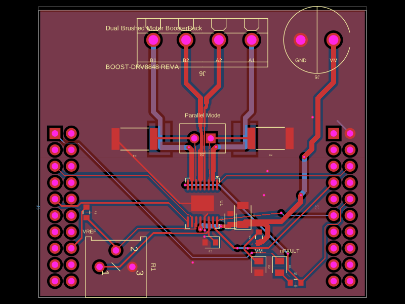 Similar packageMustafaMulla29/ti-boost-drv8848This code defines a hardware layout with 3D models, footprints, and schematic symbols for various electronic components including a potentiometer, motor driver ICs, connectors, capacitors, resistors, LEDs, and copper pours for ground overlays, assembled into a detailed schematic and PCB design.