seveibar/nema17-rp2040-stepper-controller
A tscircuit package created by seveibar.
- Version
- 0.3.1
- License
- unset
- Stars
- 0
index.circuit.tsx
PCB
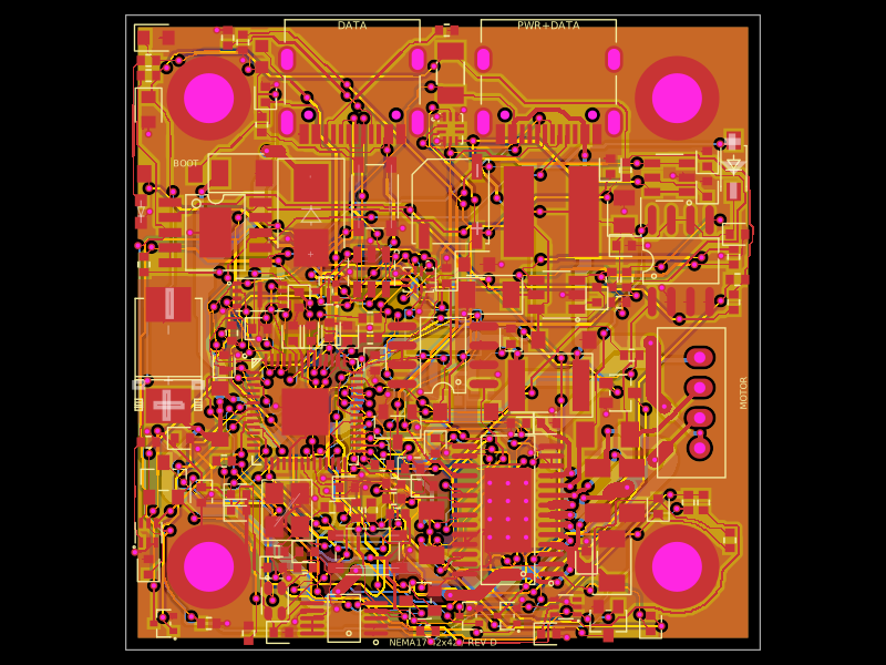
Schematic

import { UnifiedUsbSection } from "./schematic/UnifiedUsbSection";
import { PdPowerGoodSection } from "./schematic/PdPowerGoodSection";
import { autoLayoutSections } from "./schematic/AutoLayoutSections";
import { PdVoltageControlSection } from "./schematic/PdVoltageControlSection";
import { PdBusVoltageMonitorSection } from "./schematic/PdBusVoltageMonitorSection";
import jlcClearanceRules from "./engineering/jlcpcb-clearance-rules.json";
import { ChipDescriptions } from "./schematic/ChipDescriptions";
import { tscircuitBottomLogo } from "./assets/tscircuit-logo-bottom";
import { Drv8825ThermalCopper } from "./schematic/Drv8825ThermalCopper";
import { OptionalEncoderSection } from "./schematic/OptionalEncoderSection";
import { installGroundPourFinalization } from "./routing/ground-pour-selection";
import { CurrentTelemetrySection } from "./schematic/CurrentTelemetrySection";
import { StatusLedSection } from "./schematic/StatusLedSection";
import { FeedbackSection } from "./schematic/FeedbackSection";
import nema17Outline from "./mechanical/nema17-outline.json";
import { savedRouting } from "./routing/saved-routing";
import { ControllerSections } from "./schematic/ControllerSections";
import {
	MotorDriverController,
	MotorDriverControlTraces,
	MotorDriverGroundTraces,
	MotorDriverPassives,
	MotorDriverPowerTraces,
	MotorDriverPrimaryGroundTraces,
	MotorDriverSenseAndControlTraces,
} from "./schematic/MotorDriverCoreSection";
import {
	MotorOutputConnectors,
	MotorOutputTraces,
} from "./schematic/MotorOutputsSection";
import {
	MotorPowerFilteringComponents,
	MotorPowerFilteringGroundTrace,
	MotorPowerFilteringSupplyTrace,
} from "./schematic/MotorPowerFilteringSection";
import {
	MotorPowerPdConnectorGroundTraces,
	MotorPowerPdControllers,
	MotorPowerPdInputTraces,
	MotorPowerPdPassives,
	MotorPowerPdPrimaryGroundTrace,
	MotorPowerPdProtocolTraces,
	MotorPowerPdSupportGroundTraces,
} from "./schematic/MotorPowerPdNegotiationSection";
import { SchematicSheets } from "./schematic/SchematicSheets";
import { ThermalProtectionComponents, ThermalProtectionTraces } from "./schematic/ThermalProtectionSection";

export default function Rp2040MotorController({
	routingDisabled = false,
  routingAlgorithm = savedRouting,
  finalizeGroundPours = true,
}: {
	routingDisabled?: boolean;
  routingAlgorithm?: typeof savedRouting;
  finalizeGroundPours?: boolean;
} = {}) {
	// The DRV8825 footprint intentionally has thermal vias inside its exposed pad.
	// Core's placement check treats via-in-pad as a collision and skips routing.
	return autoLayoutSections(
    <board
      pcbSx={{"& silkscreentext": {visibility: "hidden"}}}
      // Validated routing is replayed only when geometry and connectivity match.
      schMaxTraceDistance={4}
      routeRemaining
      {...(!routingDisabled && finalizeGroundPours ? {ref: installGroundPourFinalization} : {})}
      routingDisabled={routingDisabled}
			isViaInPadAllowed
			layers={4}
      thickness="1.6mm"
			outline={[{x:-21,y:-21},{x:21,y:-21},{x:21,y:21},{x:-21,y:21}]}
			minViaHoleDiameter="0.3mm"
      minViaPadDiameter="0.5mm"
      minViaHoleEdgeToViaHoleEdgeClearance="0.2mm"
      minPlatedHoleDrillEdgeToDrillEdgeClearance="0.45mm"
      minViaEdgeToPadEdgeClearance="0.125mm"
      minTraceWidth={jlcClearanceRules.minimumMm.traceWidth}
      minTraceToPadEdgeClearance={jlcClearanceRules.minimumMm.padToTrace}
      // Native checks currently reuse this field for via-to-pad spacing.
      // checkJlcClearances separately enforces 0.15 mm between component pads.
      minPadEdgeToPadEdgeClearance={jlcClearanceRules.minimumMm.viaToPad}
      minBoardEdgeClearance={jlcClearanceRules.minimumMm.copperToBoardEdge}
			autorouterEffortLevel="2x"
			autorouterVersion="beta_pipeline7"
			autorouter={{
				local: true,
				...(routingAlgorithm ? {algorithmFn:routingAlgorithm} : {}),
				groupMode: "subcircuit",
			}}
		>
			<net name="GND" isGroundNet />
      <UnifiedUsbSection />
			{/* Explicit net names keep labels consistent across the MCU subcircuit and sheets. */}
			<net name="DRIVER_STEP" connectsTo=".MCU > .U1 > .GPIO18" />
			<net name="DRIVER_DIR" connectsTo=".MCU > .U1 > .GPIO19" />
			<net name="DRIVER_RESET" connectsTo=".MCU > .U1 > .GPIO20" />
			<net name="MCU_ENABLE" connectsTo=".MCU > .U1 > .GPIO22" />
			<net name="TEMP_SDA" connectsTo=".MCU > .U1 > .GPIO26_ADC0" />
			<net name="TEMP_SCL" connectsTo=".MCU > .U1 > .GPIO27_ADC1" />
			<SchematicSheets />

			<group pcbX={-5.625} pcbY={-8.25}>
				<ControllerSections />
				<MotorDriverController />
				<MotorPowerPdControllers />
				<MotorOutputConnectors />
				<MotorPowerFilteringComponents />
				<MotorPowerPdPassives />
				<MotorDriverPassives />
				<ThermalProtectionComponents />

				<MotorDriverControlTraces />
				<MotorPowerPdInputTraces />
				<MotorPowerFilteringSupplyTrace />
				<MotorPowerPdProtocolTraces />
				<MotorDriverPowerTraces />
				<MotorDriverPrimaryGroundTraces />
				<MotorPowerPdPrimaryGroundTrace />
				<MotorPowerPdConnectorGroundTraces />
				<MotorPowerFilteringGroundTrace />
				<MotorPowerPdSupportGroundTraces />
				<MotorDriverGroundTraces />
				<MotorOutputTraces />
				<MotorDriverSenseAndControlTraces />
				<ThermalProtectionTraces />
			</group>

			<copperpour
				name="GND_TOP"
        outline={[{x:-20.5,y:-20.5},{x:20.5,y:-20.5},{x:20.5,y:20.5},{x:-20.5,y:20.5}]}
				layer="top"
				connectsTo="net.GND"
				clearance="0.21mm"
				padMargin="0.2mm"
				traceMargin="0.2mm"
				boardEdgeMargin="0.3mm"
				coveredWithSolderMask
			/>
			<copperpour
				name="GND_BOTTOM"
        outline={[{x:-20.5,y:-20.5},{x:20.5,y:-20.5},{x:20.5,y:20.5},{x:-20.5,y:20.5}]}
				layer="bottom"
				connectsTo="net.GND"
				clearance="0.21mm"
				padMargin="0.2mm"
				traceMargin="0.2mm"
				boardEdgeMargin="0.3mm"
				coveredWithSolderMask
			/>

      {(["inner1", "inner2"] as const).map((layer) => (
        <copperpour name={`GND_${layer.toUpperCase()}`}
          outline={[{x:-20.5,y:-20.5},{x:20.5,y:-20.5},{x:20.5,y:20.5},{x:-20.5,y:20.5}]}
          layer={layer} connectsTo="net.GND" clearance="0.21mm"
          padMargin="0.2mm" traceMargin="0.2mm" boardEdgeMargin="0.3mm"
          coveredWithSolderMask />
      ))}

			<group pcbX={0} pcbY={0}>
        <silkscreentext pcbSx={{"& silkscreentext": {visibility: "visible"}}} text="BOOT" pcbX={-17} pcbY={11.2} fontSize="0.6mm" />
        <silkscreentext pcbSx={{"& silkscreentext": {visibility: "visible"}}} text="MOTOR" pcbX={19.9} pcbY={-4} pcbRotation={90} fontSize="0.6mm" />
        <silkscreentext pcbSx={{"& silkscreentext": {visibility: "visible"}}} text="NEMA17 42x42 / REV D" pcbX={0} pcbY={-20.5} fontSize="0.6mm"/>
        {[-15.5,15.5].flatMap(x => [-15.5,15.5].map(y => (
            <chip key={`${x}:${y}`} doNotPlace name={`MH${(x > 0 ? 2 : 0) + (y > 0 ? 1 : 0) + 1}`} pcbX={x} pcbY={y} schSheetName="motor_power"
              pinLabels={{pin1:["GND"]}} connections={{pin1:"net.GND"}}
              footprint={<footprint><courtyardcircle radius={3.05}/><platedhole portHints={["pin1"]} shape="circle" holeDiameter="3.3mm" outerDiameter="5.6mm" /></footprint>} />
        )))}
        <silkscreentext pcbSx={{"& silkscreentext": {visibility: "visible"}}} text="DATA" pcbX={-6} pcbY={20.3} fontSize="0.7mm" />
        <silkscreentext pcbSx={{"& silkscreentext": {visibility: "visible"}}} text="PWR+DATA" pcbX={7} pcbY={20.3} fontSize="0.7mm" />
      </group>
			{/* Explicit source joins also give the MCU sheet the same net labels. */}
			<trace name="LABEL_STEP" from=".MCU > .U1 > .GPIO18" to="net.DRIVER_STEP" schDisplayLabel="DRIVER_STEP" />
			<trace name="LABEL_DIR" from=".MCU > .U1 > .GPIO19" to="net.DRIVER_DIR" schDisplayLabel="DRIVER_DIR" />
			<trace name="LABEL_RESET" from=".MCU > .U1 > .GPIO20" to="net.DRIVER_RESET" schDisplayLabel="DRIVER_RESET" />
			<trace name="LABEL_ENABLE" from=".MCU > .U1 > .GPIO22" to="net.MCU_ENABLE" schDisplayLabel="MCU_ENABLE" />
			<trace name="LABEL_TEMP_SDA" from=".MCU > .U1 > .GPIO26_ADC0" to="net.TEMP_SDA" schDisplayLabel="TEMP_SDA" />
			<trace name="LABEL_TEMP_SCL" from=".MCU > .U1 > .GPIO27_ADC1" to="net.TEMP_SCL" schDisplayLabel="TEMP_SCL" />
      <FeedbackSection />
      <CurrentTelemetrySection />
      <StatusLedSection />
      <OptionalEncoderSection />
      <Drv8825ThermalCopper />
      <ChipDescriptions />
      <PdVoltageControlSection />
      {/* Append new hardware after the validated layout so legacy route IDs remain stable. */}
      <PdBusVoltageMonitorSection />
      <PdPowerGoodSection />
      {/* Ground-plane stitching, independent of capacitor return length constraints. */}
      {[
        { name: "GND_STITCH_DRV_A", x: 0.225, y: -7.96 },
        { name: "GND_STITCH_CORE", x: -4.85, y: 0.31 },
        { name: "GND_STITCH_DRV_B", x: -1.7, y: -6.26 },
      ].map(({name,x,y}) => (
        <via name={name} pcbX={x} pcbY={y}
          holeDiameter="0.3mm" outerDiameter="0.5mm"
          fromLayer="top" toLayer="bottom" connectsTo={["net.GND"]} />
      ))}
		</board>
	);
}
Related Packages
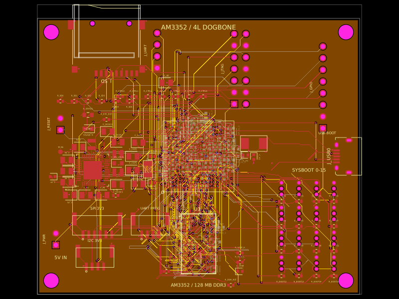 More from this authorseveibar/am3352-dev-board-4layer-dogboneDefines PCB footprints and pin mappings for a TI AM3352ZCZ100 processor, JST GH connectors, and assembly-part lookup helpers for capacitors, resistors, and headers.
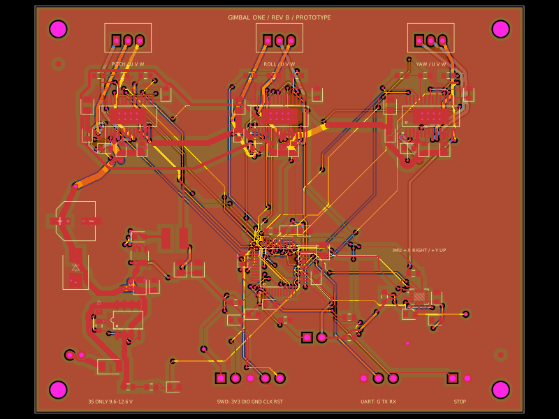 Discover something newmohan-bee/gimbal-one-budget-pcbA 4-layer STM32-based gimbal controller PCB with an onboard LSM6DS3TR-C IMU, three DRV8313 3-phase motor drivers, protected 3S battery input, 3.3 V buck regulation, and SWD/UART control interfaces.