seveibar/keyboard-utils
Based on the code provided, here's a concise summary of the electronic component: A keyboard utility library for parsing and generating keyboard layouts using the Keyboard Layout Editor (KLE) JSON format, with support for generating key matrices, reference designators, and diode routing for keyboard PCBs. Key features: - Parses KLE JSON layouts into key coordinate and metadata objects - Supports various keyboard layouts (60%, ANSI, ISO, Ergodox, etc.) - Generates unique reference designators for keys - Provides utility for adding diode routing in key matrices - TypeScript-based with React and tscircuit integration The library allows keyboard designers to easily convert layout designs into structured, machine-readable keyboard specifications.
- Version
- 0.0.19
- License
- unset
- Stars
- 3
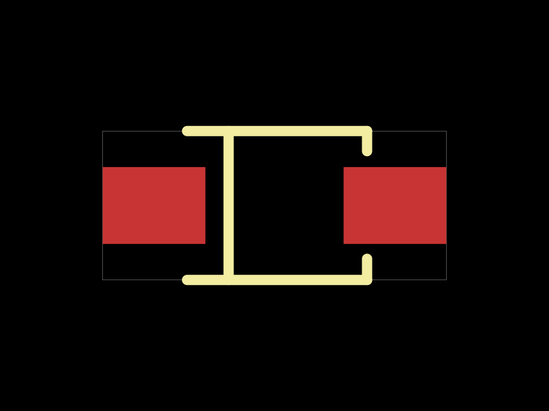
dist/pcb.svg
PCB
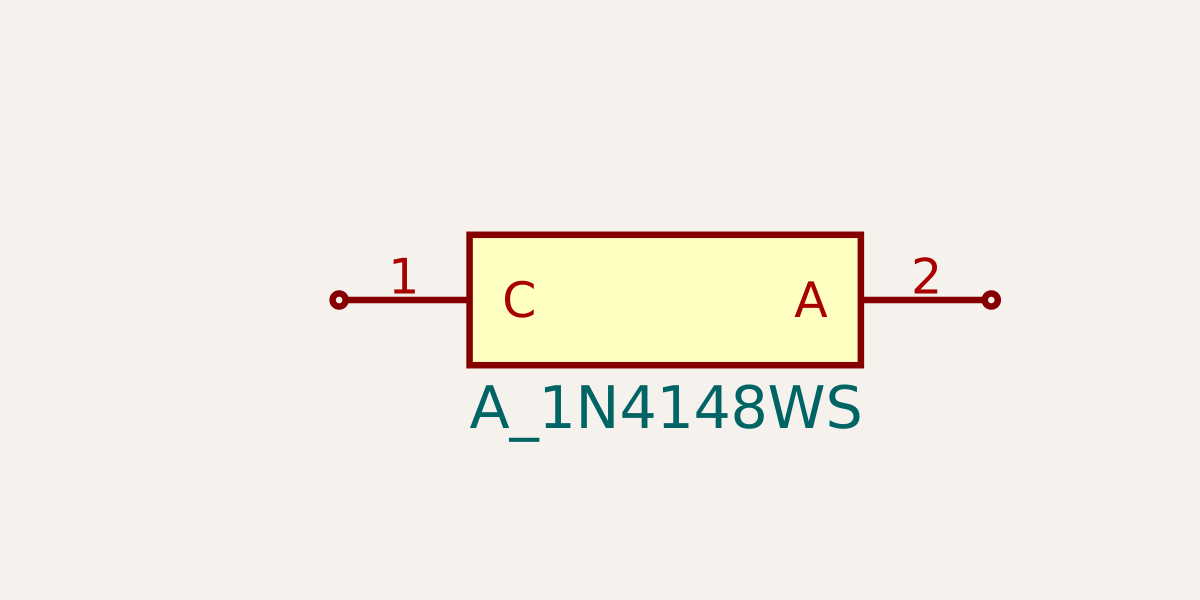
Schematic
<svg xmlns="http://www.w3.org/2000/svg" width="800" height="600" data-software-used-string="@tscircuit/core@0.0.1020"><style></style><rect class="boundary" x="0" y="0" fill="#000" width="800" height="600" data-type="pcb_background" data-pcb-layer="global"/><rect class="pcb-boundary" fill="none" stroke="#fff" stroke-width="0.3" x="149.66755095244628" y="191.30971828825102" width="500.66489809510745" height="217.38056342349796" data-type="pcb_boundary" data-pcb-layer="global"/><rect class="pcb-pad" fill="rgb(200, 52, 52)" x="149.66755095244625" y="243.87383025454733" width="149.66725161734433" height="112.25233949090536" data-type="pcb_smtpad" data-pcb-layer="top"/><rect class="pcb-pad" fill="rgb(200, 52, 52)" x="500.66519743020945" y="243.87383025454733" width="149.66725161734433" height="112.25233949090536" data-type="pcb_smtpad" data-pcb-layer="top"/><path class="pcb-silkscreen pcb-silkscreen-top" d="M 534.8868026895219 408.690281711749 L 534.8868026895219 377.8254502186961" fill="none" stroke="#f2eda1" stroke-width="14.966755095244626" stroke-linecap="round" stroke-linejoin="round" data-pcb-component-id="pcb_component_0" data-pcb-silkscreen-path-id="pcb_silkscreen_path_0" data-type="pcb_silkscreen_path" data-pcb-layer="top"/><path class="pcb-silkscreen pcb-silkscreen-top" d="M 534.8868026895219 191.30971828825102 L 534.8868026895219 220.67673679837603" fill="none" stroke="#f2eda1" stroke-width="14.966755095244626" stroke-linecap="round" stroke-linejoin="round" data-pcb-component-id="pcb_component_0" data-pcb-silkscreen-path-id="pcb_silkscreen_path_1" data-type="pcb_silkscreen_path" data-pcb-layer="top"/><path class="pcb-silkscreen pcb-silkscreen-top" d="M 272.60226222504946 191.30971828825102 L 534.8868026895219 191.30971828825102" fill="none" stroke="#f2eda1" stroke-width="14.966755095244626" stroke-linecap="round" stroke-linejoin="round" data-pcb-component-id="pcb_component_0" data-pcb-silkscreen-path-id="pcb_silkscreen_path_2" data-type="pcb_silkscreen_path" data-pcb-layer="top"/><path class="pcb-silkscreen pcb-silkscreen-top" d="M 272.60226222504946 408.690281711749 L 534.8868026895219 408.690281711749" fill="none" stroke="#f2eda1" stroke-width="14.966755095244626" stroke-linecap="round" stroke-linejoin="round" data-pcb-component-id="pcb_component_0" data-pcb-silkscreen-path-id="pcb_silkscreen_path_3" data-type="pcb_silkscreen_path" data-pcb-layer="top"/><path class="pcb-silkscreen pcb-silkscreen-top" d="M 333.13443513596235 191.30971828825102 L 333.13443513596235 408.690281711749" fill="none" stroke="#f2eda1" stroke-width="14.966755095244626" stroke-linecap="round" stroke-linejoin="round" data-pcb-component-id="pcb_component_0" data-pcb-silkscreen-path-id="pcb_silkscreen_path_4" data-type="pcb_silkscreen_path" data-pcb-layer="top"/></svg>