seveibar/f1c1990s-dev-board
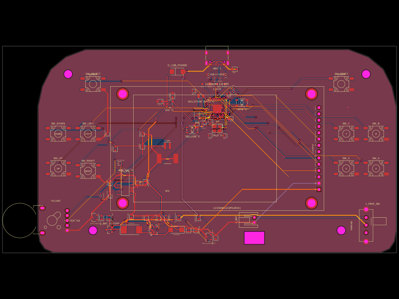
This code manages the entire PCB assembly process for a computer hardware module, including component placement, schematic integration, automated routing, copper pouring, and design rule checks, focused on a four-layer carrier board with integrated support components and connectors.
- Version
- 1.8.0
- License
- unset
- Stars
- 0
fabrication/README.md
# F1C100S dev board fabrication, version 1.8.0

Published package: https://tscircuit.com/seveibar/f1c1990s-dev-board

Fully routed 58 × 48 mm board. Four copper layers, in order: F_Cu, In1_Cu, In2_Cu, B_Cu. FR-4; model thickness 1.4 mm. Four 3.2 mm non-plated mounting holes on 50 × 40 mm centers. Plated through vias: 0.20 mm drills, 0.45 mm pads. Minimum trace width 0.12 mm and clearance 0.10 mm.

Gerbers use millimetres and a common board-centred origin. Upload the Gerbers and both drill files for PCB fabrication. F_Fab is a reference drawing, not copper. All 81 components mount on the top side. Only the top paste stencil is required. JST connectors and the boot header are through-hole parts. The USB-C connector has SMT contacts and plated shell slots; two 0.6 mm non-plated holes locate it. UART TX/RX/GND are bare solder holes, omitted from assembly BOM and pick-and-place.

`bom.csv` and `pick_and_place.csv` are the CLI exports. `assembly-bom.csv` additionally preserves manufacturer part numbers and voltage ratings from the source. All 81 fitted components have explicit JLCPCB supplier numbers. See inventory-check.md for shortages, including the selected 10 µF bulk capacitor. Check pin-1/polarity and supplier rotation conventions in its assembly preview before ordering. Pick-and-place centres and sides were checked against the routed layout; supplier-specific orientation has not been independently qualified.

`routing.dsn` is an editable routing interchange export. The Gerbers come from the already-routed circuit, not a new DSN routing run. `routing-verification.json` and `export-checks.json` record passing connectivity, placement and export checks. The source circuit hash identifies the exact routed input.

Choose and confirm the fabricator's four-layer stackup; the model's 1.4 mm thickness does not specify dielectric spacing. USB differential impedance must be finalized against that stackup. These outputs pass the current software checks; the hardware has not been prototype-tested.
Related Packages
 More from this authorseveibar/testpointsThis hardware consists of a small PCB with five test points arranged linearly, interconnected through a 1kΩ resistor and a 1000pF capacitor, forming a simple RC test configuration.
 Similar packageaura/diy-power-delivery-triggerThis hardware design implements a USB Type-C port with supporting power management and signal conditioning components, including a USB-C connector, a FUSB302 USB-C port controller, ESD protection diodes, a buck converter for 3.3V power regulation, an STM32 microcontroller for control and processing, an RGB LED indicator, push button, terminal block connections, and associated filtering and support components.
 Discover something newabse/gameboy-advanceThis code defines a collection of hardware components, including microcontrollers, sensors, display modules, power management ICs, and passive/passive components, each modeled as 3D symbols with specific footprints, pin configurations, and associated models for PCB and schematic design.