seveibar/f1c1990s-dev-board
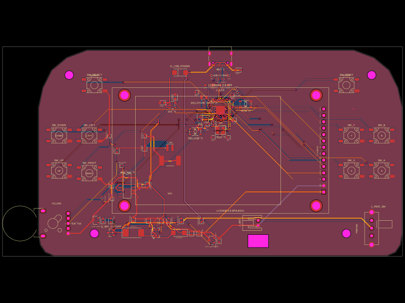
This code manages the entire PCB assembly process for a computer hardware module, including component placement, schematic integration, automated routing, copper pouring, and design rule checks, focused on a four-layer carrier board with integrated support components and connectors.
- Version
- 1.8.0
- License
- unset
- Stars
- 0
capacitor-placement-audit.md
# Capacitor placement audit

Post-improvement review of all 44 capacitors on the native-profile carrier.

**All 15 dedicated processor capacitors now have short, direct top-layer branches to their assigned pins, with zero supply-side vias. Carrier regulator and peripheral capacitors have been moved and reoriented toward their target pins.**

Project checks require at most 3.4 mm pad-to-pin distance, at most 5 mm supply copper, no supply-side vias, and a GND via within 1.3 mm of each ground pad. These are project review limits, not manufacturer specifications. The earlier worst supply branch was 9.46 mm; eight decouplers needed improvement.

## Dedicated processor decouplers

| Capacitor | U1 pin | Pad gap (mm) | Supply copper (mm) | Supply vias | Ground branch to first via (mm) | Assessment |
|---|---:|---:|---:|---:|---:|---|
| C_D4 | 4 | 2.54 | 2.70 | 0 | 0.7 | Pass project placement checks |
| C_D5 | 5 | 2.49 | 2.53 | 0 | 0.69 | Pass project placement checks |
| C_D20 | 20 | 2.49 | 2.49 | 0 | 0.7 | Pass project placement checks |
| C_D22 | 22 | 2.50 | 2.57 | 0 | 0.69 | Pass project placement checks |
| C_D30 | 30 | 2.91 | 3.11 | 0 | 0.7 | Pass project placement checks |
| C_D31 | 31 | 2.62 | 2.82 | 0 | 0.69 | Pass project placement checks |
| C_D32 | 32 | 2.49 | 2.53 | 0 | 0.69 | Pass project placement checks |
| C_D34 | 34 | 2.50 | 2.57 | 0 | 0.69 | Pass project placement checks |
| C_D35 | 35 | 2.65 | 2.86 | 0 | 0.69 | Pass project placement checks |
| C_D36 | 36 | 2.96 | 3.15 | 0 | 0.7 | Pass project placement checks |
| C_D50 | 50 | 1.39 | 1.39 | 0 | 0.69 | Pass project placement checks |
| C_D67 | 67 | 2.51 | 2.61 | 0 | 0.7 | Pass project placement checks |
| C_D71 | 71 | 2.49 | 2.49 | 0 | 0.69 | Pass project placement checks |
| C_D73 | 73 | 2.51 | 2.61 | 0 | 0.69 | Pass project placement checks |
| C_D80 | 80 | 2.49 | 2.49 | 0 | 0.7 | Pass project placement checks |

All 15 supply pads face their assigned pin. Their declared two-port connections were checked against the rendered design. Ground connectivity exists, but no layer is reserved as an uninterrupted ground plane. The available poured copper must be assessed as a return path; these measurements do not establish loop inductance.

## Other 17 module capacitors

| Capacitor | Role | Reference target | Pad gap (mm) |
|---|---|---|---:|
| C_OSCI | oscillator load | Y1.1 | 1.14 |
| C_OSCO | oscillator load | Y1.3 | 1.14 |
| C_B_VCC_HP | rail bulk | U1.4 | 3.33 |
| C_B_VCC_IO | rail bulk | U1.5 | 3.33 |
| C_B_VDD_CORE | rail bulk | U1.22 | 3.18 |
| C_B_VCC_DRAM | rail bulk | U1.30 | 5.37 |
| C_B_VCC_USB | rail bulk | U1.67 | 2.71 |
| C_B_VCC_TV | rail bulk | U1.73 | 7.14 |
| C_B_AVCC | rail bulk | U1.80 | 4.68 |
| C_VRA1 | reference / reset support | U1.81 | 4.94 |
| C_VRA2 | reference / reset support | U1.83 | 5.26 |
| C_SV_H | reference / reset support | U1.36 | 5.49 |
| C_SV_L | reference / reset support | U1.33 | 6.11 |
| C_TV_VRN | reference / reset support | U1.75 | 5.04 |
| C_TV_VRP | reference / reset support | U1.76 | 7.65 |
| C_TV_REF | reference / reset support | U1.76 | 9.51 |
| C_RESET | reference / reset support | U1.70 | 4.84 |

Bulk capacitors serve rails rather than individual pins. Reference/reset and oscillator capacitors need role-specific placement review. The reference target for bulk parts is the nearest same-net processor pin, not a required dedicated connection. Their presence in this table is not a placement approval.

## Twelve carrier capacitors

| Capacitor | Target | Pad gap (mm) | Supply pad closer than ground pad? |
|---|---|---:|---|
| C_SPI | J_SPI.2 | 3.58 | Yes |
| C_I2C | J_I2C.2 | 2.98 | Yes |
| C_U_3V3_IN | U_3V3.8 | 2.41 | Yes |
| C_U_3V3_OUT | U_3V3.1 | 2.41 | Yes |
| C_U_1V8_IN | U_1V8.1 | 1.99 | Yes |
| C_U_1V8_OUT | U_1V8.5 | 1.99 | Yes |
| C_U_1V2_IN | U_1V2.1 | 1.99 | Yes |
| C_U_1V2_OUT | U_1V2.5 | 1.99 | Yes |
| C_FLASH | U_FLASH.8 | 1.79 | Yes |
| C_ESD | U_USB_ESD.5 | 1.67 | Yes |
| C_RGB | D_RGB.2 | 2.38 | Yes |
| C_LED_BUF | U_LED_BUF.8 | 1.83 | Yes |

These are straight-line pad distances, not routed lengths. All twelve carrier capacitors now face their target pins. Regulator and peripheral supply capacitors use explicit pin-target traces. Connector bypass capacitors serve their supply net.

## Limits and references

- No impedance/PDN simulation or hardware measurements.
- Ground-first-via metric follows stored branches incident on the ground pad; null means no via on those branches, not a missing ground connection. Ground pours can add parallel paths.
- Assessment uses relative geometry and an explicit >3.4 mm pad-gap / >5 mm route / any supply-via screening rule; these are review triggers, not Allwinner specified limits.
- Correct orientation and DRC are not sufficient to approve decoupling placement.

[Allwinner F1C100s datasheet, pin assignments](https://linux-sunxi.org/images/b/ba/F1C100s_Datasheet_V1.0.pdf). [TI layout guidance: close placement and short ground return](https://www.ti.com/lit/an/swra640h/swra640h.pdf). The TI guidance supplies general layout principles, not F1C100S-specific numeric limits.
Related Packages
 More from this authorseveibar/testpointsThis hardware consists of a small PCB with five test points arranged linearly, interconnected through a 1kΩ resistor and a 1000pF capacitor, forming a simple RC test configuration.
 Similar packageaura/diy-power-delivery-triggerThis hardware design implements a USB Type-C port with supporting power management and signal conditioning components, including a USB-C connector, a FUSB302 USB-C port controller, ESD protection diodes, a buck converter for 3.3V power regulation, an STM32 microcontroller for control and processing, an RGB LED indicator, push button, terminal block connections, and associated filtering and support components.
 Discover something newabse/gameboy-advanceThis code defines a collection of hardware components, including microcontrollers, sensors, display modules, power management ICs, and passive/passive components, each modeled as 3D symbols with specific footprints, pin configurations, and associated models for PCB and schematic design.