seveibar/ch552t-photo-diode
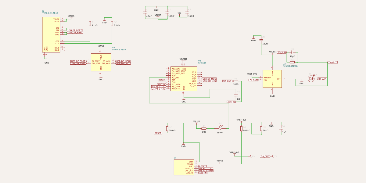
This code defines a compact PCB integrating a CH552T microcontroller, BPX65 photodiode transimpedance amplifier, USB-C connector with power and data traces, decoupling components, passive components, test points, and silkscreen labels.
- Version
- 1.0.2
- License
- unset
- Stars
- 0
index.circuit.tsx
PCB
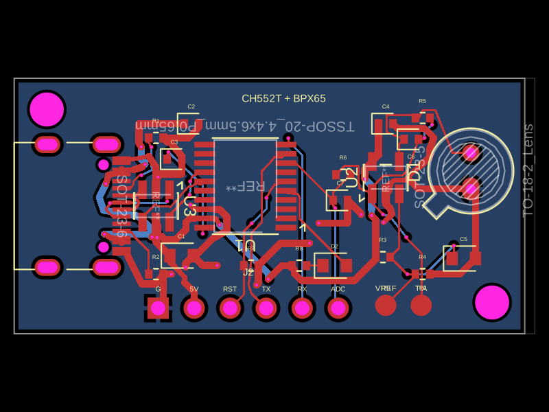
Schematic
import { cloneElement } from "react"
import { SmdUsbC } from "@tsci/seveibar.smd-usb-c"

/*
 * The registry part's CAD offset is correct at 0 degrees, but the offset is
 * not rotated with pcbRotation.  This wrapper applies the equivalent rotated
 * offset for the left-edge, -90 degree placement used on this board.
 */
const LeftEdgeUsbC = (props: Parameters<typeof SmdUsbC>[0]) =>
  cloneElement(SmdUsbC(props), {
    cadModel: {
      objUrl:
        "https://modelcdn.tscircuit.com/easyeda_models/download?uuid=2a4bc2358b36497d9ab2a66ab6419ba3&pn=C165948",
      rotationOffset: { x: 0, y: 0, z: 180 },
      positionOffset: { x: -2.5, y: 0, z: 0 },
    },
  })

const ch552tPins = {
  pin1: "P3_2_AIN3",
  pin2: "P1_4_AIN1_CC1",
  pin3: "P1_5_AIN2_CC2",
  pin4: "P1_6",
  pin5: "P1_7_LED",
  pin6: "RST",
  pin7: "P1_0",
  pin8: "P1_1_AIN0",
  pin9: "P3_1_TXD",
  pin10: "P3_0_RXD",
  pin11: "P3_3",
  pin12: "P3_4",
  pin13: "P3_5",
  pin14: "UDP",
  pin15: "UDM",
  pin16: "P1_3_XO",
  pin17: "P1_2_XI",
  pin18: "GND",
  pin19: "VCC",
  pin20: "V33",
} as const

const opa320Pins = {
  pin1: "OUT",
  pin2: "VNEG",
  pin3: "NONINV",
  pin4: "INV",
  pin5: "VPOS",
} as const

const usblc6Pins = {
  pin1: "DP_PORT",
  pin2: "GND",
  pin3: "DM_PORT",
  pin4: "DM_MCU",
  pin5: "VBUS",
  pin6: "DP_MCU",
} as const

export default () => (
  <board
    name="CH552T_BPX65_SENSOR"
    width="36mm"
    height="18mm"
  >
    <LeftEdgeUsbC
      name="J1"
      pcbX={-12.88}
      pcbY={0}
      pcbRotation={-90}
      schX={-12}
      schY={4}
    />

    <chip
      name="U3"
      manufacturerPartNumber="USBLC6-2SC6"
      supplierPartNumbers={{ jlcpcb: ["C7519"] }}
      footprint="kicad:Package_TO_SOT_SMD/SOT-23-6"
      pinLabels={usblc6Pins}
      schPortArrangement={{
        leftSide: { pins: ["DP_PORT", "DM_PORT"], direction: "top-to-bottom" },
        rightSide: { pins: ["DP_MCU", "DM_MCU"], direction: "top-to-bottom" },
        topSide: { pins: ["VBUS"], direction: "left-to-right" },
        bottomSide: { pins: ["GND"], direction: "left-to-right" },
      }}
      pcbX={-8.0}
      pcbY={0}
      pcbRotation={-90}
      schX={-7.5}
      schY={1.5}
    />

    <chip
      name="U1"
      manufacturerPartNumber="CH552T"
      supplierPartNumbers={{ jlcpcb: ["C111367"] }}
      footprint="kicad:Package_SO/TSSOP-20_4.4x6.5mm_P0.65mm"
      pinLabels={ch552tPins}
      schPortArrangement={{
        leftSide: {
          pins: [
            "P3_2_AIN3",
            "P1_4_AIN1_CC1",
            "P1_5_AIN2_CC2",
            "P1_6",
            "P1_7_LED",
            "RST",
            "P1_0",
            "P1_1_AIN0",
            "P3_1_TXD",
            "P3_0_RXD",
          ],
          direction: "top-to-bottom",
        },
        rightSide: {
          pins: ["P3_3", "P3_4", "P3_5", "UDP", "UDM", "P1_3_XO", "P1_2_XI"],
          direction: "top-to-bottom",
        },
        topSide: { pins: ["VCC", "V33"], direction: "left-to-right" },
        bottomSide: { pins: ["GND"], direction: "left-to-right" },
      }}
      pcbX={-1.7}
      pcbY={1.4}
      pcbRotation={180}
      schX={0}
      schY={0}
    />

    <chip
      name="U2"
      manufacturerPartNumber="OPA320AIDBVR"
      supplierPartNumbers={{ jlcpcb: ["C92494"] }}
      footprint="kicad:Package_TO_SOT_SMD/SOT-23-5"
      pinLabels={opa320Pins}
      schPortArrangement={{
        leftSide: { pins: ["NONINV", "INV"], direction: "top-to-bottom" },
        rightSide: { pins: ["OUT"], direction: "top-to-bottom" },
        topSide: { pins: ["VPOS"], direction: "left-to-right" },
        bottomSide: { pins: ["VNEG"], direction: "left-to-right" },
      }}
      pcbX={8.2}
      pcbY={2.0}
      pcbRotation={90}
      schX={8}
      schY={0}
    />

    <diode
      name="D1"
      photo
      manufacturerPartNumber="BPX 65"
      footprint="kicad:Package_TO_SOT_THT/TO-18-2_Lens"
      pinLabels={{ pin1: "anode", pin2: "cathode" }}
      doNotPlace
      pcbX={14.2}
      pcbY={1.2}
      pcbRotation={90}
      schX={11.5}
      schY={0}
    />

    <resistor name="R1" resistance="5.1k" footprint="0402" pcbX={-8.0} pcbY={4.8} schX={-8.5} schY={5} schRotation={90} />
    <resistor name="R2" resistance="5.1k" footprint="0402" pcbX={-8.0} pcbY={-4.8} schX={-6.5} schY={5} schRotation={90} />

    <capacitor name="C1" capacitance="4.7uF" footprint="0603" pcbX={-6.2} pcbY={-3.5} schX={-3.5} schY={6} schRotation={90} />
    <capacitor name="C2" capacitance="100nF" footprint="0402" pcbX={-5.5} pcbY={5.8} schX={-1.5} schY={6} schRotation={90} />
    <capacitor name="C3" capacitance="100nF" footprint="0402" pcbX={-6.7} pcbY={3.3} schX={0.3} schY={6} schRotation={90} />
    <capacitor name="C4" capacitance="100nF" footprint="0402" pcbX={8.2} pcbY={5.8} schX={7} schY={3.5} schRotation={90} />

    <resistor name="R3" resistance="90.9k" footprint="0402" pcbX={8.0} pcbY={-3.6} schX={5.2} schY={-4.5} schRotation={90} />
    <resistor name="R4" resistance="10k" footprint="0402" pcbX={10.8} pcbY={-4.8} schX={7} schY={-4.5} schRotation={90} />
    <capacitor name="C5" capacitance="1uF" footprint="0603" pcbX={13.7} pcbY={-3.7} schX={8.8} schY={-4.5} schRotation={90} />

    <resistor name="R5" resistance="330k" footprint="0402" pcbX={10.8} pcbY={6.2} schX={9.8} schY={1.5} />
    <capacitor name="C6" capacitance="10pF" footprint="0402" pcbX={10.0} pcbY={4.7} schX={9.8} schY={2.4} />
    <resistor name="R6" resistance="100" footprint="0402" pcbX={5.2} pcbY={2.2} schX={4.7} schY={-0.2} />
    <capacitor name="C7" capacitance="1nF" footprint="0402" pcbX={5.0} pcbY={0.4} schX={4.7} schY={-1.5} schRotation={90} />

    <resistor name="R7" resistance="100k" footprint="0402" pcbX={-1.3} pcbY={-4.2} schX={-1.5} schY={-4.5} schRotation={90} />
    <resistor name="R8" resistance="1k" footprint="0402" pcbX={2.1} pcbY={-4.2} schX={1.8} schY={-4.5} />
    <led name="D2" color="green" footprint="0603" pcbX={4.6} pcbY={-4.2} schX={3.3} schY={-4.5} />

    <pinheader
      name="J2"
      pinCount={6}
      pitch="2.54mm"
      gender="unpopulated"
      doNotPlace
      pinLabels={["GND", "VBUS5", "RST", "UART_TX", "UART_RX", "ADC_IN"]}
      pcbPinLabels={{ pin1: "G", pin2: "5V", pin3: "RST", pin4: "TX", pin5: "RX", pin6: "ADC" }}
      showSilkscreenPinLabels
      pcbX={-1.5}
      pcbY={-7.2}
      pcbOrientation="horizontal"
      schX={0}
      schY={-8}
    />

    <testpoint name="TP1" footprintVariant="pad" padDiameter="1.5mm" pcbX={8.2} pcbY={-7.0} schX={6} schY={-7} />
    <testpoint name="TP2" footprintVariant="pad" padDiameter="1.5mm" pcbX={10.7} pcbY={-7.0} schX={8} schY={-7} />

    <hole name="H1" diameter="2.4mm" pcbX={-15.7} pcbY={6.8} />
    <hole name="H2" diameter="2.4mm" pcbX={15.7} pcbY={-6.8} />

    {/* USB-C power, configuration-channel pull-downs, and shield return. */}
    <trace from=".J1 > .pin3" to="net.VBUS5" thickness="0.5mm" />
    <trace from=".J1 > .pin4" to="net.VBUS5" thickness="0.5mm" />
    <trace from=".J1 > .pin13" to="net.VBUS5" thickness="0.5mm" />
    <trace from=".J1 > .pin14" to="net.VBUS5" thickness="0.5mm" />
    <trace from=".J1 > .pin1" to="net.GND" thickness="0.5mm" />
    <trace from=".J1 > .pin2" to="net.GND" thickness="0.5mm" />
    <trace from=".J1 > .pin15" to="net.GND" thickness="0.5mm" />
    <trace from=".J1 > .pin16" to="net.GND" thickness="0.5mm" />
    <trace from=".J1 > .pin6" to=".R1 > .pin1" />
    <trace from=".R1 > .pin2" to="net.GND" />
    <trace from=".J1 > .pin12" to=".R2 > .pin1" />
    <trace from=".R2 > .pin2" to="net.GND" />

    {/* Both reversible USB 2.0 pin pairs join before the low-capacitance ESD array. */}
    <trace from=".J1 > .pin8" to="net.USB_DP_PORT" thickness="0.25mm" />
    <trace from=".J1 > .pin10" to="net.USB_DP_PORT" thickness="0.25mm" />
    <trace from=".U3 > .pin1" to="net.USB_DP_PORT" thickness="0.25mm" />
    <trace from=".J1 > .pin7" to="net.USB_DM_PORT" thickness="0.25mm" />
    <trace from=".J1 > .pin9" to="net.USB_DM_PORT" thickness="0.25mm" />
    <trace from=".U3 > .pin3" to="net.USB_DM_PORT" thickness="0.25mm" />
    <trace from=".U3 > .pin6" to="net.USB_DP_MCU" thickness="0.25mm" />
    <trace from=".U1 > .pin14" to="net.USB_DP_MCU" thickness="0.25mm" maxViaCount={0} />
    <trace from=".U3 > .pin4" to="net.USB_DM_MCU" thickness="0.25mm" />
    <trace from=".U1 > .pin15" to="net.USB_DM_MCU" thickness="0.25mm" maxViaCount={0} />
    <trace from=".U3 > .pin5" to="net.VBUS5" />
    <trace from=".U3 > .pin2" to="net.GND" />

    {/* CH552T and OPA320 supply decoupling. V33 is only bypassed, not used as a rail. */}
    <trace from=".U1 > .pin19" to="net.VBUS5" thickness="0.4mm" />
    <trace from=".U1 > .pin18" to="net.GND" thickness="0.4mm" />
    <trace from=".U1 > .pin20" to="net.V33" />
    <trace from=".C1 > .pin1" to="net.VBUS5" />
    <trace from=".C1 > .pin2" to="net.GND" />
    <trace from=".C2 > .pin1" to="net.VBUS5" />
    <trace from=".C2 > .pin2" to="net.GND" />
    <trace from=".C3 > .pin1" to="net.V33" />
    <trace from=".C3 > .pin2" to="net.GND" />
    <trace from=".U2 > .pin5" to="net.VBUS5" />
    <trace from=".U2 > .pin2" to="net.GND" />
    <trace from=".C4 > .pin1" to="net.VBUS5" />
    <trace from=".C4 > .pin2" to="net.GND" />

    {/* 0.496 V reference: 5 V * 10 k / (90.9 k + 10 k). */}
    <trace from=".R3 > .pin1" to="net.VBUS5" />
    <trace from=".R3 > .pin2" to="net.VREF_0V5" />
    <trace from=".R4 > .pin1" to="net.VREF_0V5" />
    <trace from=".R4 > .pin2" to="net.GND" />
    <trace from=".C5 > .pin1" to="net.VREF_0V5" />
    <trace from=".C5 > .pin2" to="net.GND" />
    <trace from=".U2 > .pin3" to="net.VREF_0V5" />

    {/* BPX65 TIA: marked anode/pin 1 to GND, cathode/pin 2 to the summing node. */}
    <trace from=".D1 > .pin1" to="net.GND" />
    <trace from=".D1 > .pin2" to="net.PD_SUM" />
    <trace from=".U2 > .pin4" to="net.PD_SUM" />
    <trace from=".R5 > .pin1" to="net.PD_SUM" />
    <trace from=".R5 > .pin2" to="net.TIA_OUT" />
    <trace from=".C6 > .pin1" to="net.PD_SUM" />
    <trace from=".C6 > .pin2" to="net.TIA_OUT" />
    <trace from=".U2 > .pin1" to="net.TIA_OUT" />

    {/* ADC isolation/filter: TIA output -> 100 ohm -> AIN0, with 1 nF at the ADC pin. */}
    <trace from=".R6 > .pin1" to="net.TIA_OUT" />
    <trace from=".R6 > .pin2" to="net.ADC_IN" />
    <trace from=".C7 > .pin1" to="net.ADC_IN" />
    <trace from=".C7 > .pin2" to="net.GND" />
    <trace from=".U1 > .pin8" to="net.ADC_IN" />

    {/* Reset, active-low status LED drive, header, and analog test pads. */}
    <trace from=".U1 > .pin6" to="net.RESET" />
    <trace from=".R7 > .pin1" to="net.RESET" />
    <trace from=".R7 > .pin2" to="net.GND" />
    <trace from=".R8 > .pin1" to="net.VBUS5" />
    <trace from=".R8 > .pin2" to=".D2 > .anode" />
    <trace from=".D2 > .cathode" to=".U1 > .pin5" />
    <trace from=".J2 > .pin1" to="net.GND" />
    <trace from=".J2 > .pin2" to="net.VBUS5" />
    <trace from=".J2 > .pin3" to="net.RESET" />
    <trace from=".J2 > .pin4" to=".U1 > .pin9" />
    <trace from=".J2 > .pin5" to=".U1 > .pin10" />
    <trace from=".J2 > .pin6" to="net.ADC_IN" />
    <trace from=".TP1 > .pin1" to="net.VREF_0V5" />
    <trace from=".TP2 > .pin1" to="net.TIA_OUT" />

    <copperpour
      name="BOTTOM_GND"
      layer="bottom"
      connectsTo="net.GND"
      padMargin="0.25mm"
      traceMargin="0.2mm"
      boardEdgeMargin="0.3mm"
      useThermalReliefs
    />

    <silkscreentext text="CH552T + BPX65" pcbX={1.0} pcbY={7.6} fontSize="0.75mm" />
    <silkscreentext text="VREF" pcbX={8.2} pcbY={-5.8} fontSize="0.55mm" />
    <silkscreentext text="TIA" pcbX={10.7} pcbY={-5.8} fontSize="0.55mm" />
  </board>
)