seveibar/ch552t-photo-diode
This code defines a compact PCB integrating a CH552T microcontroller, BPX65 photodiode transimpedance amplifier, USB-C connector with power and data traces, decoupling components, passive components, test points, and silkscreen labels.
- Version
- 1.0.2
- License
- unset
- Stars
- 0
README.md
# CH552T USB-C BPX65 photodiode board

This tscircuit project is a USB-powered optical sensor built around:

- WCH CH552T USB MCU, TSSOP-20
- TI OPA320AIDBVR precision op-amp, SOT-23-5
- ams OSRAM BPX 65 PIN photodiode, TO-18
- USB-C receptacle with USB 2.0 data and 5.1 kΩ CC pull-downs
- USBLC6-2SC6 low-capacitance USB ESD protection

The compact PCB is 36 × 18 mm, which is 30.8% smaller in both dimensions and
52.1% smaller by area than the original 52 × 26 mm layout. Two diagonal 2.4 mm
mounting holes are retained. The USB-C receptacle is flush with the left board
edge, and its CAD offset is rotated with the footprint so the 3D body aligns
with the connector pads and shell holes.

## Analog signal path

The BPX65 anode (the package-marked lead, footprint pin 1) is grounded. Its
cathode is connected to the OPA320 inverting input. The non-inverting input is
biased at:

```text
VREF = 5 V × 10 kΩ / (90.9 kΩ + 10 kΩ) ≈ 0.496 V
```

The OPA320 is configured as a transimpedance amplifier with 330 kΩ feedback
and 10 pF in parallel:

```text
V_TIA ≈ VREF + I_PHOTO × 330 kΩ
f_feedback ≈ 1 / (2π × 330 kΩ × 10 pF) ≈ 48 kHz
```

The BPX65 data sheet gives a typical 10 µA photocurrent at 1000 lx (standard
light A, 5 V reverse bias). With the default 330 kΩ gain this corresponds to
approximately 3.80 V at `TIA_OUT`. The exact lux transfer is spectrum- and
geometry-dependent, so calibrate the assembled sensor against the intended
light source.

`TIA_OUT` feeds CH552T `AIN0` / P1.1 / physical pin 8 through 100 Ω. A 1 nF
capacitor at the ADC pin isolates sampling kickback and provides a small RF
filter. The CH552T ADC input range is 0 V to VCC and the ADC is 8-bit.

## USB and power

The board runs directly from USB VBUS (nominal 5 V). The CH552T V33 pin is
only bypassed with 100 nF, as required for operation above 3.6 V. USB D+ and
D− route through the USBLC6-2SC6 ESD array with no series resistors; WCH
explicitly says not to put series resistors on CH552 USB pins.

## Header and test points

J2 is an optional 2.54 mm, six-pin unpopulated header:

| Pin | Signal |
| --- | --- |
| 1 | GND |
| 2 | USB 5 V |
| 3 | Active-high RESET |
| 4 | UART TX, P3.1 |
| 5 | UART RX, P3.0 |
| 6 | Filtered ADC input, AIN0 |

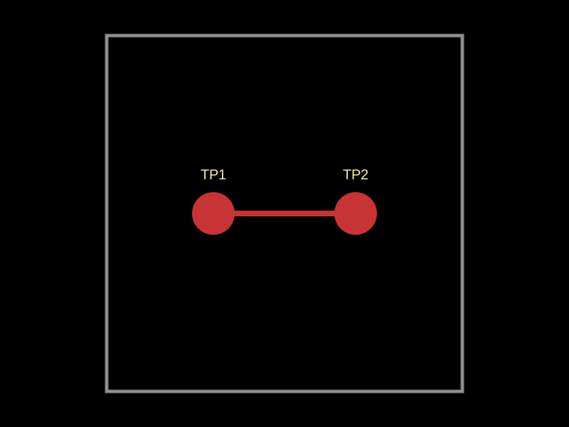
- TP1: 0.496 V reference
- TP2: raw transimpedance-amplifier output
- D2: active-low green firmware status LED on P1.7

## Changing optical gain

R5 sets transimpedance gain and C6 sets the feedback pole. For approximately
ten times more sensitivity, fit 3.3 MΩ and start with 2.2–4.7 pF. For bright
light, fit 33 kΩ and 22–47 pF. Validate stability and saturation with the
actual photodiode, enclosure, cable environment, and optical source.

## Build and export

```sh
npm install
npm run build
tsci export index.circuit.tsx -f schematic-svg -o outputs/schematic.svg
tsci export index.circuit.tsx -f pcb-svg -o outputs/pcb.svg
tsci export index.circuit.tsx -f gerbers -o outputs/gerbers.zip
```

The BPX65 and J2 are marked `doNotPlace`; they are intended for manual
through-hole assembly. Verify the BPX65 package anode marking before soldering.

This is an engineering reference design, not a certified product. Review USB
signal integrity, ESD strategy, enclosure/optical geometry, and fab rules before
production.