seveibar/am3352-dev-board-4layer-dogbone
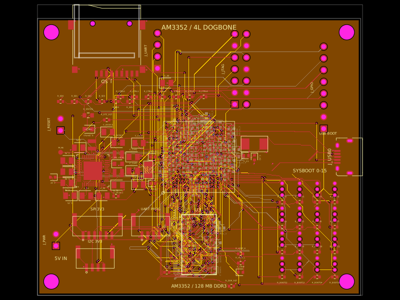
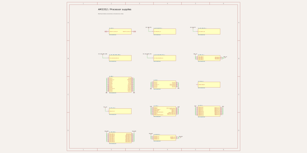
Defines PCB footprints and pin mappings for a TI AM3352ZCZ100 processor, JST GH connectors, and assembly-part lookup helpers for capacitors, resistors, and headers.
- Version
- 0.1.5
- License
- unset
- Stars
- 0
index.circuit.tsx
PCB
Schematic
import { parts, capacitorPart, resistorPart, headerPart } from "./design/assembly-parts"
import { TimingConstraints } from "./design/timing-constraints"
import decouplingPlacement from "./design/decoupling-placement.json"
import { JstGh } from "./components/JstGh"
import { SchematicPages, sch } from "./design/schematic-layout"
import { replayRouter } from "./design/replay-router"
import netNames from "./design/net-names.json"
import { Fragment } from "react"
import { AM3352, ballMap } from "./components/AM3352"
import { TPS65217CRSLR } from "./imports/TPS65217CRSLR"
import { W631GG6MB_12, pinLabels as ramPins } from "./imports/W631GG6MB_12"
import { A_10118194_0001LF } from "./imports/A_10118194_0001LF"
import { TF_01A } from "./imports/TF_01A"
import { phaseForNet, ddrSignals, powerNets } from "./design/routing"

const cpuPower = (s:string):string|undefined => {
  if (/^VSS/.test(s)) return "GND"
  if (s === "VDD_CORE" || s === "VDD_MPU") return s
  if (s === "VDDS_DDR") return "DDR_1V5"
  if (s === "VDDS_RTC") return "RTC_1V8"
  if (/^VDDSHV/.test(s)) return "V3V3"
  if (/^VDDA3P3/.test(s)) return "A3V3"
  if (s === "VDDS" || /^VDDS_(PLL|OSC|SRAM)/.test(s) || /^VDDA1P8/.test(s) || s === "VDDA_ADC") return "V1V8"
}
const cpuSignal = (s:string) => cpuPower(s) ?? ({VREFN:"GND", VREFP:"V1V8",RTC_KALDO_ENn:"GND",VPP:"GND",RTC_PWRONRSTn:"RTC_RESETn"}[s] ?? s)
const usedSignals = new Set([...ddrSignals,"DDR_VREF","DDR_VTP","I2C0_SDA","I2C0_SCL","UART0_TXD","UART0_RXD","TCK","TMS","TDI","TDO","TRSTn","EMU0","EMU1","PWRONRSTn","WARMRSTn","RTC_PWRONRSTn","RTC_KALDO_ENn","PMIC_POWER_EN","VPP","XTALIN","XTALOUT","RTC_XTALIN","RTC_XTALOUT","VREFN","VREFP","MMC0_CLK","MMC0_CMD",...Array.from({length:4},(_,i)=>`MMC0_DAT${i}`),...Array.from({length:16},(_,i)=>`LCD_DATA${i}`),"SPI0_SCLK","SPI0_D0","SPI0_D1","SPI0_CS0","USB0_DP","USB0_DM","USB0_VBUS","USB0_ID", "CAP_VDD_RTC","CAP_VDD_SRAM_CORE","CAP_VDD_SRAM_MPU","CAP_VBB_MPU"])
const link = (ref:string,pin:string,net:string) => <trace key={`${ref}_${pin}`} name={`T_${ref}_${pin}`} routingPhaseIndex={phaseForNet(net)} from={`.${ref} > .${pin}`} to={`net.${net}`} />
function Cap({name,net,value="100nF",x=0,y=0,bottom=false,rotation=0}:{name:string,net:string,value?:string,x?:number,y?:number,bottom?:boolean,rotation?:number}) {
 const placed=bottom?(decouplingPlacement as Record<string,{x:number,y:number,rotation:number}>)[name]:undefined
 if(bottom&&!placed) throw new Error(`Missing optimized placement for ${name}`)
 return <><capacitor {...sch(name)} name={name} {...(name==="C_SYS_LOCAL"?parts.localBypass:capacitorPart(value))} capacitance={value} footprint={name==="C_SYS_LOCAL"?"0603":value.includes("uF")?"0805":"0402"} pcbX={placed?.x??x} pcbY={placed?.y??y} pcbRotation={placed?.rotation??rotation} layer={bottom?"bottom":"top"} />{link(name,"pin1",net)}{link(name,"pin2","GND")}</>
}
function Res({name,a,b,value="10k",x,y,layer="top",rotation=0}:{name:string,a:string,b:string,value?:string,x:number,y:number,layer?:"top"|"bottom",rotation?:number}) {
 return <><resistor {...sch(name)} name={name} {...resistorPart(value)} resistance={value} footprint="0402" pcbX={x} pcbY={y} layer={layer} pcbRotation={rotation} />{link(name,"pin1",a)}{link(name,"pin2",b)}</>
}
const headers = [
 {name:"J_PWR",x:-31,y:-18,pins:["VIN_5V","GND"]},
 {name:"J_UART",x:-9,y:23,pins:["GND","UART0_TXD","UART0_RXD","V3V3"]},
 {name:"J_JTAG",x:9,y:19,pins:["V3V3","TMS","GND","TCK","GND","TDO","GND","TDI","TRSTn","GND","EMU0","EMU1","WARMRSTn","GND"]},
 {name:"J_GPIO",x:27,y:15,pins:["V3V3","GND","SPI0_SCLK","SPI0_D0","SPI0_D1","SPI0_CS0","I2C0_SDA","I2C0_SCL"]},

 {name:"J_RESET",x:-30,y:7,pins:["WARMRSTn","GND"]},
]
const powerPins:Record<string,string> = {AC:"VIN_5V",SYS1:"SYS_5V",SYS2:"SYS_5V",VIN_DCDC1:"SYS_5V",VIN_DCDC2:"SYS_5V",VIN_DCDC3:"SYS_5V",VINLDO:"SYS_5V",LS1_IN:"SYS_5V",LS2_IN:"SYS_5V",VLDO1:"RTC_1V8",VLDO2:"A3V3",LS1_OUT:"V1V8",LS2_OUT:"V3V3",VDCDC1:"DDR_1V5",VDCDC2:"VDD_MPU",VDCDC3:"VDD_CORE",PWR_EN:"PMIC_POWER_EN",PGOOD:"PWRONRSTn",nRESET:"RTC_RESETn",SDA:"I2C0_SDA",SCL:"I2C0_SCL",VIO:"V3V3",PGND:"GND",AGND:"GND",EP:"GND",TS:"PMIC_TS",INT_LDO:"PMIC_INT_LDO",BYPASS:"PMIC_BYPASS",PB_IN:"PMIC_PB",USB:"GND"}
const ramNet = (s:string):string|undefined => {
 if (/^VSS/.test(s)) return "GND"
 if (/^VDD/.test(s)) return "DDR_1V5"
 if (/^VREF/.test(s)) return "DDR_VREF"
 if (/^DQL\d/.test(s)) return `DDR_D${s.slice(3)}`
 if (/^DQU\d/.test(s)) return `DDR_D${8+Number(s.slice(3))}`
 if (/^A\d+$/.test(s) || /^BA\d/.test(s)) return `DDR_${s}`
 return ({ODT:"DDR_ODT",CKE:"DDR_CKE",CK:"DDR_CK",N_CK:"DDR_CKn",N_CS:"DDR_CSn0",N_RESET:"DDR_RESETn",N_RAS:"DDR_RASn",N_CAS:"DDR_CASn",N_WE:"DDR_WEn",DML:"DDR_DQM0",DMU:"DDR_DQM1",DQSL:"DDR_DQS0",N_DQSl:"DDR_DQSn0",DQSU:"DDR_DQS1",N_DQSU:"DDR_DQSn1",ZQ:"DDR_ZQ"} as Record<string,string>)[s]
}
export default function Board() {
 const supplies=Object.entries(ballMap).filter(([,s])=>cpuPower(s)&&cpuPower(s)!=="GND")
 return <board width={70} height={60} layers={4} thickness={1.2} minTraceWidth={0.1} minTraceToPadEdgeClearance={0.1} minViaPadDiameter={0.3} minViaHoleDiameter={0.15} routeRemaining={false} schAutoLayoutEnabled={false} schTraceAutoLabelEnabled schMaxTraceDistance={2} title="AM3352 • four-layer dogbone version">
   <TimingConstraints />
   <copperpour name="GND_PLANE" layer="inner1" connectsTo="net.GND" unbroken clearance={0.13} boardEdgeMargin={0.4}/>
   {netNames.map(name=><net name={name} routingPhaseIndex={phaseForNet(name)}/>)}
   <AM3352 {...sch("U1")} name="U1" noSchematicRepresentation pcbX={0} pcbY={0} />
   <TPS65217CRSLR {...sch("U2")} name="U2" noSchematicRepresentation pcbX={-23} pcbY={-3} />
   <W631GG6MB_12 {...sch("U3")} name="U3" noSchematicRepresentation pcbX={0} pcbY={-19} />
   <A_10118194_0001LF {...sch("J_USB0")} name="J_USB0" pcbX={31} pcbY={0} pcbRotation={90} />
   {["USB0_VBUS","USB0_DM","USB0_DP","USB0_ID","GND","GND","GND","GND","GND"].map((n,i)=>link("J_USB0",`pin${i+1}`,n))}
   <TF_01A {...sch("J_SD")} name="J_SD" pcbX={-20} pcbY={23.5} pcbRotation={180} />
   {Object.entries(ballMap).filter(([,s])=>cpuPower(s)||usedSignals.has(s)).map(([ball,s])=>link("U1",ball,cpuSignal(s)))}
   {Object.entries(powerPins).map(([pin,net])=>link("U2",pin,net))}
   {Object.entries(ramPins).map(([pin,labels])=>{const net=ramNet(labels[1]??"");return net?link("U3",pin,net):null})}
   {headers.map(h=><Fragment key={h.name}><pinheader {...sch(h.name)} name={h.name} {...headerPart(h.name,h.pins.length)} pinCount={h.pins.length} doubleRow={h.name==="J_JTAG"} pitch={2.54} pcbX={h.x} pcbY={h.y} pcbRotation={90} />{h.pins.map((n,i)=>link(h.name,`pin${i+1}`,n))}</Fragment>)}
   {["MMC0_DAT2","MMC0_DAT3","MMC0_CMD","V3V3","MMC0_CLK","GND","MMC0_DAT0","MMC0_DAT1","SD_CD","GND","GND","GND","GND"].map((n,i)=>link("J_SD",`pin${i+1}`,n))}
   {supplies.map(([ball,s],i)=><Cap key={ball} name={`C_U1_${ball}`} net={cpuPower(s)!} bottom />)}
   {["DDR_1V5","VDD_MPU","VDD_CORE"].map((rail,i)=><Fragment key={rail}>
    <inductor {...sch(`L${i+1}`)} name={`L${i+1}`} {...parts.inductor} inductance="2.2uH" footprint={<footprint>{[-1,1].map((sign,j)=><smtpad portHints={[`pin${j+1}`]} shape="rect" pcbX={sign*0.8} pcbY={0} width={0.8} height={1.8}/>)}<courtyardrect pcbX={0} pcbY={0} width={2.9} height={2.3}/></footprint>} pcbX={[-17.5,-17.5,-23.2][i]} pcbY={[-3.5,0.5,2.6][i]} pcbRotation={i===2?90:0}/>
    {link("U2",`L${i+1}`,`SW${i+1}`)}{link(`L${i+1}`,"pin1",`SW${i+1}`)}{link(`L${i+1}`,"pin2",rail)}
    <Cap name={`C_DCDC${i+1}`} net={rail} value="22uF" x={[-17.5,-17.5,-19.7][i]} y={[-6.1,3.1,5.4][i]}/>
   </Fragment>)}
   {["VIN_5V","SYS_5V","RTC_1V8","A3V3","V1V8","V3V3","PMIC_BYPASS","PMIC_INT_LDO"].map((n,i)=><Cap key={n} name={`C_P${i}`} net={n} value={n==="PMIC_INT_LDO"?"100nF":"4.7uF"} x={[-20.8,-26.1,-24.4,-28,-28.6,-28.6,-28.6,-31.7][i]} y={[-8.4,2,-8.4,-8.4,-0.8,-3.2,-5.6,-4.4][i]} rotation={i===1||i>=3?180:0}/>)}
   {Array.from({length:16},(_,i)=><Cap key={i} name={`C_DDR${i}`} net="DDR_1V5" bottom/>)}
   <Res name="R_VREF_H" a="DDR_1V5" b="DDR_VREF" value="10k" x={9} y={-21}/>
   <Res name="R_VREF_L" a="DDR_VREF" b="GND" value="10k" x={9} y={-23}/>
   <Cap name="C_VREF" net="DDR_VREF" x={9} y={-25}/>
   <Res name="R_ZQ" a="DDR_ZQ" b="GND" value="240" x={-7} y={-25}/>
   <Res name="R_VTP" a="DDR_VTP" b="GND" value="49.9" x={-1.29} y={-4.8} layer="bottom"/>
   <Res name="R_DDR_RST" a="DDR_RESETn" b="GND" value="10k" x={7} y={-28}/>
   {["I2C0_SDA","I2C0_SCL","PWRONRSTn","WARMRSTn","TRSTn","EMU0","EMU1"].map((n,i)=><Res key={n} name={`R_CTRL${i}`} a={n} b="V3V3" value={i<2?"4.7k":"10k"} x={-17+i*3} y={13}/>)}
   <Res name="R_RTC_RST" a="RTC_RESETn" b="RTC_1V8" x={-20} y={8}/>
   <Res name="R_TS" a="PMIC_TS" b="GND" value="10k" x={-18} y={-8.5}/>
   {["CAP_VDD_RTC","CAP_VDD_SRAM_CORE","CAP_VDD_SRAM_MPU","CAP_VBB_MPU"].map((n,i)=><Cap key={n} name={`C_CAP${i}`} net={n} value="1uF" x={i===1||i===2?-14.25:-13} y={-6+i*3}/>)}
   <crystal {...sch("Y1")} name="Y1" {...parts.xtal24} frequency="24MHz" loadCapacitance="18pF" footprint={<footprint><smtpad portHints={["pin1"]} shape="rect" width={1.9} height={2.4} pcbX={-2.05}/><smtpad portHints={["pin2"]} shape="rect" width={1.9} height={2.4} pcbX={2.05}/><courtyardrect pcbX={0} pcbY={0} width={6.5} height={3.9}/><silkscreenrect pcbX={0} pcbY={0} width={5.8} height={3.4}/></footprint>} pcbX={12} pcbY={2.8}/>
   {link("Y1","pin1","XTALIN")}{link("Y1","pin2","XTALOUT")}
   <Cap name="C_X1" net="XTALIN" value="22pF" x={10.2} y={0.3}/><Cap name="C_X2" net="XTALOUT" value="22pF" x={12} y={-0.15} rotation={270}/>
   {/* Epson FC-135: no circuit patterns between the two lands. */}
   <keepout shape="rect" pcbX={-11} pcbY={-2.8} width={1.8} height={1.5} layers={["top"]} allowPlacements />
      <crystal {...sch("Y2")} name="Y2" {...parts.xtal32} frequency="32.768kHz" loadCapacitance="12.5pF" footprint={<footprint><smtpad portHints={["pin1"]} shape="rect" width={1} height={1.8} pcbX={-1.25}/><smtpad portHints={["pin2"]} shape="rect" width={1} height={1.8} pcbX={1.25}/><courtyardrect pcbX={0} pcbY={0} width={4} height={2.3}/><silkscreenrect pcbX={0} pcbY={0} width={3.8} height={2}/></footprint>} pcbX={-11} pcbY={-2.8} pcbRotation={270}/>
   {link("Y2","pin1","RTC_XTALIN")}{link("Y2","pin2","RTC_XTALOUT")}
   <Cap name="C_RTCX1" net="RTC_XTALIN" value="18pF" x={-10} y={0} rotation={0}/><Cap name="C_RTCX2" net="RTC_XTALOUT" value="18pF" x={-10} y={-5.75} rotation={0}/>
   {["MMC0_CMD","MMC0_DAT0","MMC0_DAT1","MMC0_DAT2","MMC0_DAT3","SD_CD"].map((n,i)=><Res key={n} name={`R_SD${i}`} a={n} b="V3V3" value="47k" x={-30+i*3} y={12}/>)}
   <Cap name="C_SD" net="V3V3" value="10uF" x={-7} y={16}/>
   {/* SYSBOOT[15:0] use LCD_DATA balls. Populate straps after selecting the ROM boot order. */}
   {Array.from({length:16},(_,i)=><Fragment key={i}><pinheader {...sch(`J_BOOT${i}`)} name={`J_BOOT${i}`} {...headerPart(`J_BOOT${i}`,3)} pinCount={3} pitch={1.27} footprint={<footprint>{[1,2,3].map(n=><platedhole portHints={[`pin${n}`]} shape="circle" holeDiameter={0.65} outerDiameter={0.95} pcbX={(n-2)*1.27} pcbY={0}/>)}<courtyardrect pcbX={0} pcbY={0} width={4.01} height={2.3}/></footprint>} pcbRotation={90} pcbX={18+(i%4)*3.8} pcbY={-7-Math.floor(i/4)*5.4} />{link(`J_BOOT${i}`,"pin1","V3V3")}{link(`J_BOOT${i}`,"pin3","GND")}<Res name={`R_BOOT${i}`} a={`LCD_DATA${i}`} b={`BOOT_SEL${i}`} value="100k" x={18+(i%4)*3.8} y={-9.8-Math.floor(i/4)*5.4}/>{link(`J_BOOT${i}`,"pin2",`BOOT_SEL${i}`)}</Fragment>)}
   <resistor {...sch("R_STATUS")} name="R_STATUS" {...parts.res1k} resistance="1k" footprint="0603" pcbX={-24} pcbY={9}/>
   {/* C965805 uses pin 1 = cathode; rotate to retain the existing cathode pad on the right. */}
   <led {...sch("D_STATUS")} name="D_STATUS" {...parts.led} pinLabels={{pin1:["cathode","neg"],pin2:["anode","pos"]}} color="green" footprint="0603" pcbX={-24} pcbY={6} pcbRotation={180}/>
   {link("R_STATUS","pin1","V3V3")}
   <trace name="STATUS_LED" routingPhaseIndex={3} from=".R_STATUS > .pin2" to=".D_STATUS > .anode" />
   {link("D_STATUS","cathode","GND")}
   <testpoint {...sch("TP_PB")} name="TP_PB" footprintVariant="pad" padShape="circle" padDiameter={1} pcbX={-30} pcbY={1}/>{link("TP_PB","pin1","PMIC_PB")}
   <Cap name="C_SYS_LOCAL" net="SYS_5V" value="4.7uF" x={-17.5} y={-1.5}/>
   {[-32,32].flatMap(x=>[-27,27].map(y=><hole name={`H_${x}_${y}`} diameter={3.2} pcbX={x} pcbY={y}/>))}
   <silkscreentext text="AM3352 / 4L DOGBONE" pcbX={0} pcbY={28} fontSize={1.4}/>
   <silkscreentext text="AM3352 / 128 MB DDR3" pcbX={0} pcbY={-28} fontSize={1}/>
   <silkscreentext text="5V IN" pcbX={-30} pcbY={-22} fontSize={1}/>
   <silkscreentext text="SYSBOOT 0-15" pcbX={24} pcbY={-3} fontSize={1}/>
   {/* Locking cable interfaces, bottom-left quadrant; pin 1 marked on silk. */}
   {[
    {name:"J_SPI",x:-22,y:-15,pins:["GND","V3V3","SPI0_SCLK","SPI0_D0","SPI0_D1","SPI0_CS0"]},
    {name:"J_I2C",x:-22.5,y:-22,pins:["GND","V3V3","I2C0_SDA","I2C0_SCL"]},
    {name:"J_PROG",x:-10.5,y:-15,pins:["GND","UART0_TXD","UART0_RXD","V3V3"]},
   ].map(h=><Fragment key={h.name}><JstGh {...sch(h.name)} name={h.name} pins={h.pins} pcbX={h.x} pcbY={h.y}/>{[...h.pins,"GND","GND"].map((n,i)=>link(h.name,`pin${i+1}`,n))}</Fragment>)}
   <silkscreentext text="SPI 3V3" pcbX={-22} pcbY={-11.3} fontSize={0.8}/>
   <silkscreentext text="I2C 3V3" pcbX={-22.5} pcbY={-18.3} fontSize={0.8}/>
   <silkscreentext text="UART PROG" pcbX={-10.5} pcbY={-11.3} fontSize={0.7}/>
   <silkscreentext text="USB BOOT" pcbX={28} pcbY={5.1} fontSize={0.75}/>
   {[16,17].map(i=><Cap key={i} name={`C_DDR${i}`} net="DDR_1V5" bottom/>)}
   <SchematicPages />
   {["clock-and-reference", "ddr", "interfaces", "control-and-boot", "power", "ground"].map((name,i)=><autoroutingphase key={name} name={name} phaseIndex={i+1} autorouter={{algorithmFn:replayRouter}}/>)}
 </board>
}
Related Packages
 More from this authorseveibar/wifi-test-board-1
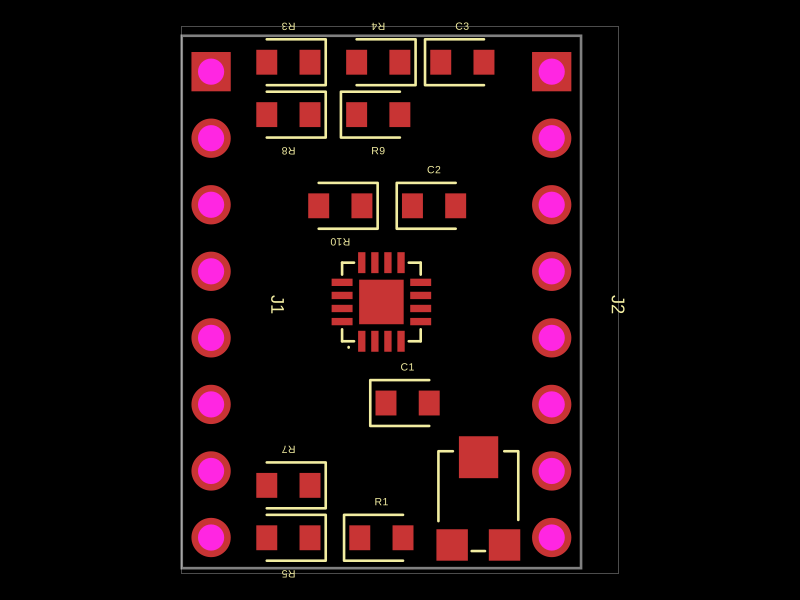 Similar packageAyushjhawar8/stepper-mini-motorThis code defines a schematic and PCB layout for a motor driver IC (TC78H670FTG) with associated passive components, power supply capacitors, resistors, headers, and mechanical footprints, all mapped with specific pin configurations and connections.
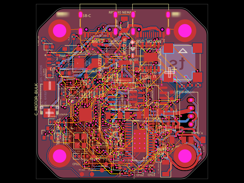 Discover something newimrishabh18/rp2040-motor-controllerA four-layer RP2040-based NEMA17 stepper controller with USB-C power/data, CH224K USB-PD negotiation, DRV8825 dual H-bridge drive, current/temperature telemetry, RGB status LED, buzzer alarm, QSPI flash, and optional AS5600 encoder.