seveibar/am3352-dev-board-4layer-dogbone
Defines PCB footprints and pin mappings for a TI AM3352ZCZ100 processor, JST GH connectors, and assembly-part lookup helpers for capacitors, resistors, and headers.
- Version
- 0.1.5
- License
- unset
- Stars
- 0
design/assembly-supplier-imports/DFE201612E_2R2M_P2.tsx
import type { ChipProps } from "@tscircuit/props"

const pinLabels = {
  pin1: ["pin1"],
  pin2: ["pin2"]
} as const

export const DFE201612E_2R2M_P2 = (props: ChipProps<typeof pinLabels>) => {
  return (
    <chip
      pinLabels={pinLabels}
      symbol={
        <symbol>
          <port name="pin2" pinNumber={2} aliases={["2"]} direction="right" schX={0.4} schY={0} schStemLength={0.06} />
          <port name="pin1" pinNumber={1} aliases={["1"]} direction="left" schX={-0.4} schY={0} schStemLength={0.06} />
          <schematicpath svgPath="M -0.33766 0.00136 A 0.08 0.078 0 1 0 -0.17836 0.00128" strokeColor="#880000" />
          <schematicpath svgPath="M -0.168 0.00142 A 0.08 0.078 0 1 0 -0.0087 0.00132" strokeColor="#880000" />
          <schematicpath svgPath="M 0.00134 0.00142 A 0.08 0.078 0 1 0 0.16064 0.00132" strokeColor="#880000" />
          <schematicpath svgPath="M 0.174 0.00138 A 0.08 0.078 0 1 0 0.3333 0.00128" strokeColor="#880000" />
        </symbol>
      }
      supplierPartNumbers={{
  "jlcpcb": [
    "C337893"
  ]
}}
      manufacturerPartNumber="DFE201612E-2R2M=P2"
      footprint={<footprint>
        <smtpad portHints={["pin2"]} pcbX="0.999998mm" pcbY="0mm" width="1.1999976mm" height="1.7999964mm" shape="rect" />
<smtpad portHints={["pin1"]} pcbX="-0.999998mm" pcbY="0mm" width="1.1999976mm" height="1.7999964mm" shape="rect" />
<silkscreenpath route={[{"x":-0.4999990000000025,"y":1.1999975999999606},{"x":-1.54998420000004,"y":1.1999975999999606}]} />
<silkscreenpath route={[{"x":-0.4999990000000025,"y":-1.1999976000000743},{"x":-1.54998420000004,"y":-1.1999976000000743}]} />
<silkscreenpath route={[{"x":0.49999899999988884,"y":1.1999975999999606},{"x":1.54998420000004,"y":1.1999975999999606}]} />
<silkscreenpath route={[{"x":0.49999899999988884,"y":-1.1999976000000743},{"x":1.54998420000004,"y":-1.1999976000000743}]} />
<silkscreenpath route={[{"x":-1.8999708000001192,"y":0.9999979999998914},{"x":-1.8999708000001192,"y":-0.9999979999998914}]} />
<silkscreenpath route={[{"x":1.8999708000000055,"y":0.9999979999998914},{"x":1.8999708000000055,"y":-0.9999979999998914}]} />
<silkscreenpath route={[{"x":-1.54998420000004,"y":1.1999975999999606},{"x":-1.6999712000001637,"y":1.1999975999999606},{"x":-1.8999708000001192,"y":0.9999979999998914}]} />
<silkscreenpath route={[{"x":-1.54998420000004,"y":-1.1999976000000743},{"x":-1.6999712000001637,"y":-1.1999976000000743},{"x":-1.8999708000001192,"y":-0.9999979999998914}]} />
<silkscreenpath route={[{"x":1.54998420000004,"y":1.1999975999999606},{"x":1.6999711999999363,"y":1.1999975999999606},{"x":1.8999708000000055,"y":0.9999979999998914}]} />
<silkscreenpath route={[{"x":1.54998420000004,"y":-1.1999976000000743},{"x":1.6999711999999363,"y":-1.1999976000000743},{"x":1.8999708000000055,"y":-0.9999979999998914}]} />
<silkscreentext text="{NAME}" pcbX="0.009398mm" pcbY="2.1938mm" anchorAlignment="center" fontSize="1mm" />
<courtyardoutline outline={[{"x":-2.1456020000000535,"y":1.4437999999998965},{"x":2.164397999999892,"y":1.4437999999998965},{"x":2.164397999999892,"y":-1.4438000000001239},{"x":-2.1456020000000535,"y":-1.4438000000001239},{"x":-2.1456020000000535,"y":1.4437999999998965}]} />
      </footprint>}
      cadModel={{
        objUrl: "https://modelcdn.tscircuit.com/easyeda_models/assets/C337893.obj?uuid=969fb22dc7094eac9379f530d4c94913",
        stepUrl: "https://modelcdn.tscircuit.com/easyeda_models/assets/C337893.step?uuid=969fb22dc7094eac9379f530d4c94913",
        pcbRotationOffset: 0,
        modelOriginPosition: { x: 0, y: 0, z: -0.475 },
      }}
      {...props}
    />
  )
}
Related Packages
 More from this authorseveibar/wifi-test-board-1
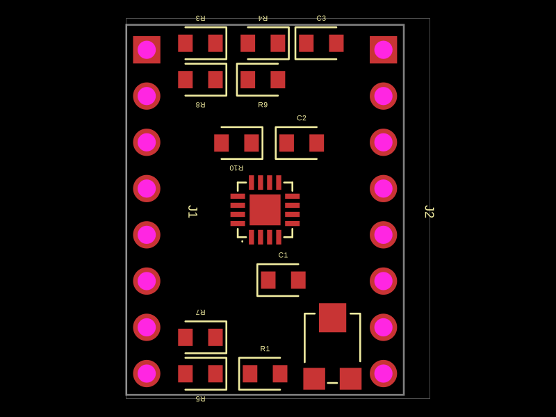 Similar packageAyushjhawar8/stepper-mini-motorThis code defines a schematic and PCB layout for a motor driver IC (TC78H670FTG) with associated passive components, power supply capacitors, resistors, headers, and mechanical footprints, all mapped with specific pin configurations and connections.
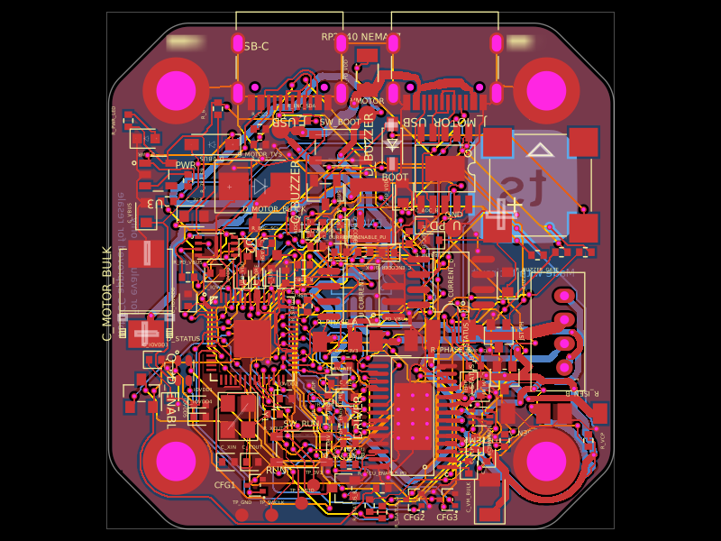 Discover something newimrishabh18/rp2040-motor-controllerA four-layer RP2040-based NEMA17 stepper controller with USB-C power/data, CH224K USB-PD negotiation, DRV8825 dual H-bridge drive, current/temperature telemetry, RGB status LED, buzzer alarm, QSPI flash, and optional AS5600 encoder.