seveibar/am3352-dev-board-4layer-dogbone
Defines PCB footprints and pin mappings for a TI AM3352ZCZ100 processor, JST GH connectors, and assembly-part lookup helpers for capacitors, resistors, and headers.
- Version
- 0.1.5
- License
- unset
- Stars
- 0
FABRICATION-REVIEW.md
# Fabrication review — electrical work remains

Assembly corrections validated locally on 2026-09-20, using tscircuit 0.0.2594 / core 0.0.1944. Circuit SHA-256: `2e87a0446358f7054a1bba368ae394a62fa0aa878933c439b65452f5225fda89`. This local assembly revision has not been published to the registry or ordered.

## Assembly corrections completed

All 184 populated board components now have manufacturer part numbers. The 163 SMT placements have JLCPCB codes and explicit supplier-library orientation mappings; the 21 through-hole headers have a separate manual-assembly BOM. TP_PB is a bare test pad. The LED's anode/cathode numbering difference is handled explicitly in the placement exporter.

L1–L3, Y1 and Y2 use checked manufacturer land patterns. U1 and the crystals have courtyards, JST insertion directions are specified, and the boot-header housing envelopes were checked against nearby parts. The RTC crystal has an enforced top-copper keepout between its lands. Nearby component placements and copper were repaired to fit these footprints, retaining all DDR signal routes. See [assembly files and sources](assembly/README.md).

The selected four-pin JST part C161692 had only two pieces in the saved JLC search-index snapshot. Replenish/pre-order or consign these exact connectors, or install them manually; no inventory is reserved. The supplier's final assembly preview has not been approved.

## Rechecked and passed

- Native `tsci build --site`: zero DRC errors.
- Independent copper geometry: all 138 nets connected, zero clearance violations under the 0.1 mm rule (3 µm comparison tolerance).
- All 19 independent DDR length checks pass; maximum group skew remains 0.019585 mm including used via barrels. All 46 matched nets pass topology checks.
- All 421 vias clear every SMT pad on both faces by at least 0.1 mm, including same-net pads. No filled/capped-via sites are required.
- Four-layer usage, saved-routing consistency, decoupling placement, TypeScript and connectivity tooling checks pass.
- Strict assembly export: 163 SMT placements, zero unresolved rotations; all BOM/CPL references match.

## JLCPCB via drill confirmed

JLCPCB publishes 0.15 mm through-drill capability for multilayer boards and a minimum 0.25 mm pad for those vias. Our 0.30 mm pad meets that limit and the preferred 0.15 mm pad-minus-hole diameter difference. Select the 0.15 mm via option; an extra charge applies. The current 0.1 mm trace/space requires the compatible 1 oz outer-copper process. [JLCPCB capabilities](https://jlcpcb.com/capabilities/pcb-capabilities).

Current minimum via drill-edge gap is 0.253 mm, above JLCPCB's published 0.20 mm limit. Nominal radial annulus is 0.075 mm; board-thickness/drill ratio is 8:1. Exact stackup and order DFM remain to be approved.

## Remaining electrical/layout findings

1. **DDR reference planes and impedance.** The stack is signal / ground / signal / signal. DDR uses top, inner2 and bottom; bottom lacks a directly adjacent continuous reference plane. Dielectric thicknesses and controlled impedance have not been selected. TI requires adjacent reference planes and gives a signal/ground/power/signal four-layer reference stack. Length matching does not qualify the current return paths. [AM335x datasheet, §7.7.2.3.3.3 and Tables 7-61/62](https://www.ti.com/lit/ds/symlink/am3352.pdf).

2. **PMIC power layout.** SW1–SW3, VIN_5V, SYS_5V, VDD_MPU and VDD_CORE still use 0.1 mm trace segments. Load-current, voltage-drop, thermal, input-bypass, feedback and return-loop analysis remains open. Actual inductors are now selected (2.4 A saturation, 1.8 A temperature-rise rating, 0.116 Ω maximum DCR), but that does not resolve the copper/current budget. Review effective capacitor values under bias and local converter input bypassing against TI's layout. [TPS65217 datasheet, §9.2.2 and §11](https://www.ti.com/lit/ds/symlink/tps65217.pdf).

3. **USB geometry deferred by the user.** DP and DM retain their separate overall paths; local assembly-clearance changes were made and the existing native skew limit still passes. Their planar lengths are 35.466437 and 35.382151 mm. Coupling and impedance have not been qualified. This concern was not pursued as requested.

4. **Remaining release checks.** Minimum copper-to-NPTH clearance is about 0.122 mm and copper-to-board-edge about 0.399 mm. Finish supplier DFM for NPTH, soldermask/paste, copper weight, exact stackup and the actual Gerber set. Complete boot/SPL configuration and hardware bring-up. No SI/PI simulation or physical prototype testing has been performed.

Evidence: `design/pre-fab-review.json`, `design/assembly-check.json`, `assembly/orientation-audit.json`, and the circuit-hashed geometry/DDR reports. The older `routing-work/REVIEW-ONLY-gerbers.zip` predates these assembly corrections and must not be ordered.
Related Packages
 More from this authorseveibar/wifi-test-board-1
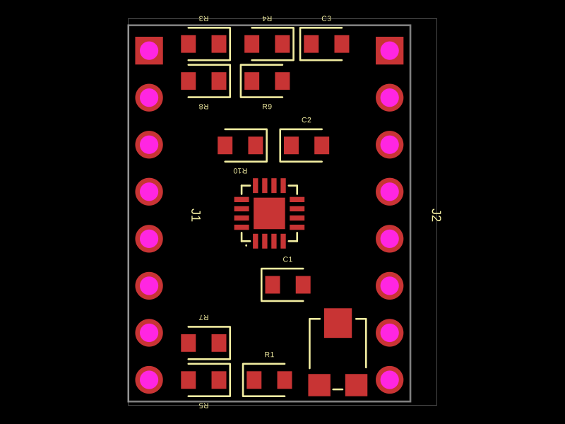 Similar packageAyushjhawar8/stepper-mini-motorThis code defines a schematic and PCB layout for a motor driver IC (TC78H670FTG) with associated passive components, power supply capacitors, resistors, headers, and mechanical footprints, all mapped with specific pin configurations and connections.
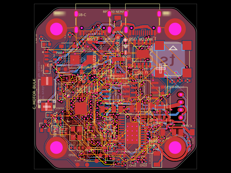 Discover something newimrishabh18/rp2040-motor-controllerA four-layer RP2040-based NEMA17 stepper controller with USB-C power/data, CH224K USB-PD negotiation, DRV8825 dual H-bridge drive, current/temperature telemetry, RGB status LED, buzzer alarm, QSPI flash, and optional AS5600 encoder.