rushabhcodes/usb-audio-dac
A tscircuit package created by rushabhcodes.
- Version
- 1.1.2
- License
- unset
- Stars
- 0
index.circuit.tsx
PCB
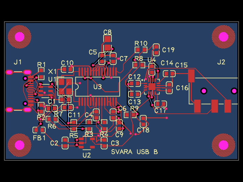
Schematic

import { Fragment } from "react"
import { assembly } from "tscircuit"
import { SnapFitEnclosure, mountingPoints } from "./enclosure"
import { glyphLineAlphabet, glyphAdvanceRatio } from "@tscircuit/alphabet"
import {
  UsbCReceptacle, UsbEsdProtection, UsbDac, Regulator3V3,
  HeadphoneAmplifier, HeadphoneJack, Crystal12MHz, PowerFerriteBead,
  Resistor22Ohm, Resistor1k5, Resistor5k1, Resistor100k, Resistor1M,
  Capacitor100nF, Capacitor1uF, Capacitor2u2, Capacitor10uF, Capacitor33pF,
  Capacitor22nF,
} from "./imports"

const GND = "net.GND"
const VBUS = "net.USB_5V"
const V5 = "net.FILTERED_5V"
const V3 = "net.AMP_3V3"
const DVDD = "net.DAC_DVDD"
const active = "net.USB_ACTIVE"

const referenceStyle = { pcbSx: { "& silkscreentext": { visibility: "hidden" } } } as const
const referenceLabels = [
  ["J1", -24, 6.7],
  ["J2", 23, 6.7],
  ["R1", -18.5, 6.1],
  ["R2", -18.5, -6.1],
  ["U1", -16, 2.7],
  ["C1", -16.15, -2.4],
  ["R3", -7.5, -10],
  ["R4", -4, -10],
  ["R5", -11, -10.3],
  ["FB1", -19, -10.8],
  ["C2", -15.5, -12],
  ["U2", -8, -14.8],
  ["C3", -1.5, -12],
  ["U3", -5.5, 1],
  ["R6", -16, -8.1],
  ["C4", -7.5, -5.5],
  ["C5", -6.6, 9],
  ["C6", 0.2, -4],
  ["C7", 0.5, 7.5],
  ["C8", -3.225, 13.6],
  ["C9", -0.5, -10.1],
  ["X1", -16, 4.5],
  ["R7", -14.5, -5.3],
  ["C10", -12.5, 6.5],
  ["C11", -11, -5.5],
  ["R9", 3, -4],
  ["R10", 4.5, 11],
  ["C18", 5, -9],
  ["C19", 10.8, 9.5],
  ["C12", 3, 3.3],
  ["C13", 3, -2.5],
  ["U4", 7, 7.2],
  ["R8", 4, 7.5],
  ["C14", 10.5, 6.5],
  ["C15", 13.8, 6],
  ["C16", 14, 0.75],
  ["C17", 9, -4.5],
] as const

const dacPosition = { pcbX: -5.5, pcbY: 1, pcbRotation: 0 }
const crystalPosition = { pcbX: -13, pcbY: 1, pcbRotation: 270 }

// One millimetre characters with 0.15 mm ink meet JLCPCB's legend limits.
function SilkLabel({ text, x, y }: { text: string; x: number; y: number }) {
  let advance = 0
  const lines = [...text].flatMap((char) => {
    const offset = advance
    advance += glyphAdvanceRatio[char] ?? 0.7
    return (glyphLineAlphabet[char] ?? []).map((line) => ({
      x1: line.x1 + offset, y1: line.y1, x2: line.x2 + offset, y2: line.y2,
    }))
  })
  const left = Math.min(...lines.flatMap((p) => [p.x1, p.x2]))
  const right = Math.max(...lines.flatMap((p) => [p.x1, p.x2]))
  const bottom = Math.min(...lines.flatMap((p) => [p.y1, p.y2]))
  const top = Math.max(...lines.flatMap((p) => [p.y1, p.y2]))
  const scale = 1 / (top - bottom)
  const point = (px: number, py: number) => ({
    x: x + (px - (left + right) / 2) * scale,
    y: y + (py - (bottom + top) / 2) * scale,
  })
  return <>{lines.map((p, i) => <Fragment key={i}><silkscreenpath strokeWidth={0.15}
    route={[point(p.x1, p.y1), point(p.x2, p.y2)]} /></Fragment>)}</>
}

// tscircuit pcbPath points are relative to the starting component's footprint.
function relativePath(at: typeof dacPosition, points: { x: number; y: number }[]) {
  const angle = -at.pcbRotation * Math.PI / 180
  return points.map(({ x, y }) => ({
    x: (x - at.pcbX) * Math.cos(angle) - (y - at.pcbY) * Math.sin(angle),
    y: (x - at.pcbX) * Math.sin(angle) + (y - at.pcbY) * Math.cos(angle),
  }))
}

/** Svara USB revision B. See README.md for design assumptions and release checks. */
export default function SvaraUsb() {
  return (
    <assembly.device name="SvaraUsb">
    <board name="B1" width="54mm" height="32mm" layers={2} thickness="1.6mm"
      minTraceWidth="0.15mm" autorouter={{ preset: "auto_local", traceClearance: 0.2 }}
      schLayout={{ layoutMode: "none" }}
      minViaHoleDiameter={0.3} minViaPadDiameter={0.6}
      minTraceToHoleEdgeClearance={0.25} minTraceToPadEdgeClearance={0.15} minPadEdgeToPadEdgeClearance={0.15}>
      <schematicsheet name="Svara USB revision B" sheetSize="ANSI_B" sheetWidth={650} sheetHeight={340}>
      <net name="GND" isGroundNet nominalTraceWidth="0.2mm" />
      <net name="USB_5V" isPowerNet nominalTraceWidth="0.15mm" />
      <net name="FILTERED_5V" isPowerNet nominalTraceWidth="0.15mm" />
      <net name="AMP_3V3" isPowerNet nominalTraceWidth="0.2mm" />
      <net name="DAC_DVDD" isPowerNet />
      <net name="DAC_VCCP" isPowerNet />
      <net name="DAC_VCCL" isPowerNet />
      <net name="DAC_VCCR" isPowerNet />

      {/* USB-C USB 2.0 sink: separate Rd resistors, duplicated data contacts. */}
      <UsbCReceptacle {...referenceStyle} name="J1" allowOffBoard pcbX={-23.1} pcbY={0} pcbRotation={270}
        schX={-24} schY={5} schWidth={3} schHeight={7}
        connections={{
          EH1: GND, EH2: GND, EH3: GND, EH4: GND, GND1: GND, GND2: GND,
          VBUS1: VBUS, VBUS2: VBUS, CC1: "net.CC1", CC2: "net.CC2",
          DP1: "net.USB_DP", DP2: "net.USB_DP", DN1: "net.USB_DM", DN2: "net.USB_DM",
        }} />
      <Resistor5k1 {...referenceStyle} name="R1" pcbX={-18.5} pcbY={4} pcbRotation={90} schX={-26} schY={-2}
        connections={{ pin1: "net.CC1", pin2: GND }} />
      <Resistor5k1 {...referenceStyle} name="R2" pcbX={-18.5} pcbY={-4} pcbRotation={90} schX={-22} schY={-2}
        connections={{ pin1: "net.CC2", pin2: GND }} />
      {/* USBLC6: feed-through channels 1/6, 3/4; 2=GND, 5=VBUS. */}
      <UsbEsdProtection {...referenceStyle} name="U1" pcbX={-17.5} pcbY={0} pcbRotation={270}
        schX={-18} schY={5}
        connections={{ pin1: "net.USB_DP", pin6: "net.USB_DP",
          pin3: "net.USB_DM", pin4: "net.USB_DM", pin2: GND, pin5: VBUS }} />
      <Capacitor100nF {...referenceStyle} name="C1" pcbX={-16.15} pcbY={-4}
        schX={-18} schY={1} schRotation={270}
        connections={{ pin1: VBUS, pin2: GND }} />
      <Resistor22Ohm {...referenceStyle} name="R3" pcbX={-7.5} pcbY={-8} pcbRotation={90}
        schX={-12} schY={5.5}
        connections={{ pin1: "net.USB_DM", pin2: "net.DAC_DM" }} />
      <Resistor22Ohm {...referenceStyle} name="R4" pcbX={-4} pcbY={-8} pcbRotation={90}
        schX={-12} schY={4}
        connections={{ pin1: "net.USB_DP", pin2: "net.DAC_DP" }} />
      {/* Pull-up on cable side of the series resistor, powered by DAC VDD. */}
      <Resistor1k5 {...referenceStyle} name="R5" pcbX={-11} pcbY={-8} pcbRotation={90}
        schX={-15} schY={8} schRotation={270}
        connections={{ pin1: DVDD, pin2: "net.USB_DP" }} />

      {/* DAC uses internal regulators; LP5907 powers only the amplifier. */}
      <PowerFerriteBead {...referenceStyle} name="FB1" pcbX={-19} pcbY={-9} schX={-24} schY={-8}
        connections={{ pin1: VBUS, pin2: V5 }} />
      <Capacitor1uF {...referenceStyle} name="C2" pcbX={-13} pcbY={-12} pcbRotation={90}
        schX={-21} schY={-10} schRotation={270}
        connections={{ pin1: V5, pin2: GND }} />
      <Regulator3V3 {...referenceStyle} name="U2" pcbX={-8} pcbY={-12} pcbRotation={180}
        schX={-16} schY={-8} schWidth={3}
        connections={{ IN: V5, EN: V5, GND, OUT: V3 }} />
      <Capacitor1uF {...referenceStyle} name="C3" pcbX={-4} pcbY={-12} pcbRotation={90}
        schX={-12} schY={-10} schRotation={270}
        connections={{ pin1: V3, pin2: GND }} />

      {/* PCM2704C bus-powered, 100 mA descriptor, default USB identity.
          Its four 3.3 V output rails are intentionally separate. */}
      <UsbDac {...referenceStyle} name="U3" {...dacPosition}
        schX={0} schY={3} schWidth={5} schHeight={9}
        schPinArrangement={{
          leftSide: [8, 9, 28, 1, 3, 2, 4, 21, 25, 26, 22, 23, 24],
          rightSide: [14, 15, 27, 5, 18], topSide: [10, 7, 20, 13, 16],
          bottomSide: [6, 11, 12, 17, 19],
        }}
        connections={{
          VBUS: V5, VDD: DVDD, VCCP: "net.DAC_VCCP", VCCL: "net.DAC_VCCL",
          VCCR: "net.DAC_VCCR", VCOM: "net.DAC_VCOM",
          DGND: GND, ZGND: GND, AGNDL: GND, AGNDR: GND, PGND: GND,
          D_NEG: "net.DAC_DM", D_POS: "net.DAC_DP", XTI: "net.XTI", XTO: "net.XTO",
          DT: "net.ROM_DATA", PSEL: DVDD, HOST: GND, TEST0: DVDD, TEST1: DVDD,
          HID0: GND, HID1: GND, HID2: GND, N_SSPND: active,
          VOUTL: "net.DAC_L", VOUTR: "net.DAC_R",
        }} />
      <Resistor100k {...referenceStyle} name="R6" pcbX={-16} pcbY={-6.5}
        schX={-7} schY={7} schRotation={270}
        connections={{ pin1: DVDD, pin2: "net.ROM_DATA" }} />
      <Capacitor1uF {...referenceStyle} name="C4" pcbX={-5.825} pcbY={-5.5} pcbRotation={270}
        schX={-6} schY={13} schRotation={270}
        connections={{ pin1: DVDD, pin2: GND }} />
      <Capacitor1uF {...referenceStyle} name="C5" pcbX={-4.525} pcbY={7.5} pcbRotation={90}
        schX={-3} schY={13} schRotation={270}
        connections={{ pin1: "net.DAC_VCCP", pin2: GND }} />
      <Capacitor1uF {...referenceStyle} name="C6" pcbX={-1.925} pcbY={-5.5} pcbRotation={270}
        schX={0} schY={13} schRotation={270}
        connections={{ pin1: "net.DAC_VCCL", pin2: GND }} />
      <Capacitor1uF {...referenceStyle} name="C7" pcbX={-1.925} pcbY={7.5} pcbRotation={90}
        schX={3} schY={13} schRotation={270}
        connections={{ pin1: "net.DAC_VCCR", pin2: GND }} />
      <Capacitor10uF {...referenceStyle} name="C8" pcbX={-3.225} pcbY={11} pcbRotation={90}
        schX={6} schY={13} schRotation={270}
        connections={{ pin1: "net.DAC_VCOM", pin2: GND }} />
      <Capacitor1uF {...referenceStyle} name="C9" pcbX={-0.5} pcbY={-8} pcbRotation={90}
        schX={-9} schY={13} schRotation={270}
        connections={{ pin1: V5, pin2: GND }} />

      {/* CL ≈ 33 pF / 2 + 3.5 pF stray = 20 pF; verify on the prototype. */}
      <Crystal12MHz {...referenceStyle} name="X1" {...crystalPosition}
        schX={-1} schY={-9}
        connections={{ pin1: "net.XTI", pin3: "net.XTO", pin2: GND, pin4: GND }} />
      <Resistor1M {...referenceStyle} name="R7" pcbX={-13} pcbY={-2}
        schX={-1} schY={-6}
        connections={{ pin1: "net.XTI", pin2: "net.XTO" }} />
      <Capacitor33pF {...referenceStyle} name="C10" pcbX={-12.5} pcbY={5}
        schX={-5} schY={-11} schRotation={270}
        connections={{ pin1: "net.XTI", pin2: GND }} />
      <Capacitor33pF {...referenceStyle} name="C11" pcbX={-12.5} pcbY={-3.8}
        schX={3} schY={-11} schRotation={270}
        connections={{ pin1: "net.XTO", pin2: GND }} />

      {/* Keep all oscillator branches on the top layer. */}
      <trace name="CLK_IN" from="U3.XTI" to="X1.pin1" width={0.15}
        pcbPath={relativePath(dacPosition, [{ x: -9.725036, y: 4.455162 }, { x: -11, y: 4.455162 },
          { x: -11, y: 3.6 }, { x: -13.850011, y: 3.6 }, { x: -13.850011, y: 2.100074 }])} />
      <trace name="CLK_OUT" from="U3.XTO" to="X1.pin3" width={0.15}
        pcbPath={relativePath(dacPosition, [{ x: -9.725036, y: -2.455162 }, { x: -11, y: -2.455162 },
          { x: -11, y: -0.100074 }, { x: -12.149989, y: -0.100074 }])} />
      <trace name="CLK_LOAD_IN" from="X1.pin1" to="C10.pin1" width={0.15}
        pcbPath={relativePath(crystalPosition, [{ x: -13.850011, y: 2.100074 }, { x: -14.8, y: 3.05 },
          { x: -14.8, y: 5 }, { x: -13.200024, y: 5 }])} />
      <trace name="CLK_LOAD_OUT" from="X1.pin3" to="C11.pin1" width={0.15}
        pcbPath={relativePath(crystalPosition, [{ x: -12.149989, y: -0.100074 }, { x: -12.149989, y: -2.8 }, { x: -13.200024, y: -3.8 }])} />
      <trace name="CLK_BIAS_IN" from="X1.pin1" to="R7.pin1" width={0.15}
        pcbPath={relativePath(crystalPosition, [{ x: -13.850011, y: 2.100074 }, { x: -15.2, y: 2.100074 }, { x: -15.2, y: -2 }, { x: -13.7, y: -2 }])} />
      <trace name="CLK_BIAS_OUT" from="X1.pin3" to="R7.pin2" width={0.15}
        pcbPath={relativePath(crystalPosition, [{ x: -12.149989, y: -0.100074 }, { x: -12.149989, y: -2 }, { x: -12.3, y: -2 }])} />

      {/* 22 ohm/22 nF RF filters, then AC coupling (fc ≈ 8 Hz at 0 dB gain).
          DirectPath outputs need no output coupling capacitors. */}
      <Resistor22Ohm {...referenceStyle} name="R9" pcbX={2} pcbY={-5.5}
        schX={8} schY={7}
        connections={{ pin1: "net.DAC_L", pin2: "net.FILTER_L" }} />
      <Resistor22Ohm {...referenceStyle} name="R10" pcbX={4.5} pcbY={9.5}
        schX={8} schY={4}
        connections={{ pin1: "net.DAC_R", pin2: "net.FILTER_R" }} />
      <Capacitor22nF {...referenceStyle} name="C18" pcbX={5} pcbY={-7} pcbRotation={90}
        schX={10} schY={5.5} schRotation={270}
        connections={{ pin1: "net.FILTER_L", pin2: GND }} />
      <Capacitor22nF {...referenceStyle} name="C19" pcbX={8} pcbY={9.5} pcbRotation={90}
        schX={10} schY={2.5} schRotation={270}
        connections={{ pin1: "net.FILTER_R", pin2: GND }} />
      <Capacitor1uF {...referenceStyle} name="C12" pcbX={3} pcbY={1.75}
        schX={12} schY={7}
        connections={{ pin1: "net.FILTER_L", pin2: "net.AMP_INL" }} />
      <Capacitor1uF {...referenceStyle} name="C13" pcbX={3} pcbY={-0.75}
        schX={12} schY={4}
        connections={{ pin1: "net.FILTER_R", pin2: "net.AMP_INR" }} />
      <HeadphoneAmplifier {...referenceStyle} name="U4" pcbX={7} pcbY={1}
        schX={19} schY={3} schWidth={4} schHeight={6}
        schPinArrangement={{ leftSide: [1, 4, 2, 3, 13, 6, 7],
          rightSide: [16, 5, 11, 9, 8, 12], topSide: [14], bottomSide: [15, 10, 17] }}
        connections={{
          INL_NEG: "net.AMP_INL", INR_NEG: "net.AMP_INR", INL_POS: GND, INR_POS: GND,
          VDD: V3, EN: active, G0: V3, G1: GND, // G0=1, G1=0: 0 dB.
          SGND: GND, PGND: GND, EP: GND, CPP: "net.CP_POS", CPN: "net.CP_NEG",
          HPVDD: "net.HPVDD", HPVSS: "net.HPVSS", OUTL: "net.HP_L", OUTR: "net.HP_R",
        }} />
      <Resistor100k {...referenceStyle} name="R8" pcbX={4} pcbY={6}
        schX={12} schY={-1} schRotation={270}
        connections={{ pin1: active, pin2: GND }} />
      <Capacitor2u2 {...referenceStyle} name="C14" pcbX={7} pcbY={5} pcbRotation={90}
        schX={13} schY={12} schRotation={270}
        connections={{ pin1: V3, pin2: GND }} />
      {/* HPVDD is internally generated. Never connect to AMP_3V3. */}
      <Capacitor2u2 {...referenceStyle} name="C15" pcbX={11} pcbY={4}
        schX={26} schY={-5} schRotation={270}
        connections={{ pin1: "net.HPVDD", pin2: GND }} />
      <Capacitor1uF {...referenceStyle} name="C16" pcbX={11} pcbY={0.75} pcbRotation={90}
        schX={22} schY={-5}
        connections={{ pin1: "net.CP_NEG", pin2: "net.CP_POS" }} />
      <Capacitor1uF {...referenceStyle} name="C17" pcbX={9} pcbY={-3}
        schX={18} schY={-5} schRotation={270}
        connections={{ pin1: "net.HPVSS", pin2: GND }} />
      {/* PJ-320D: 2=tip L, 3=ring R, 4=second ring, 1=sleeve.
          Ground both return contacts for TRS headphones; no microphone input. */}
      <HeadphoneJack {...referenceStyle} name="J2" allowOffBoard pcbX={20.9} pcbY={0} pcbRotation={180}
        schX={29} schY={5}
        connections={{ pin2: "net.HP_L", pin3: "net.HP_R", pin1: GND, pin4: GND }} />

      {mountingPoints.map(([x, y], i) => <Fragment key={`mount-${i}`}>
        <hole name={`H${i + 1}`} pcbX={x} pcbY={y} diameter={2.2} />
        <keepout shape="circle" pcbX={x} pcbY={y} radius={2.7} layers={["top", "bottom"]} />
      </Fragment>)}

      <copperpour layer="bottom" connectsTo={GND} clearance={0.25} cutoutMargin={0.3} boardEdgeMargin={0.3} />

      {referenceLabels.map(([name, x, y]) => (
        <Fragment key={name}><SilkLabel text={name} x={x} y={y} /></Fragment>
      ))}
      <SilkLabel text="SVARA USB B" x={3} y={-14} />
      <schematictext text="USB-C / ESD / full-speed interface" schX={-20} schY={12} fontSize={0.6} />
      <schematictext text="Filtered USB power / amplifier LDO" schX={-19} schY={-5} fontSize={0.6} />
      <schematictext text="PCM2704C / 16-bit stereo / 48 kHz max" schX={0} schY={17} fontSize={0.6} />
      <schematictext text="12 MHz crystal" schX={0} schY={-4} fontSize={0.6} />
      <schematictext text="TPA6132A2 / 0 dB / ground-referenced output" schX={21} schY={16} fontSize={0.6} />
      </schematicsheet>
    </board>
    <SnapFitEnclosure />
    </assembly.device>
  )
}
Related Packages
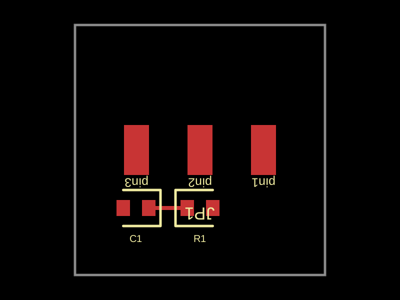 More from this authorrushabhcodes/ttThis code models a 10mm by 10mm PCB with a 1kΩ resistor and a 1000pF capacitor connected via a trace.
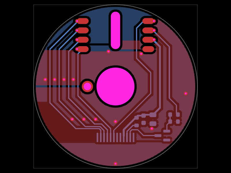 Discover something newhrithik18k/smartknob-screenA mixed SMT component library containing 3.3V regulators, resistors/capacitors, MOSFETs/transistors, USB-UART and sensor ICs, LEDs, connectors, an inductor, and related PCB footprints/CAD models.