rushabhcodes/desk-fidget-counter
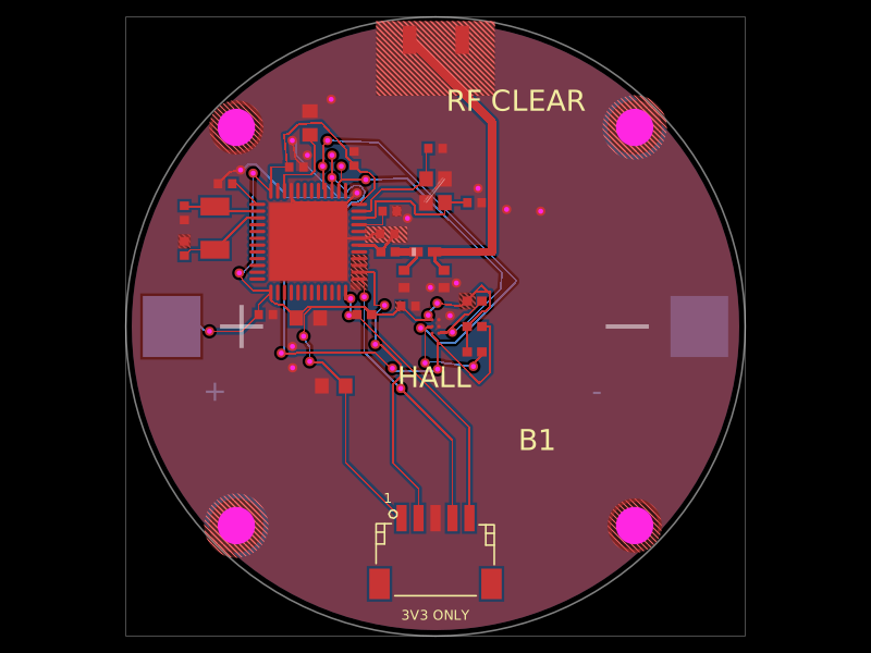
A desk knob assembly combining a circuit board with PETG-printed mechanical parts and vendor CAD-modeled hardware.
- Version
- 5.6.1
- License
- MIT
- Stars
- 0
validation/REPORT.md
# Repository readiness / v5.6.0

Reviewed **7 November 2026**. **Local design checks pass; full fabrication clearance remains conditional on JLCPCB accepting the short USB plated slots.** Native routing, source/footprint checks, independent export DRC and mechanical checks pass. Physical operation and manufacturing tolerances remain first-prototype tests. The E5 enclosure has six printed parts and four screws, reduced from eight prints and fourteen screws. The grip includes its optical track, and two screen screws retain both carrier and bezel. Physical bearing retention and printed fit still require the coupon and prototype checks. This source revision is prepared for publication on GitHub and TSCircuit. No new fabrication kit, release archive, supplier upload or order is created; you will export/download fabrication files and order later.

**Do not order v5.4.0.** That historical release has an undersized U3 FRAM footprint and outdated assembly angles. Its generated manufacturing outputs and manifest were removed from the working revision. Old reports or hashes do not validate a new export. Use the current source and freshly export a complete consistent set when ordering.

## Verified source and copper

| Check | Result |
|---|---|
| TypeScript, netlist and schematic placement | Pass |
| PCB placement | Pass; zero errors and zero warnings |
| Design contract | 39 references, 38 fitted, all top; two copper layers, 1.6 mm board |
| Exact JLCPCB footprints | 23 unchanged imports; 39 references and 173 copper pads verified |
| Native routing | 118 traces, 136 vias; zero circuit error records |
| Gerber-derived shorts | No shorts on either copper layer |
| Independent KiCad 10.0.7 DRC | Zero violations and zero unconnected items; errors and warnings included |
| Export preservation | All 173 physical pad centres and plated drills match source; every native trace/via unchanged after finalization |
| Assembly CAD | 22 named mechanical parts; 38 fitted package models; same PCB geometry in bare/assembly entrypoints |
| Mechanical fit | Six watertight product prints; full rotor sweep, package/screen/wire clearance, USB/button access and four bearing-race contacts pass under stated assumptions |
| Firmware/companion | Software tests and linked ARM image checks pass; unchanged firmware 5.0.0, 61,344-byte image |

The machine-readable [readiness record](readiness.json) fingerprints the validated source and evidence. The [KiCad report](kicad-drc.json), [zone-refill record](pour-cleanup.json), [mechanical geometry checks](../mechanical/geometry-check.json) and [assembly checks](../mechanical/cad/assembly-check.json) hold the underlying results. The E5 CAD update retains the checked E3 PCB geometry and native routing. Current local recheck logs are recorded with the `e5-` prefix; prior `v550-*` copper reports refer to this unchanged board.

All purchased PCB footprints use byte-for-byte exact `tsci import --jlcpcb --use-exact-footprint` files in `imports/jlc`, with [hashes/catalogue IDs](../reference/jlcpcb-footprints.json). Logical aliases retain physical pin numbers. The project adapters account for library zero angles and top-entry metadata without replacing copper, drills, mask or courtyards. Unprintable body silkscreen is omitted for J1/J4/J6/SW1 and one outline in each closely spaced resistor pair; J4 has a separate pin-1 mark. Display labels sit left of J6.

U3 now uses the real narrow SOP8 MB85RC256VPNF-G-AMERE2 footprint, C45273903. Its lands are checked against the RAMXEED datasheet's 6.00±0.20 mm lead span and maximum lead width. J4 is genuine JST C131342, with six imported Ø0.9000236 mm drills. The DNP J6 C5156616 footprint provides eight Ø0.999998 mm solder holes; do not buy/install its header. Use the cable supplied with Waveshare 19192.

## Routing rules and remaining style warning

The built-in `auto_local` Pipeline 7 runs two phases at 2x effort: 14 local MCU decoupling/bulk branches, then the remaining board. Component positions and the original large window are retained. Every trace/via is native output; there is no custom router, manual copper, coordinate repair, saved-path replay or external routing engine.

Both phases request 0.15 mm tracks. The solver produces ordinary legal neck-downs to **0.115710653 mm**, above the manufacturer's documented 0.10 mm limit; most segments are 0.15 mm. Four explicitly requested local MCU bypass/return branches remain ≥0.15 mm, including VSSA→C8. The 4 mm local decoupling length constraint remains enforced. The reported VSSA thin-trace warning is resolved.

[Fabrication rules](../reference/fabrication-rules.json) record the [manufacturer's capabilities](https://jlcpcb.com/capabilities/pcb-capabilities/): track/via copper gap ≥0.10 mm; component pad spacing ≥0.15 mm; via Ø0.30/0.60 mm drill/pad; via drill-edge spacing ≥0.20 mm; component PTH drill-edge spacing ≥0.45 mm; PTH drill-to-copper ≥0.28 mm; NPTH-to-copper ≥0.20 mm; board-edge copper ≥0.30 mm. The earlier blanket 0.15 mm track-gap assumption was more conservative than that published process and is not used as a manufacturer limit.

One native **cosmetic** warning remains: ENC_B has a 5.06 mm bottom segment at 186.10°, 6.10° from the preferred 180° direction. This passes clearance/connectivity and has not been manually straightened.

## Independent check and reproduction

Pinned toolchain: tscircuit 0.0.3077, core 0.0.2267, capacity-autorouter 0.0.1038, Bun 1.3.3, TypeScript 5.9.3; independent DRC uses KiCad 10.0.7.

Run the commands in [manufacturing guidance](../manufacturing/README.md). The independent `--check-only` export writes temporary evidence under `/tmp`, without producing an order kit. It applies the declared rules, refills the ground pours and permits removal only of isolated ground fragments. This final check removed **zero** ground zones. Native traces and vias are required to match the raw export exactly; none were changed. There are no per-violation DRC exclusions.

KiCad's default informational ignored checks are listed in its report: missing courtyard, off-centre track/via endpoint, tuning geometry, schematic footprint filters and footprint-type classification. No electrical clearance, short, drill or connectivity violation is suppressed. Supplier footprint geometry is additionally verified directly against its unmodified imports.

CAD uses included relative asset paths and regenerated source-bound hashes. It does not depend on an unpublished remote tag. Bare PCB and full assembly circuit JSON have identical manufactured PCB records. The cap sweep is checked at 13 positions from 0 to 0.6 mm, with fingertip clearance, fixed switch-housing clearance and side-ear stop engagement. These nominal checks do not certify printed friction or safe switch overtravel. The assembled and exploded models include the fixed screen, original display plug, eight wires, fasteners, one complete bearing object and soft capture pads.

## Open manufacturer process review: USB shield slots

The exact J1/C165948 import contains two approximately **0.80×1.20 mm** and two **0.80×1.50 mm** plated slots: length/width ratios **1.5** and **1.875**. JLCPCB's [capabilities](https://jlcpcb.com/capabilities/pcb-capabilities/) and [ordering instructions](https://jlcpcb.com/help/article/instructions-for-ordering) say slot length should be at least twice its width. Generic KiCad clearance/connectivity DRC does not check that ratio.

JLCPCB [also describes drilling short plated slots](https://jlcpcb.com/blog/reliable-pcb-slot-holes-design), and lists this exact USB component, but neither establishes process acceptance of this particular board. **Obtain JLCPCB's specific DFM/process acceptance of these original slot dimensions and finished-hole tolerances before fabrication**, or qualify another connector and rerun routing/mechanical/export checks. The exact supplier footprint has not been silently altered to hide the issue. [Measured slots and review status](supplier-review.json). No supplier contact, new upload or approval was performed in this task.

## Supplier handoff and physical limits

The historical signed-in v5.4.0 upload matched 22/22 BOM lines and 38 top placements, but it exposed the old footprint/angle defects and was not approved for ordering. The old $190.15 quote for five bare/two assembled boards excludes India shipping/import charges and does not price this corrected geometry. [Stock/cost evidence](../reference/jlcpcb-cost-review.json) is a point-in-time record, not reserved stock. No replacement upload, current price or final JLC feeder/origin approval is claimed.

When you export later, recheck exact part availability and the BOM/CPL preview against real copper and physical pin 1. Keep all 38 fitted parts on top and J6 DNP. Supplier engineering DFM approval and final assembly feeder/origin confirmation remain part of your future order, as with any prototype.

Physical USB operation, power/suspend behaviour, optical counts, actual printed fit, supplied-wire dressing, bearing race contact and tactile access remain unmeasured. The bearing's 60×75×7 mm boundary is published; internal/race details and unpublished cable dimensions use the accepted approximations. [BRINGUP.md](BRINGUP.md) and [FIT.md](../mechanical/FIT.md) specify first-build checks. The circular body remains Ø84.8×22.3 mm; the front cap brings overall depth to 88.0 mm. Calibrate/finish the bearing fits to the documented targets; a generic FDM service tolerance is insufficient by itself.

GitHub Actions for commit `72e4b85` could not start because GitHub reported an account billing lock. Local results are recorded separately; no hosted CI pass is claimed.
Related Packages
 More from this authorrushabhcodes/fidget-counter
 Discover something newDevesh36/orbit-turntableORBIT is a USB-C-powered display turntable for photographing jewellery, models and small products. Four-layer ESP32-C3 / ULN2003 PCB, geared stepper, OLED, push encoder, home switch and buzzer, with an enclosed and exploded assembly. Hardware prototype; firmware and physical qualification remain separate.