rushabhcodes/desk-fidget-counter
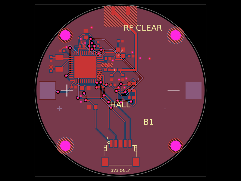
A desk knob assembly combining a circuit board with PETG-printed mechanical parts and vendor CAD-modeled hardware.
- Version
- 5.6.1
- License
- MIT
- Stars
- 0
scripts/export-fabrication.py
#!/usr/bin/env python3
"""SPDX-License-Identifier: MIT. Finalize a source-derived KiCad export with declared fab rules.
Requires KiCad 10 Python (pcbnew) and kicad-cli. No DRC exclusions are set.
"""
from pathlib import Path
import argparse, csv, json, subprocess, sys, tempfile
import pcbnew
ROOT=Path(__file__).resolve().parents[1]
parser=argparse.ArgumentParser(description=__doc__)
parser.add_argument('input_board',type=Path)
parser.add_argument('--check-only',action='store_true',help='Validate in a temporary directory without writing manufacturing outputs')
args=parser.parse_args()
OUT=Path(tempfile.mkdtemp(prefix='desk-fab-check-')) if args.check_only else ROOT/'manufacturing'
REPORT=OUT if args.check_only else ROOT/'validation'
OUT.mkdir(exist_ok=True)
raw=args.input_board
boardpath=OUT/'desk-knob-reve3.kicad_pcb'
b=pcbnew.LoadBoard(str(raw))
def routed_copper(board):
    return sorted((type(t).__name__,t.GetNetname(),t.GetLayer(),
      tuple(t.GetWidth(layer) for layer in (pcbnew.F_Cu,pcbnew.B_Cu)) if isinstance(t,pcbnew.PCB_VIA) else (t.GetWidth(),),
      t.GetStart().x,t.GetStart().y,t.GetEnd().x,t.GetEnd().y,
      t.GetDrillValue() if isinstance(t,pcbnew.PCB_VIA) else 0)
      for t in board.GetTracks())
native_routes=routed_copper(b)
# Keep boards alive while pcbnew's footprint/zone proxy objects are in scope.
loaded_boards=[b]
source=json.loads((ROOT/'dist/index/circuit.json').read_text())
expected={c['name'] for c in source if c['type']=='source_component'}
assert {f.GetReference() for f in b.GetFootprints() if f.GetReference()}==expected, 'Raw KiCad export is stale; export the current circuit JSON first'
source_names={c['source_component_id']:c['name'] for c in source if c['type']=='source_component'}
pcb_components={c['pcb_component_id']:c for c in source if c['type']=='pcb_component'}
source_ports={c['source_port_id']:c for c in source if c['type']=='source_port'}
pcb_ports={c['pcb_port_id']:c for c in source if c['type']=='pcb_port'}
expected_pads={}
for p in [c for c in source if c['type'] in ['pcb_smtpad','pcb_plated_hole']]:
 port=pcb_ports[p['pcb_port_id']];sp=source_ports[port['source_port_id']]
 ref=source_names[pcb_components[p['pcb_component_id']]['source_component_id']]
 expected_pads[ref,str(sp['pin_number'])]=(port,p)
checked=set()
for fp in b.GetFootprints():
 for p in fp.Pads():
  if not p.GetNumber():continue
  key=(fp.GetReference(),p.GetNumber());port,physical=expected_pads[key]
  assert abs(pcbnew.ToMM(p.GetPosition().x)-(100+port['x']))<.0002, f'{key} copper X differs from source'
  assert abs(pcbnew.ToMM(p.GetPosition().y)-(100-port['y']))<.0002, f'{key} copper Y differs from source'
  if physical['type']=='pcb_plated_hole':
   w=physical.get('hole_diameter',physical.get('hole_width'))
   h=physical.get('hole_diameter',physical.get('hole_height'))
   for actual,wanted in zip(sorted([pcbnew.ToMM(p.GetDrillSize().x),pcbnew.ToMM(p.GetDrillSize().y)]),sorted([w,h])):
    assert abs(actual-wanted)<.0002, f'{key} finished drill differs from source'
  checked.add(key)
assert checked==set(expected_pads), 'Raw KiCad export does not contain every source copper pad'
# Preserve the source's optional-component population flag in KiCad.
dnp={c['source_component_id'] for c in source if c['type']=='pcb_component' and c.get('do_not_place')}
dnp_refs={c['name'] for c in source if c['type']=='source_component' and c['source_component_id'] in dnp}
for fp in b.GetFootprints():
 if fp.GetReference() in dnp_refs:fp.SetDNP(True)
# All coordinates and nets come from tscircuit; refill removes floating copper islands.
for priority,z in enumerate(b.Zones(),1):
    if z.GetIsRuleArea():
        assert all(c.get('allow_placements') for c in source if c['type']=='pcb_keepout'), 'Keepout placement flags need individual mapping'
        # Match allowPlacements in the source; housings span the routed window
        # and the connector surrounds its locating holes. Copper stays blocked.
        z.SetDoNotAllowFootprints(False)
        z.SetDoNotAllowPads(False)
        continue
    assert z.GetNetname()=='GND', 'Only the declared ground pours are expected'
    # Native pour fragments can touch/overlap on tessellated boundaries. Distinct
    # priorities let KiCad refill their common ground without ambiguous overlaps.
    z.SetAssignedPriority(priority)
    z.SetIslandRemovalMode(pcbnew.ISLAND_REMOVAL_MODE_ALWAYS)
    z.SetLocalClearance(pcbnew.FromMM(.25))
# Export the actual standalone footprints so library comparison is meaningful.
lib=OUT/'tscircuit.pretty'
lib.mkdir(exist_ok=True)
for old in lib.glob('*.kicad_mod'):old.unlink()
for fp in b.GetFootprints():
    item=fp.GetFPID()
    item.SetLibItemName(pcbnew.UTF8(str(item.GetLibItemName())+'__'+fp.GetReference()))
    fp.SetFPID(item)
    pcbnew.PCB_IO_MGR.FindPlugin(pcbnew.PCB_IO_MGR.KICAD_SEXP).FootprintSave(str(lib),fp)
(OUT/'fp-lib-table').write_text('(fp_lib_table (lib (name "tscircuit")(type "KiCad")(uri "${KIPRJMOD}/tscircuit.pretty")(options "")(descr "Generated from the tscircuit source")))\n')
project={
 'board':{'design_settings':{'rules':{
  'min_clearance':.1,'min_track_width':.1,'min_via_diameter':.6,
  'min_through_hole_diameter':.3,'min_hole_clearance':.2,'min_hole_to_hole':.2,
  'min_copper_edge_clearance':.3,'min_text_height':1.0,'min_text_thickness':.15,'min_silk_clearance':.15}}},
 'net_settings':{'classes':[{'name':'Default','clearance':.1,'track_width':.15,
  'via_diameter':.6,'via_drill':.3,'microvia_diameter':.3,'microvia_drill':.1,
  'diff_pair_width':.15,'diff_pair_gap':.15,'diff_pair_via_gap':.15,'bus_width':12,
  'line_style':0,'pcb_color':'rgba(0, 0, 0, 0.000)','schematic_color':'rgba(0, 0, 0, 0.000)','wire_width':6}]}}
pcbnew.SaveBoard(str(boardpath),b)
boardpath.with_suffix('.kicad_pro').write_text(json.dumps(project,indent=2)+'\n')
# Published JLCPCB 1oz/two-layer rules, checked 2026-11-06. Component
# pad-to-pad and PTH drilling constraints remain stricter than track spacing.
boardpath.with_suffix('.kicad_dru').write_text('''(version 1)
(rule "Component pad clearance"
 (condition "A.Type == 'Pad' && B.Type == 'Pad'")
 (constraint clearance (min 0.15mm)))
(rule "Component plated hole spacing"
 (condition "A.Pad_Type == 'Through-hole' && B.Pad_Type == 'Through-hole'")
 (constraint hole_to_hole (min 0.45mm)))
(rule "Component plated drill to copper"
 (condition "A.Pad_Type == 'Through-hole' || B.Pad_Type == 'Through-hole'")
 (constraint hole_clearance (min 0.28mm)))
''')
# Remove only entire GND zones that KiCad identifies as electrically isolated.
# Native pour fragments can be isolated zones rather than islands of one zone;
# normal island removal alone does not eliminate these zone objects.
removed=[]
for attempt in range(3):
 boardpath.with_suffix('.kicad_pro').write_text(json.dumps(project,indent=2)+'\n')
 result=subprocess.run(['kicad-cli','pcb','drc',str(boardpath),'--refill-zones','--save-board',
  '--format','json','--output',str(REPORT/'kicad-drc.json'),'--exit-code-violations'])
 r=json.loads((REPORT/'kicad-drc.json').read_text())
 isolated={item['uuid'] for v in r['violations'] if v['type']=='isolated_copper' for item in v['items']}
 if not isolated:break
 b=pcbnew.LoadBoard(str(boardpath));loaded_boards.append(b);count=0
 for zone in list(b.Zones()):
  if zone.m_Uuid.AsString() in isolated:
   assert zone.GetNetname()=='GND','Only isolated ground fragments may be removed'
   removed.append({'zone_uuid':zone.m_Uuid.AsString(),'net':'GND','reason':'KiCad isolated_copper'})
   zone.thisown=False
   b.Remove(zone);count+=1
 assert count==len(isolated),'Cannot identify an isolated pour fragment'
 pcbnew.SaveBoard(str(boardpath),b)
(REPORT/'pour-cleanup.json').write_text(json.dumps({'removed_isolated_ground_zones':removed},indent=2)+'\n')
assert not r['violations'] and not r['unconnected_items'], 'DRC is not clean'
final_board=pcbnew.LoadBoard(str(boardpath));loaded_boards.append(final_board)
assert routed_copper(final_board)==native_routes, 'Fabrication export must not change any native trace or via'
if args.check_only:
 print(f'Independent fabrication check passed; native traces/vias unchanged. Temporary evidence: {OUT}')
 sys.exit(0)
gerbers=OUT/'gerbers';gerbers.mkdir(exist_ok=True)
for old in gerbers.glob('desk-knob-*'):old.unlink()
subprocess.run(['kicad-cli','pcb','export','gerbers',str(boardpath),'--output',str(gerbers)+'/',
 '--layers','F.Cu,B.Cu,F.Mask,B.Mask,F.Paste,B.Paste,F.Silkscreen,B.Silkscreen,Edge.Cuts',
 '--subtract-soldermask','--check-zones'],check=True)
subprocess.run(['kicad-cli','pcb','export','drill',str(boardpath),'--output',str(gerbers)+'/',
 '--format','excellon','--excellon-separate-th','--excellon-oval-format','route','--generate-map','--map-format','svg'],check=True)
subprocess.run(['kicad-cli','pcb','export','pos',str(boardpath),'--output',str(OUT/'pick-and-place.csv'),
 '--format','csv','--units','mm','--side','both','--exclude-dnp'],check=True)

# Mechanical pad-only footprints have no reference and must not become placements.
position_file=OUT/'pick-and-place.csv'
with position_file.open(newline='') as f:
    rows=list(csv.DictReader(f))
fields=list(rows[0]); rows=[r for r in rows if r['Ref']]
with position_file.open('w',newline='') as f:
    writer=csv.DictWriter(f,fieldnames=fields);writer.writeheader();writer.writerows(rows)
assert {r['Ref'] for r in rows}==expected-dnp_refs, 'Placement population differs from the source BOM'

# Normalize generator whitespace without changing plotted geometry.
for svg in gerbers.glob('*.svg'):
    svg.write_text('\n'.join(line.rstrip() for line in svg.read_text().splitlines())+'\n')
Related Packages
 More from this authorrushabhcodes/fidget-counter
 Discover something newDevesh36/orbit-turntableORBIT is a USB-C-powered display turntable for photographing jewellery, models and small products. Four-layer ESP32-C3 / ULN2003 PCB, geared stepper, OLED, push encoder, home switch and buzzer, with an enclosed and exploded assembly. Hardware prototype; firmware and physical qualification remain separate.