rushabhcodes/desk-fidget-counter
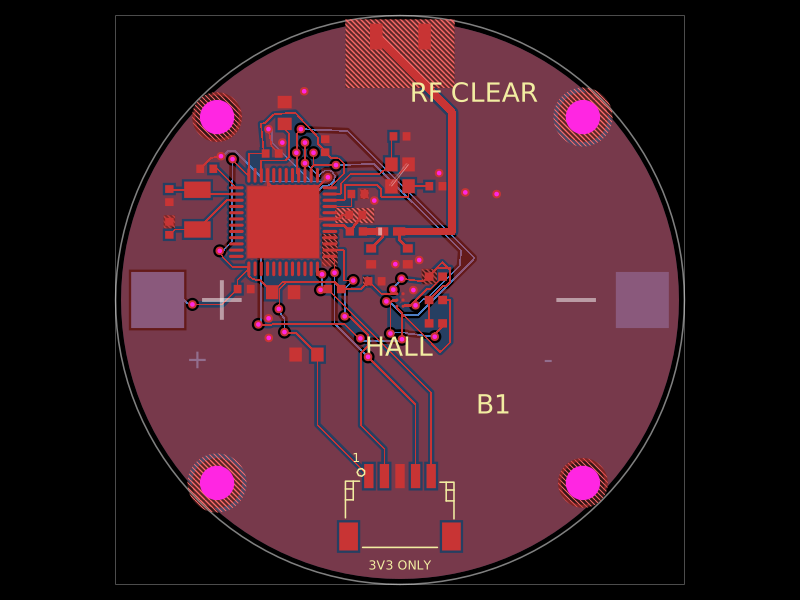
A desk knob assembly combining a circuit board with PETG-printed mechanical parts and vendor CAD-modeled hardware.
- Version
- 5.6.1
- License
- MIT
- Stars
- 0
reference/DATASHEETS.md
# Design evidence and verified package contracts

Reviewed 2026-11-05. Pin numbers in the source are physical package numbers viewed from above. Supplier cache snapshots are saved separately; verify inventory when ordering.

| Item | Primary reference | Contract used |
|---|---|---|
| STM32F072CBT6 | [ST DS9826](https://www.st.com/resource/en/datasheet/stm32f072cb.pdf), Fig. 8 / pin table / LQFP48 package | 7 × 7 mm body, 0.5 mm pitch; 1 VBAT, 7 NRST, 8 VSSA, 9 VDDA, 23/35/47 VSS, 24/48 VDD, 36 VDDIO2. USB PA11/PA12 pins 32/33. SWD PA13/PA14 pins 34/37. I2C1 PB6/7 pins 42/43. BOOT0 pin 44. HSI48 + CRS permits crystal-less USB. Internal D+ pull-up; no external pull-up or series termination required for this MCU. |
| MB85RC256VPNF-G-AMERE2 | [RAMXEED MB85RC256V datasheet](https://www.ramxeed.com/assets/images/products/datasheet/FeRAM/i3/MB85RC256V-DS11v1-E.pdf) | 150 mil SOP8: 3.90×4.90 mm body, 6.00±0.20 mm lead span, 1.27 mm pitch (p.17); **PNF**, not the wider package. Exact C45273903 import uses pad rows 5.364988 mm apart, 1.864995×0.6299962 mm lands; project angle −90° restores the pin-1 top-left orientation. 1/2/3 address, 4 VSS, 5 SDA, 6 SCL, 7 WP, 8 VDD. Addresses grounded → 0x50, WP grounded. 2.7–5.5 V supply. |
| TLV75533PDBVR | [TI TLV755P](https://www.ti.com/lit/ds/symlink/tlv755p.pdf) | SOT23-5 DBV: 1 IN, 2 GND, 3 EN, 4 NC, 5 OUT. 1 uF input, 4.7 uF output ceramic. EN tied to VBUS. |
| USBLC6-2SC6 | [ST DS4260](https://www.st.com/resource/en/datasheet/usblc6-2.pdf) | SOT23-6: data pair 1/6 and 3/4, 2 GND, 5 VBUS. The line-through pads share their respective data net. |
| TYPE-C-31-M-12 | [HRO drawing via LCSC C165948](https://www.lcsc.com/product-detail/usb-connectors_hro-hellen-Type-C-31-M-12_C165948.html) | Original imported copper and drilling retained, including oval shield slots, two 0.6 mm locators, 0.5 mm contact pitch. A6/B6 D+, A7/B7 D−; separate 5.1 kΩ CC1/CC2 Rd; SBU unconnected. All shell tabs grounded. Port faces +Y after 180° rotation. E2 origin is (0,37); the original STEP sets the metal face at Y=42.350 mm and axis Z=5.850 mm. Front body ink overhanging the board is omitted; the mechanical courtyard is retained. |
| Bearing | [Zoty 6712 family](https://www.zotybearing.com/bearings/6700-Series-Ball-Bearings/Factory-direct-selling-thin-wall-ball-bearing-6712-6712RS-6712-2RSsize-60x75x7mm-bearing), [Maysme 6712](https://maysmeprecision.com/Show/?Cid=677) | 6712ZZ, 60 mm ID ×75 mm OD ×7 mm. Select metal shields; verify race contact widths and starting torque on the actual bearing. |

## Rev E3 display, optical encoder and service connectors

| Item | Primary reference | Contract used |
|---|---|---|
| TCUT1600X01 (prototype); _A approved revision | [Vishay 84174, Rev 1.3](https://www.vishay.com/docs/84174/tcut1600x01.pdf), p.6 | 5.5×4×5.7 mm, 3 mm gap, beam 4.5 mm above PCB, two 0.3 mm apertures 0.8 mm apart. Common collector →3V3; each emitter has a 22 kΩ pulldown. IR LED 150 Ω from 3V3 gives about 14 mA at nominal Vf=1.2 V. Library pins 1=A, 2=NC, 3=K, 4=lower E, 5=middle E, 6=C, following the vendor's top-view labels. Numeric IDs are library assignments, not vendor terminal numbers. The lead lands use compact rectangular 0.7 mm-high electrical lands and a 1.0 mm-high NC identification land; optional rounded outer fillet extensions from the proposed vendor pattern are omitted. Inspect the tall sensor's solder joints and mechanical stability. |
| SN74LVC2G17DBVR | [TI SN74LVC2G17](https://www.ti.com/lit/ds/symlink/sn74lvc2g17.pdf) | SOT23-6: 1=1A, 2=GND, 3=2A, 4=2Y, 5=VCC, 6=1Y. Dual noninverting Schmitt conditioner; Y1/Y2 →PB4/PB5 AF1 TIM3_CH1/2. C14 bypasses VCC. |
| Optical geometry | Vishay drawing above; [ST RM0091](https://www.st.com/resource/en/reference_manual/dm00031936-stm32f0x1stm32f0x2stm32f0x8-advanced-armbased-32bit-mcus-stmicroelectronics.pdf), TIM3 encoder mode | Sensor centred at (−23,+10), gap axis radial, rotation 156.501434°. Radius √629=25.0799 mm. 48 periods give 3.283 mm tangential pitch; 0.8 mm channel spacing gives approximately 87.7° phase. 48×4=192 edges/turn; 6 edges/wheel unit gives 32 units/turn. 950 nm opacity, alignment and contrast require actual tests. |
| Waveshare 19192 | [Official resources](https://docs.waveshare.net/1.28inch_LCD_Module/Resources-And-Documents/), [schematic/dimensions](https://www.waveshare.net/w/upload/b/b4/1.28inch_LCD_Module_SchDoc.pdf), [GC9A01A](https://www.waveshare.net/w/upload/5/5e/GC9A01A.pdf) | Non-touch 1.28-inch module, 240×240, active Ø32.4 mm, circular PCB Ø37.5 mm with a 14.28 mm-wide tab giving 40.4 mm overall length. 3.3 V input and logic used, nominal published current 31.2 mA. Physical connector 1 BL, 2 RST, 3 DC, 4 CS, 5 CLK, 6 DIN, 7 GND, 8 VCC. Verify cable continuity. |
| GC9A01 settings | [Waveshare official example archive](https://www.waveshare.net/w/upload/f/fc/LCD_Module_code.zip), RaspberryPi/c/lib/LCD/LCD_1in28.c, 2020-12-16 | `gc9a01-registers.inc` contains transcribed hardware register/value facts, including gamma/power settings. No vendor implementation or font code copied. Own SPI driver, nonblocking startup, original 5×7 glyphs and scanline renderer. RGB565, mode 0, 12 MHz; software CS on PA8, SCK/MOSI on PB13/PB15; MADCTL 0xA8 for the module's left-facing (-X) tab. Validate orientation/colours on hardware. |
| JST PH6 programming | [JST PH drawing](https://www.jst-mfg.com/product/pdf/eng/ePH.pdf) | J4 B6B-PH-K-S, top-entry: pin 1≈(−5,20.5), VREF/SWDIO/SWCLK/NRST/GND/BOOT0. Exact JLCPCB C131342 import: six approximately Ø0.90 mm drills and Ø1.50 mm circular lands. The older Ø0.75 mm drill pattern belongs to the held fabrication files. Display termination J6 is described below; the former board PH8 header is removed. |

# Rev E3 USB-only supply and dashboard

| Item | Primary source | Contract |
|---|---|---|
| TPS22919DCKR / U4 | [TI SLVSEN5B](https://www.ti.com/lit/ds/symlink/tps22919.pdf), DCK SC70-6 | 1 IN=3.3V, 2 GND, 3 ON=PB2, 4 NC, 5 QOD=VOUT, 6 VOUT=PERIPH_3V3; 1.6–5.5V input, 1.5A rating, controlled ramp; external 100k ON pulldown. Not the former BQ24074 footprint. |
| USB cable | [L-com CAU4CC-40M-1M drawing](https://www.l-com.cn/Images/Downloadables/2D/CAU4CC-40M-1M_2D.pdf) | Real 1m C-to-C data cable, 12.9×6.4mm nominal plug cross-section; its general .XX-inch tolerance is ±0.5 mm, so the approach gauge is 13.4×6.9 mm. USB2.0/5V use only. Insertion shoulder, tolerance and strain relief require actual fit verification. |
| Programming harness contacts | [JST PH drawing](https://www.jst-mfg.com/product/pdf/eng/ePH.pdf), pp.1–3 | PHR-6 service housing; SPH-004T-P0.5S accepts 32–28AWG, 0.5–0.9mm insulation. The supplied display cable keeps its original factory PH plug and contacts; no new display crimps are purchased. |
| Screen 3D | [Waveshare original archive](https://files.waveshare.com/upload/4/49/1.28inch_LCD_Module_3D_Drawing.zip) | 0508.stp: 40.453106×37.5×9.2mm bounds. Rigid 180° Y rotation +Z17.75 aligns front Z20.9, carrier back Z17.3 and rear connector bottom Z11.7. No dimensional scaling. |
| Host metrics | [psutil API](https://psutil.readthedocs.io/), [PySerial API](https://pyserial.readthedocs.io/en/latest/pyserial_api.html) | cpu_percent, virtual_memory.percent, sensors_battery; local datetime; USB CDC at 1Hz. Missing battery is -1, stale threshold 5s. Metrics are host-reported, not measured by the knob. |
| Schematic review | [tscircuit handbook](https://github.com/tscircuit/handbook/blob/main/guides/preparing-for-design-review.md) | Descriptive sheet names, readable labels and chip-function/rating annotations using schematictext. |
| USB low power | [ST RM0091](https://www.st.com/resource/en/reference_manual/DM00031936-.pdf), Stop-mode / USB suspend sections and interrupt vector table | USB wake-up is EXTI18 shared with USB IRQ31. Stop exit selects HSI8; firmware restores HSI48 before IRQ processing. TinyUSB's FSDEV driver enters USB FSUSP/LPMODE and clears them on resume. Measure current and wake/reset timing physically. |

VBUS feeds U5 directly; no cell, charging circuit or thermistor remains. C5=1µF on VBUS and C6=4.7µF on 3.3V are the regulator's local ceramic capacitors. U4's C2/C3=1µF bypass input/output. U4 supplies the screen and IR emitter; the MCU/FRAM/Schmitt buffers remain on 3.3V. GPIOs to the LCD are driven low before U4 is disabled, avoiding back-power through unpowered module input protection.

USB configuration requests 100mA, bus-powered. The screen's published nominal current is 31.2mA and the 150Ω IR branch about 14mA; MCU, FRAM and logic add to these. The nominal budget is below 100mA, but maximum active draw, VBUS inrush, regulator temperature and suspended current need measurement. U5's nominal loss is (5−3.3)×load current, e.g. 0.136W at 80mA. No runtime or charge-current claim applies to Rev E3.

The 48-slot ring and sensor locations remain unchanged. LCD carrier and cable are fixed; the manufacturer model and exact specified nominal harness are checked against the rotating swept volume. Supplier models and package solids still omit fine moulding/optical/crimp features; see mechanical/vendor/README.md.

## Rev E3 component audit

Every one of the previous 45 populated references was reviewed; [component-audit.json](component-audit.json) records each decision. The revised board has 38 populated components and an optional DNP header footprint.

| Change | Reason |
|---|---|
| Replace SW1 G12AH with Omron B3U-3000P | Accessible side-actuated front button, opposite USB. The [Omron drawing](https://omronfs.omron.com/en_US/ecb/products/pdf/en-b3u.pdf) gives the footprint and 0.10–0.40 mm pretravel. Short press selects mode; three-second hold clears count. |
| Remove SW2 and R15 | One button handles both actions. NRST remains available through J4. |
| Remove LED1 and R16 | Screen shows mode, storage state and timer faults. |
| Remove R14 | PA0 internal pull-up is explicitly enabled by firmware; the minimum contact current is met. |
| Remove R11 | NRST has an always-present internal 25–55 kΩ pull-up; retain C13 100 nF. See [ST DS9826 NRST characteristics](https://www.st.com/resource/en/datasheet/stm32f072cb.pdf). |
| Remove R29 | Tie VBAT directly to VDD and keep C7 100 nF; no backup cell is used. See [ST AN4080](https://www.st.com/resource/en/application_note/an4080-getting-started-with-stm32f0x1x2x8-hardware-development-stmicroelectronics.pdf). |
| Remove D1 | [USBLC6-2SC6](https://www.st.com/resource/en/datasheet/usblc6-2.pdf) already protects both data lines and VBUS; keep U6 and C1, placed close to USB. |
| C8 →10 nF 0402; add C17 1 µF | Local VDDA bypass and bulk following ST's supply scheme. C8 is [Murata GRM155R71H103KA88D](https://www.farnell.com/datasheets/3973279.pdf), 50 V X7R, 1.0×0.5×0.5 mm nominal; its smaller footprint allows closer placement. |
| C10 →0402; add C18 4.7 µF | Retain 100 nF local VDDIO2 bypass with [Murata GRM155R71C104KA88D](https://www.farnell.com/datasheets/4087776.pdf), 16 V X7R, 1.0×0.5×0.5 mm nominal, and add local bulk. |

U4 and its local capacitors/pulldown remain necessary: the LDO cannot separately disconnect LCD/IR while leaving MCU/FRAM powered during USB suspend. The FRAM, Schmitt conditioner, CC resistors, BOOT0 bias, I²C pull-ups, IR limiter/loads, SPI damping, programming/display connectors and local supply bypass capacitors remain for their documented functions. No external crystal is needed because this MCU uses HSI48/CRS for USB. Firmware 5.0.0 is required for the momentary control and internal pull-up.

## E3 direct button and included cable correction

The board now puts SW1 at (0,−40.9), with the native actuator at Y−42.85 and axis Z4.8. Its original STEP gives a 1.7×1.0 mm actuator face; the front PCB tab and case relief remove the need for a plunger. The B3U datasheet's 0.10–0.40 mm pretravel is retained.

The [Waveshare product package](https://www.waveshare.com/product/1.28inch-lcd-module.htm) explicitly includes a PH2.0 8PIN 20cm cable. Its [photo](https://www.waveshare.com/img/devkit/accessories/PH2.0-wire-20cm-8PIN.jpg) shows eight individual female jumper ends. The former board PH8 header did not accept those sockets. E3 uses the shortened original cable directly at J6; no new harness parts. J6 now uses the exact JLCPCB C5156616 2.54 mm eight-pin header footprint as a solder-pad row, with approximately Ø1.0 mm finished holes. The header is DNP: retain the included display lead and solder only its stripped wires. No extra connector is purchased. Stock wire/terminal dimensions and bend limits are unpublished; CAD cable envelopes remain provisional.

## Mechanics E4 / v5.3.1 approximation basis

The user explicitly requested best approximations where online supplier details could not be found. Maysme 6712ZZ remains the purchased bearing; its 60×75×7 mm boundary is verified. [NSK E1153a](https://www.nsk.com/content/dam/nsk/common/catalogs/ctrgPdf/bearings/e1153a.pdf#page=4) gives the same-size open NB712A mounting analogue (da ≥62, Da ≤73, ra ≤0.3 mm). The E4 race faces, shields, 44 balls and cage are estimates, not NSK or Maysme supplier CAD. Six separate model parts expose their roles and four checked retainer contacts.

[PORON 4701-30 data](https://www.rogerscorp.com/-/media/project/rogerscorp/documents/elastomeric-material-solutions/poron/english/data-sheets/17-006-poron-4701-30-very-soft.pdf) supports grade 320 kg/m³, 1.57 mm thickness and ±10% tolerance for PCB capture pads. Four Ø4 mm and two Ø2.6 mm discs use 0.05 mm 467MP adhesive under the E4 lid. E4 targets calibrated ±0.10 mm fit diameters and ±0.10 mm relative printed heights. [FIT.md](../mechanical/FIT.md) distinguishes the engineering budget from measured process capability.

The supplied LCD lead is retained; E4 models Ø1.2 mm wire and checks Ø1.5 mm. Its 3 mm XZ dressing bend has approximately 1.44 mm minimum 3D centreline radius in the static fan; this is an accepted approximation, not a published wire rating. Electrical parts, pin maps, PCB routing and firmware 5.0.0 are unchanged.

## JLCPCB ordering review — v5.4.0, 6 November 2026

C6/C12/C18 now use **Samsung CL21A475KOFNNNE**, 4.7 µF, 16 V, ±10%, X5R, 0805. [Samsung’s mass-production listing](https://product.samsungsem.com/mlcc/CL21A475KOFNNN.do) gives 2.00×1.25×1.25 mm nominal, each ±0.10 mm. It retains the current nominal package model/land pattern. [LCSC C1746](https://www.lcsc.com/product-detail/C1746.html) verifies catalogue identity. The former [Murata GRM21BR61A475KA73L is obsolete](https://www.digikey.com/en/products/detail/murata-electronics/GRM21BR61A475KA73L/2546893). This is a sourcing change, with unchanged capacitance/footprint and increased voltage rating.

[Exact catalogue mappings](jlcpcb-parts.json) distinguish verified identities from unreserved stock. The exact Vishay U2 and JST J4 codes remain blank rather than using a similar component. [JLCPCB BOM](https://jlcpcb.com/help/article/bill-of-materials-for-pcb-assembly), [CPL](https://jlcpcb.com/help/article/pick-place-file-for-pcb-assembly) and [orientation guidance](https://jlcpcb.com/help/article/pcb-assembly-faqs-part-2) define the upload format and final preview review. [JLC3DP standard FDM tolerances](https://jlc3dp.com/help/article/3d-printing-design-guideline) are looser than the project’s calibrated fit targets; generic printing is not fit-qualified.

## Live JLCPCB sourcing — 6 November 2026

The signed-in upload matched 22 BOM lines / 38 top placements for two assembled boards. Genuine JST B6B-PH-K-S(LF)(SN) is C131342. U2 uses stocked pre-PCN **TCUT1600X01 / C511085** for this prototype; current **TCUT1600X01_A / C24626661** showed zero JLC stock. [Vishay PCN-OPT-1311-2024](https://mm.digikey.com/Volume0/opasdata/d220001/medias/docus/6165/PCN-OPT-1311-2024-REV-0.pdf) changes the phototransistor wafer diameter and explicitly retains characteristics, fit, form and function. This is a wafer revision, not a packaging suffix. The legacy order code is not recommended for a new long-term supply chain; the current _A revision is the documented alternative when stocked. Both use the same physical model, pin functions and land pattern. Application testing remains required.
Related Packages
 More from this authorrushabhcodes/fidget-counter
 Discover something newDevesh36/orbit-turntableORBIT is a USB-C-powered display turntable for photographing jewellery, models and small products. Four-layer ESP32-C3 / ULN2003 PCB, geared stepper, OLED, push encoder, home switch and buzzer, with an enclosed and exploded assembly. Hardware prototype; firmware and physical qualification remain separate.