rushabhcodes/desk-fidget-counter
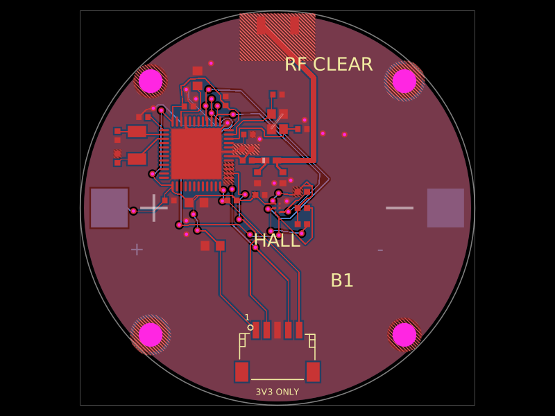
A desk knob assembly combining a circuit board with PETG-printed mechanical parts and vendor CAD-modeled hardware.
- Version
- 5.6.1
- License
- MIT
- Stars
- 0
previews/wiring.svg
<svg xmlns="http://www.w3.org/2000/svg" width="1500" height="1000" viewBox="0 0 1500 1000">
<rect width="1500" height="1000" fill="#f4f7f8"/>
<g font-family="sans-serif" fill="#203943">
<text x="65" y="65" font-size="30">PCB E3 / mechanics E4 — Included display lead</text>
<text x="65" y="105" font-size="20">Keep the original PH display plug; shorten and solder the PCB end. No extra harness parts.</text>
<text x="100" y="175" font-size="22">J6 — solder pads (header DNP)</text>
<text x="960" y="175" font-size="22">Waveshare 19192 — PH2.0</text>
<circle cx="145" cy="230" r="12" fill="#dcbf77" stroke="#203943" stroke-width="3"/>
<text x="180" y="237" font-size="21">1  VCC</text>
<path d="M 350 230 L 1010 230" stroke="#e45555" stroke-width="5"/>
<text x="1040" y="237" font-size="21">8  VCC</text>
<circle cx="145" cy="292" r="12" fill="#dcbf77" stroke="#203943" stroke-width="3"/>
<text x="180" y="299" font-size="21">2  GND</text>
<path d="M 350 292 L 1010 292" stroke="#222c38" stroke-width="5"/>
<text x="1040" y="299" font-size="21">7  GND</text>
<circle cx="145" cy="354" r="12" fill="#dcbf77" stroke="#203943" stroke-width="3"/>
<text x="180" y="361" font-size="21">3  DIN</text>
<path d="M 350 354 L 1010 354" stroke="#59ac70" stroke-width="5"/>
<text x="1040" y="361" font-size="21">6  DIN</text>
<circle cx="145" cy="416" r="12" fill="#dcbf77" stroke="#203943" stroke-width="3"/>
<text x="180" y="423" font-size="21">4  CLK</text>
<path d="M 350 416 L 1010 416" stroke="#528cdd" stroke-width="5"/>
<text x="1040" y="423" font-size="21">5  CLK</text>
<circle cx="145" cy="478" r="12" fill="#dcbf77" stroke="#203943" stroke-width="3"/>
<text x="180" y="485" font-size="21">5  CS</text>
<path d="M 350 478 L 1010 478" stroke="#e4d751" stroke-width="5"/>
<text x="1040" y="485" font-size="21">4  CS</text>
<circle cx="145" cy="540" r="12" fill="#dcbf77" stroke="#203943" stroke-width="3"/>
<text x="180" y="547" font-size="21">6  DC</text>
<path d="M 350 540 L 1010 540" stroke="#ee9b34" stroke-width="5"/>
<text x="1040" y="547" font-size="21">3  DC</text>
<circle cx="145" cy="602" r="12" fill="#dcbf77" stroke="#203943" stroke-width="3"/>
<text x="180" y="609" font-size="21">7  RST</text>
<path d="M 350 602 L 1010 602" stroke="#8a9296" stroke-width="5"/>
<text x="1040" y="609" font-size="21">2  RST</text>
<circle cx="145" cy="664" r="12" fill="#dcbf77" stroke="#203943" stroke-width="3"/>
<text x="180" y="671" font-size="21">8  BL</text>
<path d="M 350 664 L 1010 664" stroke="#b45cce" stroke-width="5"/>
<text x="1040" y="671" font-size="21">1  BL</text>
<text x="65" y="795" font-size="20">J6: X=−21.5 mm; pin 1 Y=4.39 mm, continuing toward −Y at 2.54 mm pitch.</text>
<text x="65" y="835" font-size="20">VCC = switched 3.3V. Check continuity against display labels; factory colours may vary.</text>
<text x="65" y="875" font-size="20">Trial-route before trimming; approx. 37 mm insulated span + 2.55 mm stripped PCB end.</text>
<text x="65" y="915" font-size="20">Best approximation: 1.2 mm wire model, 1.5 mm clearance check; static bends, no flexing in use.</text>
</g></svg>
Related Packages
 More from this authorrushabhcodes/fidget-counter
 Discover something newDevesh36/orbit-turntableORBIT is a USB-C-powered display turntable for photographing jewellery, models and small products. Four-layer ESP32-C3 / ULN2003 PCB, geared stepper, OLED, push encoder, home switch and buzzer, with an enclosed and exploded assembly. Hardware prototype; firmware and physical qualification remain separate.