rushabhcodes/desk-fidget-counter
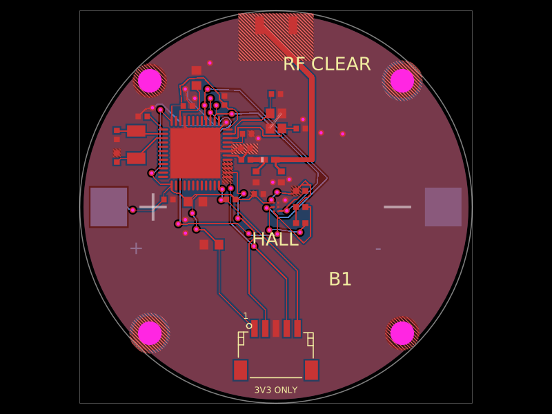
A desk knob assembly combining a circuit board with PETG-printed mechanical parts and vendor CAD-modeled hardware.
- Version
- 5.6.1
- License
- MIT
- Stars
- 0
manufacturing/README.md
# Manufacturing source / PCB E3, mechanics E4

This repository contains the design and its verification record. **No new fabrication kit or release archive is prepared.** Export/download the fabrication files yourself from this validated source when you are ready. Project source is published separately to GitHub and TSCircuit; ordering remains yours to perform.

The obsolete v5.4.0 Gerbers, KiCad board, BOM/CPL, order kit and manifest were removed from this working revision because they contain the undersized U3 FRAM footprint and outdated assembly angles. They remain in Git history and the held old release; do not order them or mix them with new exports. Current part identities and exact supplier footprints live in [the catalogue](../reference/jlcpcb-parts.json), [import provenance](../reference/jlcpcb-footprints.json) and `imports/jlc`.

## Board specification

| Parameter | Requirement |
|---|---|
| Outline | Clipped Ø72 mm body with integral USB/button tabs; 68×83.2 mm total; 34.6×40.6 mm R2 window; four Ø2.7 mm NPTH at (±30, ±15) mm |
| Material | FR-4, 1.6 mm nominal, Tg ≥135°C |
| Copper | Two layers, 1 oz outer copper |
| Finish | ENIG; green solder mask, white silkscreen |
| Track | ≥0.10 mm fabrication limit; native phases request 0.15 mm; actual narrowest neck 0.11571 mm |
| Clearance | ≥0.10 mm track/via copper; ≥0.15 mm component pad-to-pad; ground pour clearance 0.25 mm |
| Routing via | Ø0.30 mm finished drill / Ø0.60 mm pad; generated entirely by the native autorouter |
| Drill spacing | Via drill-edge ≥0.20 mm; component PTH drill-edge ≥0.45 mm |
| Hole-to-copper | NPTH ≥0.20 mm; via drill ≥0.20 mm; component plated drill ≥0.28 mm |
| Copper to edge | ≥0.30 mm; ground pours inset 0.40 mm |
| Assembly | 38 fitted components, all top; J4 genuine JST PH6 included; J6 header DNP |
| Local assembly | Shorten the display's supplied cable and solder its eight ends at J6; trim/inspect underside joints and leads to ≤0.8 mm |

[Fabrication rules](../reference/fabrication-rules.json) record the checked [JLCPCB capabilities](https://jlcpcb.com/capabilities/pcb-capabilities/). Keep 1 oz copper. This is not a controlled-impedance design; USB full-speed signal integrity is a prototype test.

J1 sits at (0,+37) mm; its housing overhangs the supported rear tab so its mouth reaches the shell wall. SW1 remains at (0,−40.9) mm. A captive printed cap operates its original actuator; the lid retains the cap without extra screws. No toggle is installed. J6's pad row is X−21.5 mm, from Y+4.39 downward in 2.54 mm steps: VCC/GND/DIN/CLK/CS/DC/RST/BL. Its labels are to the left of the row. [Wiring and service pin maps](WIRING.md).

## Verification without producing a kit

```sh
bun install --frozen-lockfile
bun run typecheck && bun run test
bun run check:netlist && bun run check:schematic
bun run build
bun run check:placement
bun validation/check-design.mjs
bun run check:footprints && bun run check:shorts && bun run check:assembly
```

For the independent check, install KiCad 10 CLI and its matching Python `pcbnew` module:

```sh
bunx tsci export dist/index/circuit.json -f kicad_pcb -o /tmp/desk-knob-raw.kicad_pcb
/usr/bin/python3 scripts/export-fabrication.py /tmp/desk-knob-raw.kicad_pcb --check-only
```

`--check-only` writes temporary evidence under `/tmp`; it does not produce an order kit. It checks all 173 pad centres and plated drills against source, applies the documented rules, refills ground zones and removes electrically isolated ground fragments. It requires zero DRC violations/unconnected items, no exclusions and an exact match of every native trace and via before/after. It does not route or repair copper. See [validation results](../validation/REPORT.md).

## Open USB slot-process review

J1's exact imported shield slots are 0.8×1.2 mm (two) and 0.8×1.5 mm (two), below the published 2:1 length/width guidance. These require specific JLCPCB DFM/process confirmation before fabrication; a passing KiCad report does not check that ratio. Preserve the supplied geometry while obtaining confirmation, or qualify a replacement connector and rerun checks. [Measured process-review record](../validation/supplier-review.json).

## When you export later

Export all Gerbers, plated/nonplated drills, BOM and placement files from the same freshly built revision. Verify window/outline geometry, exact MPNs, 38 top placements and J6 DNP. Do not reuse the held old CSVs. JLCPCB feeder origins and zero angles still need confirmation against the physical copper and datasheet pin 1 in your final upload preview; a generic 3D model is insufficient.

[JLCPCB guidance](jlcpcb/README.md) records part matching/cost evidence and the remaining supplier steps. The screen, bearing, six prints and final wire/mechanical assembly are separate from PCB assembly. The first prototype still needs [bring-up](../validation/BRINGUP.md) and [fit verification](../mechanical/FIT.md).
Related Packages
 More from this authorrushabhcodes/fidget-counter
 Discover something newDevesh36/orbit-turntableORBIT is a USB-C-powered display turntable for photographing jewellery, models and small products. Four-layer ESP32-C3 / ULN2003 PCB, geared stepper, OLED, push encoder, home switch and buzzer, with an enclosed and exploded assembly. Hardware prototype; firmware and physical qualification remain separate.