rushabhcodes/desk-fidget-counter
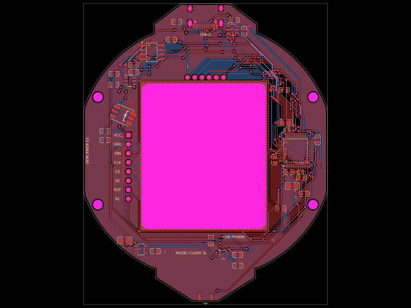
A desk knob assembly combining a circuit board with PETG-printed mechanical parts and vendor CAD-modeled hardware.
- Version
- 5.6.1
- License
- MIT
- Stars
- 0
index.circuit.tsx
PCB
Schematic

import dimensions from "./mechanical/parameters.json"
import fabrication from "./reference/fabrication-rules.json"
import { packageCad } from "./cad"
import { Fragment } from "react"
import { MCU, OpticalSensor, FRAM, mcuPins, JlcChip, JlcConnector, JlcButton, JlcResistor, JlcCapacitor, USB } from "./parts"
import type { PartsEngine } from "@tscircuit/props"
const refStyle={"& silkscreentext":{visibility:"hidden" as const}}
const fixedParts: PartsEngine = {findPart:({sourceComponent})=>sourceComponent.type==="source_component"?sourceComponent.supplier_part_numbers??{}:{}}
const resistorMpns: Record<string,string>={"5.1k":"RC0603FR-075K1L","4.42k":"RC0603FR-074K42L","3.09k":"RC0603FR-073K09L","30k":"RC0603FR-0730KL","100k":"RC0603FR-07100KL","10k":"RC0603FR-0710KL","4.7k":"RC0603FR-074K7L","1k":"RC0603FR-071KL","1M":"RC0603FR-071ML","470k":"RC0603FR-07470KL","150":"RC0603FR-07150RL","22k":"RC0603FR-0722KL","22":"RC0603FR-0722RL"}
const capacitorMpns: Record<string,string>={"100nF":"GRM188R71C104KA01D","1uF":"GRM188R61A105KA61D","4.7uF":"CL21A475KOFNNNE","10nF":"GRM155R71H103KA88D","2.2uF":"GRM188R61C225KE11D","10uF":"GRM21BR61C106KE15L"}
const R=(p:any)=><JlcResistor cadModel={packageCad("r0603")} manufacturerPartNumber={resistorMpns[p.resistance]} pcbSx={refStyle} schRotation={p.connections?.pin2==="net.V3V3"?90:-90} {...p}/>
const C=({packageSize="0603",...p}:any)=><JlcCapacitor cadModel={packageCad(packageSize==="0805"?"c0805":packageSize==="0402"?"c0402":"c0603")} manufacturerPartNumber={packageSize==="0402"&&p.capacitance==="100nF"?"GRM155R71C104KA88D":capacitorMpns[p.capacitance]} pcbSx={refStyle} schRotation={-90} {...p}/>

const N=(name:string)=>`net.${name}`
const pos=[[-30,15],[30,15],[-30,-15],[30,-15]]
const usbPosition={x:dimensions.usb_center[0],y:dimensions.usb_center[1]}
// A short integral USB tab brings the receptacle to the shell wall. The
// asymmetric outline's own centre is offset; component coordinates stay fixed.
const boardFrontY=Math.max(...dimensions.pcb_outline.usb_tab.points.map(([,y])=>y))
const boardBackY=Math.min(...dimensions.pcb_outline.button_tab.points.map(([,y])=>y))
const boardCenterY=(boardFrontY+boardBackY)/2
const pcbOutline=(()=>{
 let usbInserted=false,buttonInserted=false
 return Array.from({length:144},(_,i)=>({x:Math.max(-34,Math.min(34,36*Math.cos(i*Math.PI/72))),y:Math.max(-34,Math.min(34,36*Math.sin(i*Math.PI/72)))})).flatMap(p=>{
  if(p.y>=dimensions.pcb_outline.usb_tab.replace_above_y){
   if(usbInserted)return [];usbInserted=true
   return dimensions.pcb_outline.usb_tab.points.map(([x,y])=>({x,y}))
  }
  if(p.y<=dimensions.pcb_outline.button_tab.replace_below_y){
   if(buttonInserted)return [];buttonInserted=true
   return dimensions.pcb_outline.button_tab.points.map(([x,y])=>({x,y}))
  }
  return [p]
 }).map(p=>({x:p.x,y:p.y-boardCenterY}))
})()
const used=["VBAT","NRST","VSSA","VDDA","PA0","PB2","VSS1","VDD1","PA11","PA12","PA13","VSS2","VDDIO2","PA14","PB6","PB7","PB4","PB5","PB10","PB11","PA8","PB13","PB14","PB15","BOOT0","VSS3","VDD2"]
export default () => <board name="DESK_KNOB_REVE3" title="USB laptop dashboard and scroll ring — Rev E3" width={68} height={boardFrontY-boardBackY} outlineOffsetY={boardCenterY}
 outline={pcbOutline}
 layers={2} thickness={1.6} minTraceWidth={fabrication.minimum_track_width} minBoardEdgeClearance={fabrication.minimum_copper_to_board_edge} minTraceToHoleEdgeClearance={fabrication.minimum_nonplated_hole_to_copper}
 minViaHoleDiameter={fabrication.via_drill_diameter} minViaPadDiameter={fabrication.via_pad_diameter} pcbStyle={{viaHoleDiameter:fabrication.via_drill_diameter,viaPadDiameter:fabrication.via_pad_diameter}}
 minTraceToPadEdgeClearance={fabrication.minimum_track_and_via_copper_clearance} minPadEdgeToPadEdgeClearance={fabrication.minimum_track_and_via_copper_clearance} minViaEdgeToPadEdgeClearance={fabrication.minimum_track_and_via_copper_clearance}
 minViaHoleEdgeToViaHoleEdgeClearance={fabrication.minimum_via_drill_to_drill} minPlatedHoleDrillEdgeToDrillEdgeClearance={fabrication.minimum_component_plated_drill_to_drill}
 partsEngine={fixedParts} schLayout={{layoutMode:"relative"}} autorouter={{preset:"auto_local",traceClearance:.2,allowViaInPad:false}} autorouterVersion="beta_pipeline7" autorouterEffortLevel="2x" >
 <autoroutingphase name="MCU local decoupling" phaseIndex={0} minTraceWidth={.15} connections={["MCU_VBAT_DECAP","MCU_VBAT_GROUND","MCU_VDDA_DECAP","MCU_VSSA_DECAP","MCU_VDD1_DECAP","MCU_VSS1_DECAP","MCU_VDDIO_DECAP","MCU_VSS2_DECAP","MCU_VDD2_DECAP","MCU_VSS3_DECAP","MCU_VDDA_LOCAL_BULK","MCU_VDDA_LOCAL_RETURN","MCU_VDDIO_LOCAL_BULK","MCU_VDDIO_LOCAL_RETURN"]} minTraceToPadEdgeClearance={.2} minTraceToHoleEdgeClearance={.25} minPadEdgeToPadEdgeClearance={.15} minPlatedHoleDrillEdgeToDrillEdgeClearance={.25} minViaEdgeToPadEdgeClearance={.3} minViaHoleEdgeToViaHoleEdgeClearance={1}/>
 <autoroutingphase name="Remaining two-layer board" minTraceWidth={.15} minTraceToPadEdgeClearance={.2} minTraceToHoleEdgeClearance={.25} minPadEdgeToPadEdgeClearance={.15} minPlatedHoleDrillEdgeToDrillEdgeClearance={.25} minViaEdgeToPadEdgeClearance={.3} minViaHoleEdgeToViaHoleEdgeClearance={1}/>
 <net name="GND" isGroundNet nominalTraceWidth={.15}/><net name="V3V3" isPowerNet nominalTraceWidth={.15}/><net name="VBUS" isPowerNet nominalTraceWidth={.15}/>
 <net name="PERIPH_3V3" isPowerNet nominalTraceWidth={.15}/><net name="PERIPH_EN"/><net name="NRST"/><net name="BOOT0"/><net name="MODE_BTN"/><net name="USB_DM"/><net name="USB_DP"/><net name="SWDIO"/><net name="SWCLK"/><net name="SCL"/><net name="SDA"/><net name="CC1"/><net name="CC2"/><net name="IR_A"/><net name="OPT_A"/><net name="OPT_B"/><net name="ENC_A"/><net name="ENC_B"/><net name="LCD_RST"/><net name="LCD_BL"/><net name="LCD_CS"/><net name="SPI_SCK"/><net name="LCD_DC"/><net name="SPI_MOSI"/><net name="LCD_SCK"/><net name="LCD_MOSI"/>
 <cutout name="LCD_AND_CABLE_POCKET" shape="polygon" points={Array.from({length:4},(_,corner)=>Array.from({length:9},(_,i)=>{const a=(corner*90+i*90/8)*Math.PI/180;const cx=corner===0||corner===3?14.8:-15.8;const cy=corner<2?16.8:-19.8;return {x:cx+2*Math.cos(a),y:cy+2*Math.sin(a)}})).flat()}/>
 {/* Reserve 0.4 mm outside the window on both copper layers. Connector
     housings may span above this space; their pads remain outside it. */}
 <keepout shape="rect" pcbX={-.5} pcbY={-1.5} width={35.4} height={41.4} layers={["top","bottom"]} allowPlacements/>
 {/* Copper guards follow the drill centres of the 180-degree USB footprint. */}
 {[-2.899918,2.899918].map(x=><Fragment key={x}><keepout shape="circle" pcbX={usbPosition.x+x} pcbY={usbPosition.y-.9055672} radius={.6} layers={["top","bottom"]} allowPlacements/></Fragment>)}
 {pos.map(([x,y],i)=><Fragment key={i}><hole name={`H${i+1}`} diameter={2.7} pcbX={x} pcbY={y}/></Fragment>)}
 <MCU pcbSx={refStyle} name="U1" pcbX={25.2} pcbY={0} pcbRotation={90} noSchematicRepresentation noConnect={mcuPins.filter(p=>!used.includes(p))}
 connections={{VBAT:N("V3V3"),VDD1:N("V3V3"),VDD2:N("V3V3"),VDDIO2:N("V3V3"),VDDA:N("V3V3"),VSS1:N("GND"),VSS2:N("GND"),VSS3:N("GND"),VSSA:N("GND"),NRST:N("NRST"),BOOT0:N("BOOT0"),PA0:N("MODE_BTN"),PB2:N("PERIPH_EN"),PA11:N("USB_DM"),PA12:N("USB_DP"),PA13:N("SWDIO"),PA14:N("SWCLK"),PB6:N("SCL"),PB7:N("SDA"),PB4:N("ENC_A"),PB5:N("ENC_B"),PB10:N("LCD_RST"),PB11:N("LCD_BL"),PA8:N("LCD_CS"),PB13:N("SPI_SCK"),PB14:N("LCD_DC"),PB15:N("SPI_MOSI")}}/>
 <schematicsheet name="sheet-1" displayName="USB-C interface and ESD protection" sheetIndex={0}>
 <schematictext text="DESK KNOB E3 — USB-C interface and ESD protection" schX={0} schY={8} fontSize={.4}/>
 <schematicsection name="usb" displayName="USB-C / ESD / CC sink resistors"/>
 {/* The receptacle housing overhangs the PCB nose; copper and drills remain on board. */}
 <USB allowOffBoard pcbSx={refStyle} name="J1" schWidth={1.5} pcbX={usbPosition.x} pcbY={usbPosition.y} pcbRotation={180} schX={-7} schY={-2} schSectionName="usb" noConnect={["SBU1","SBU2"]}
 connections={{EH1:N("GND"),EH2:N("GND"),EH3:N("GND"),EH4:N("GND"),GND1:N("GND"),GND2:N("GND"),VBUS1:N("VBUS"),VBUS2:N("VBUS"),DP1:N("USB_DP"),DP2:N("USB_DP"),DN1:N("USB_DM"),DN2:N("USB_DM")}}/>
 <R name="R1" resistance="5.1k" pcbX={8} pcbY={36.5} schX={-2} schY={1} schSectionName="usb" connections={{pin1:N("CC1"),pin2:N("GND")}}/>
 <R name="R2" resistance="5.1k" pcbX={-8} pcbRotation={180} pcbY={36} schX={-2} schY={-2} schSectionName="usb" connections={{pin1:N("CC2"),pin2:N("GND")}}/>
 <trace name="USB_CC1_RD" from=".R1 > .pin1" to=".J1 > .CC1" width={.1}/>
 <trace name="USB_CC2_RD" from=".J1 > .CC2" to=".R2 > .pin1" width={.1}/>
 <JlcChip pcbSx={refStyle} name="U6" cadModel={packageCad("sot23-6")} pinAttributes={{VBUS:{requiresPower:true},GND:{requiresGround:true},DM_IN:{isPassive:true},DM_OUT:{isPassive:true},DP_IN:{isPassive:true},DP_OUT:{isPassive:true}}} manufacturerPartNumber="USBLC6-2SC6" pcbX={7.6} pcbY={33.8} pcbRotation={0} schX={3} schY={-1} schSectionName="usb"
 pinLabels={{pin1:"DM_IN",pin2:"GND",pin3:"DP_IN",pin4:"DP_OUT",pin5:"VBUS",pin6:"DM_OUT"}}
 connections={{DM_IN:N("USB_DM"),GND:N("GND"),DP_IN:N("USB_DP"),DP_OUT:N("USB_DP"),VBUS:N("VBUS"),DM_OUT:N("USB_DM")}}/>
 <C name="C1" capacitance="100nF" pcbX={10.8} pcbY={33.4} pcbRotation={90} schX={7} schY={-1} schSectionName="usb" connections={{pin1:N("VBUS"),pin2:N("GND")}}/>
 <schematictext text="USBLC6-2SC6: USB 2.0 data ESD clamp; VBUS reference = 5V" schX={3} schY={-4} fontSize={.22}/>
 </schematicsheet>
 <schematicsheet name="sheet-2" displayName="USB power and switched peripherals" sheetIndex={1}>
 <schematictext text="DESK KNOB E3 — USB power and switched peripherals" schX={0} schY={8} fontSize={.4}/>
 <schematicsection name="power" displayName="5V USB / 3.3V logic / suspend-controlled display and encoder"/>
 <JlcChip pcbSx={refStyle} name="U4" cadModel={packageCad("sc70-6")} manufacturerPartNumber="TPS22919DCKR" pcbX={5} pcbY={-29} schX={3} schY={1} schSectionName="power" pinLabels={{pin1:"IN",pin2:"GND",pin3:"ON",pin4:"NC",pin5:"QOD",pin6:"VOUT"}} noConnect={["NC"]} pinAttributes={{IN:{requiresPower:true},GND:{requiresGround:true},ON:{isInput:true},VOUT:{providesPower:true},QOD:{isPassive:true},NC:{doNotConnect:true}}} connections={{IN:N("V3V3"),GND:N("GND"),ON:N("PERIPH_EN"),QOD:N("PERIPH_3V3"),VOUT:N("PERIPH_3V3")}}/>
 <C name="C2" capacitance="1uF" pcbX={9} pcbY={-29} schX={-2} schY={-0.5} schSectionName="power" connections={{pin1:N("V3V3"),pin2:N("GND")}}/>
 <C name="C3" capacitance="1uF" pcbX={9} pcbY={-32} schX={6} schY={1} schSectionName="power" connections={{pin1:N("PERIPH_3V3"),pin2:N("GND")}}/>
 <R name="R21" resistance="100k" pcbX={1.5} pcbY={-25} pcbRotation={270} schX={3} schY={-2} schSectionName="power" connections={{pin1:N("PERIPH_EN"),pin2:N("GND")}}/>
 <JlcChip pcbSx={refStyle} name="U5" cadModel={packageCad("sot23-5")} pinAttributes={{IN:{requiresPower:true},GND:{requiresGround:true},OUT:{providesPower:true},EN:{isInput:true},NC:{doNotConnect:true}}} manufacturerPartNumber="TLV75533PDBVR" pcbX={-18} pcbY={-27.5} schX={-5} schY={1} schSectionName="power" noConnect={["NC"]} pinLabels={{pin1:"IN",pin2:"GND",pin3:"EN",pin4:"NC",pin5:"OUT"}} connections={{IN:N("VBUS"),GND:N("GND"),EN:N("VBUS"),OUT:N("V3V3")}}/>
 <C name="C5" capacitance="1uF" pcbX={-14} pcbY={-28} schX={-9} schY={0} schSectionName="power" connections={{pin1:N("VBUS"),pin2:N("GND")}}/>
 <C name="C6" capacitance="4.7uF" packageSize="0805" pcbX={-22.6} pcbY={-25} schX={-2} schY={-1.7} schSectionName="power" connections={{pin1:N("V3V3"),pin2:N("GND")}}/>
 <schematictext text="TLV75533: 5V USB to 3.3V; 500mA rated; C5/C6 ceramic" schX={0} schY={5.2} fontSize={.22}/>
 <schematictext text="TPS22919: 1.5A load switch; PB2 low disables LCD and IR" schX={0} schY={4.2} fontSize={.22}/>
 </schematicsheet>
 <schematicsheet name="sheet-3" displayName="STM32 controller and JST programming" sheetIndex={2}>
 <schematictext text="DESK KNOB E3 — STM32 controller and JST programming" schX={0} schY={9.2} fontSize={.4}/>
 <schematicsection name="mcu" displayName="STM32F072CB / HSI48 crystal-less USB / SWD"/>
 <schematicbox name="U1 power" chipRef=".U1" schX={-5.5} schY={0.5} width={2.15} height={1.2} schSectionName="mcu"
 pinLabels={{pin1:"VDD1",pin2:"VDD2",pin3:"VDDA",pin4:"VDDIO2",pin5:"VBAT",pin6:"VSS1",pin7:"VSS2",pin8:"VSS3",pin9:"VSSA"}}
 schPinArrangement={{leftSide:["pin1","pin2","pin3","pin4","pin5"],rightSide:["pin6","pin7","pin8","pin9"]}}/>
 <schematicbox name="U1 IO" chipRef=".U1" schX={2.5} schY={-1.5} width={1.96} height={1.4} schSectionName="mcu"
 pinLabels={{pin1:"PA0",pin4:"PB6",pin5:"PB7",pin6:"PA11",pin7:"PA12",pin8:"PA13",pin9:"PA14",pin10:"NRST",pin11:"BOOT0",pin12:"PB2"}}
 schPinArrangement={{leftSide:["pin1","pin4","pin5","pin12"],rightSide:["pin6","pin7","pin8","pin9","pin10","pin11"]}}/>

 {[
  ["C7",23.275,-5.95,-10.5,1.9],["C8",26.46,-5.85,-9.1,1.9],["C9",31.25,3.075,-10.5,0.5],["C10",22.7,5.85,-9.1,0.5],["C11",19.15,-2.5,-10.5,-0.9]
 ].map(([n,x,y,sx,sy])=><C key={n} name={n} packageSize={n==="C8"||n==="C10"?"0402":"0603"} capacitance={n==="C8"?"10nF":"100nF"} maxDecouplingTraceLength={4} pcbX={x} pcbY={y} pcbRotation={n==="C7"?0:n==="C8"?180:n==="C9"?-90:n==="C11"?90:0} schX={sx} schY={sy} schSectionName="mcu" connections={undefined}/>)}
 <schematictext text="VBAT tied to VDD; NRST uses internal pull-up and C13" schX={-9.5} schY={6.5} fontSize={.22}/>
 <trace name="MCU_VBAT_DECAP" from=".U1 > .VBAT" to=".C7 > .pin1" width={.1}/>
 <trace name="MCU_VBAT_GROUND" from=".C7 > .pin2" to=".C8 > .pin2" width={.1}/>
 <trace name="MCU_VDDA_DECAP" from=".U1 > .VDDA" to=".C8 > .pin1" width={.1}/>
 <trace name="MCU_VSSA_DECAP" from=".U1 > .VSSA" to=".C8 > .pin2" width={.15}/>
 <trace name="MCU_VDD1_DECAP" from=".U1 > .VDD1" to=".C9 > .pin1" width={.1}/>
 <trace name="MCU_VSS1_DECAP" from=".U1 > .VSS1" to=".C9 > .pin2" width={.15}/>
 <trace name="MCU_VDDIO_DECAP" from=".U1 > .VDDIO2" to=".C10 > .pin1" width={.1}/>
 <trace name="MCU_VSS2_DECAP" from=".U1 > .VSS2" to=".C10 > .pin2" width={.15}/>
 <trace name="MCU_VDD2_DECAP" from=".U1 > .VDD2" to=".C11 > .pin1" width={.15}/>
 <trace name="MCU_VSS3_DECAP" from=".U1 > .VSS3" to=".C11 > .pin2" width={.1}/>
 <C name="C17" capacitance="1uF" pcbX={26.775} pcbY={-7.4} pcbRotation={180} schX={-10.5} schY={-2.3} schSectionName="mcu"/>
 <trace name="MCU_VDDA_LOCAL_BULK" from=".C8 > .pin1" to=".C17 > .pin1" width={.1}/>
 <trace name="MCU_VDDA_LOCAL_RETURN" from=".C8 > .pin2" to=".C17 > .pin2" width={.1}/>
 <C name="C18" capacitance="4.7uF" packageSize="0805" pcbX={22.2975} pcbY={7.8} schX={-9.1} schY={-2.3} schSectionName="mcu"/>
 <trace name="MCU_VDDIO_LOCAL_BULK" from=".C10 > .pin1" to=".C18 > .pin1" width={.1}/>
 <trace name="MCU_VDDIO_LOCAL_RETURN" from=".C10 > .pin2" to=".C18 > .pin2" width={.1}/>
 <C name="C12" capacitance="4.7uF" packageSize="0805" pcbX={24.2} pcbY={-9.8} schX={-9.1} schY={-0.9} schSectionName="mcu" connections={{pin1:N("V3V3"),pin2:N("GND")}}/>
 <C name="C13" capacitance="100nF" pcbX={27.5} pcbY={-12} schX={6.5} schY={-3.5} schSectionName="mcu" connections={{pin1:N("NRST"),pin2:N("GND")}}/>
 <R name="R10" resistance="10k" pcbX={21} pcbY={-16} schX={7.5} schY={0.5} schSectionName="mcu" connections={{pin1:N("BOOT0"),pin2:N("GND")}}/>
 <JlcConnector pcbSx={refStyle} name="J4" cadModel={packageCad("jst-ph6")} schWidth={1.575} manufacturerPartNumber="B6B-PH-K-S(LF)(SN)" pcbX={0} pcbY={20.5} pcbRotation={0} schX={10.5} schY={-1.5} schSectionName="mcu" pinLabels={{pin1:"VREF",pin2:"SWDIO",pin3:"SWCLK",pin4:"NRST",pin5:"GND",pin6:"BOOT0"}} connections={{pin1:N("V3V3"),pin2:N("SWDIO"),pin3:N("SWCLK"),pin4:N("NRST"),pin5:N("GND"),pin6:N("BOOT0")}}/>
 <schematicbox name="U1 display encoder" chipRef=".U1" schX={2.5} schY={6.5} width={1.96} height={1.0} schSectionName="mcu" pinLabels={{pin1:"PB4",pin2:"PB5",pin3:"PB10",pin4:"PB11",pin5:"PA8",pin6:"PB13",pin7:"PB14",pin8:"PB15"}} schPinArrangement={{leftSide:["pin1","pin2","pin3","pin4"],rightSide:["pin5","pin6","pin7","pin8"]}}/>
 <schematictext text="STM32F072CBT6: 48MHz USB HID + CDC; 3.3V; LQFP48" schX={0} schY={4.5} fontSize={.22}/>
 </schematicsheet>
 <schematicsheet name="sheet-4" displayName="Optical rotation encoder" sheetIndex={3}>
 <schematictext text="DESK KNOB E3 — Optical rotation encoder" schX={0} schY={8} fontSize={.4}/>
 <schematicsection name="encoder" displayName="48-slot optical ring / common-collector dual sensor / TIM3 quadrature"/>
 <OpticalSensor pcbSx={refStyle} name="U2" schPinArrangement={{leftSide:["pin1","pin2"],rightSide:["pin4","pin5"],topSide:["pin6"],bottomSide:["pin3"]}} pcbX={-23} pcbY={10} pcbRotation={156.501434} schX={-3} schY={0} schSectionName="encoder" noConnect={["NC"]} connections={{A:N("IR_A"),K:N("GND"),COL:N("PERIPH_3V3"),EA:N("OPT_A"),EB:N("OPT_B")}}/>
 <JlcChip pcbSx={refStyle} name="U7" cadModel={packageCad("sot23-6")} manufacturerPartNumber="SN74LVC2G17DBVR" pcbX={-21} pcbY={19.5} schX={1} schY={0} schSectionName="encoder" pinLabels={{pin1:"A1",pin2:"GND",pin3:"A2",pin4:"Y2",pin5:"VCC",pin6:"Y1"}} pinAttributes={{VCC:{requiresPower:true},GND:{requiresGround:true},A1:{isInput:true},A2:{isInput:true},Y1:{isOutput:true},Y2:{isOutput:true}}} connections={{A1:N("OPT_A"),A2:N("OPT_B"),Y1:N("ENC_A"),Y2:N("ENC_B"),VCC:N("V3V3"),GND:N("GND")}}/>
 <R name="R24" resistance="150" pcbX={-28} pcbY={5.5} schX={-9} schY={2.5} schSectionName="encoder" connections={{pin1:N("PERIPH_3V3"),pin2:N("IR_A")}}/>
 <R name="R25" resistance="22k" pcbX={-25.5} pcbY={18.5} schX={-1} schY={3} schSectionName="encoder" connections={{pin1:N("OPT_A"),pin2:N("GND")}}/>
 <R name="R26" resistance="22k" pcbX={-25.5} pcbY={21.5} schX={2} schY={3} schSectionName="encoder" connections={{pin1:N("OPT_B"),pin2:N("GND")}}/>
 <C name="C14" capacitance="100nF" pcbX={-20} pcbY={22} pcbRotation={180} schX={5} schY={0} schSectionName="encoder" connections={{pin1:N("V3V3"),pin2:N("GND")}}/>
 <R name="R12" resistance="4.7k" pcbX={-20} pcbY={24} pcbRotation={180} schX={-9} schY={-3} schSectionName="encoder" connections={{pin1:N("V3V3"),pin2:N("SDA")}}/>
 <R name="R13" resistance="4.7k" pcbX={-23} pcbY={24} pcbRotation={180} schX={-5} schY={-3} schSectionName="encoder" connections={{pin1:N("V3V3"),pin2:N("SCL")}}/>
 <schematictext text="TCUT1600: dual optical channels; 150R IR drive, nominal 14mA" schX={-3} schY={6} fontSize={.22}/>
 <schematictext text="SN74LVC2G17: 3.3V Schmitt buffers to TIM3 quadrature" schX={1} schY={-6} fontSize={.22}/>
 </schematicsheet>
 <schematicsheet name="sheet-5" displayName="Persistent turn storage" sheetIndex={4}>
 <schematictext text="DESK KNOB E3 — Persistent turn storage" schX={0} schY={8} fontSize={.4}/>
 <schematicsection name="memory" displayName="32KB FRAM 0x50 / power-fail journal"/>
 <FRAM pcbSx={refStyle} name="U3" pcbX={-15} pcbY={27.5} schX={-2.5} schY={0} schSectionName="memory" connections={{A0:N("GND"),A1:N("GND"),A2:N("GND"),VSS:N("GND"),WP:N("GND"),SDA:N("SDA"),SCL:N("SCL"),VDD:N("V3V3")}}/>
 <C name="C16" capacitance="100nF" pcbX={-9.5} pcbY={31} schX={2.5} schY={0} schSectionName="memory" connections={{pin1:N("V3V3"),pin2:N("GND")}}/>
 <schematictext text="MB85RC256V: 32KB I2C FRAM at 0x50; 2.7-5.5V" schX={0} schY={4} fontSize={.22}/>
 </schematicsheet>
 <schematicsheet name="sheet-6" displayName="User controls and status" sheetIndex={5}>
 <schematictext text="DESK KNOB E3 — User controls and status" schX={0} schY={8} fontSize={.4}/>
 <schematicsection name="controls" displayName="Front side button / Scroll or Count mode / hold 3s to clear turns"/>
 <JlcButton pcbSx={refStyle} allowOffBoard name="SW1" cadModel={packageCad("b3u3000")} manufacturerPartNumber="B3U-3000P" pcbX={0} pcbY={dimensions.front_button.pcb_center[1]} pcbRotation={180} schX={-5} schY={3} schRotation={90} schSectionName="controls" connections={{pin1:N("MODE_BTN"),pin2:N("GND")}}/>
 <schematictext text="PA0 internal pull-up; short press selects mode; hold 3s clears turns" schX={0} schY={6} fontSize={.22}/>
 </schematicsheet>
 <schematicsheet name="sheet-7" displayName="Round display and laptop dashboard" sheetIndex={6}>
 <schematictext text="DESK KNOB E3 — Round display and laptop dashboard" schX={0} schY={8} fontSize={.4}/>
 <schematicsection name="display" displayName="Waveshare 19192 / GC9A01 240x240 / fixed 1.28-inch screen"/>
 <JlcConnector pcbSx={refStyle} doNotPlace name="J6" schWidth={1.385} schPinArrangement={{leftSide:["pin1","pin2","pin3","pin4","pin5","pin6","pin7","pin8"]}} manufacturerPartNumber="2.54-1*8" pcbX={dimensions.display_connector[0]} pcbY={dimensions.display_connector[1]} pcbRotation={90} schX={2} schY={0} schSectionName="display" pinLabels={{pin1:"VCC",pin2:"GND",pin3:"DIN",pin4:"CLK",pin5:"CS",pin6:"DC",pin7:"RST",pin8:"BL"}} connections={{pin1:N("PERIPH_3V3"),pin2:N("GND"),pin3:N("LCD_MOSI"),pin4:N("LCD_SCK"),pin5:N("LCD_CS"),pin6:N("LCD_DC"),pin7:N("LCD_RST"),pin8:N("LCD_BL")}}/>
 <R name="R27" resistance="22" pcbX={19} pcbY={17} pcbRotation={180} schX={-3} schY={-.1} schRotation={0} schSectionName="display" connections={{pin1:N("SPI_SCK"),pin2:N("LCD_SCK")}}/>
 <R name="R28" resistance="22" pcbX={22} pcbY={17} pcbRotation={180} schX={-6} schY={-.3} schRotation={0} schSectionName="display" connections={{pin1:N("SPI_MOSI"),pin2:N("LCD_MOSI")}}/>
 <C name="C15" capacitance="1uF" pcbX={-28} pcbY={3} schX={6} schY={0} schSectionName="display" connections={{pin1:N("PERIPH_3V3"),pin2:N("GND")}}/>
 <schematictext text="Waveshare 19192: 240x240; 3.3V supply and logic; SPI 12MHz" schX={0} schY={5} fontSize={.22}/>
 <schematictext text="J6: solder shortened included cable; optional header DNP" schX={0} schY={-5} fontSize={.22}/>
 </schematicsheet>
 <copperpour name="GROUND_TOP" layer="top" connectsTo="net.GND" clearance={.25} boardEdgeMargin={.4} cutoutMargin={.31} useThermalReliefs/>
 <copperpour name="GROUND_BOTTOM" layer="bottom" connectsTo="net.GND" clearance={.25} boardEdgeMargin={.4} cutoutMargin={.31} useThermalReliefs/>
 <silkscreentext text="DESK KNOB E3" pcbX={-33} pcbY={0} pcbRotation={90} fontSize={1}/>
 <silkscreentext text="1" pcbX={-5} pcbY={23.5} fontSize={1}/>
 <silkscreentext text="USB-C" pcbX={0} pcbY={32.5} fontSize={1}/>
 <silkscreentext text="USB POWER" pcbX={8} pcbY={-24} fontSize={1}/>
 <silkscreentext text="MODE / CLEAR 3s" pcbX={-4} pcbY={-28.5} fontSize={1}/>
{["VCC","GND","DIN","CLK","CS","DC","RST","BL"].map((label,i)=><Fragment key={label}><silkscreentext text={label} pcbX={-24.5} pcbY={4.39-2.54*i} fontSize={1}/></Fragment>)}
</board>
Related Packages
 More from this authorrushabhcodes/fidget-counter
 Discover something newDevesh36/orbit-turntableORBIT is a USB-C-powered display turntable for photographing jewellery, models and small products. Four-layer ESP32-C3 / ULN2003 PCB, geared stepper, OLED, push encoder, home switch and buzzer, with an enclosed and exploded assembly. Hardware prototype; firmware and physical qualification remain separate.