rushabhcodes/ESP32-E-Reader
A compact ESP32-C3 e-reader PCB integrating LiPo charging/protection, USB-C, 3.3 V regulation, e-paper display bias generation, microSD storage, and tactile controls.
- Version
- 1.0.85
- License
- unset
- Stars
- 3
scripts/check-assembly-export.py
"""Fail a Gerber export if its BOM or critical pick-and-place rows regress.

SW7 uses the exact JLCPCB C431541 footprint. Check its asymmetric contact
spacing, four grounded case feet, locator holes, and side-facing placement
against the SHOU HAN MSK12C02-HB supplier drawing.
"""

import csv
import io
import json
import re
import sys
from pathlib import Path
from zipfile import ZipFile


EXPECTED = {
    "J1": ("C165948", "top", "90"),
    "U1": ("C15220", "top", "0"),
    "U2": ("C7519", "top", "90"),
    "U3": ("C2927799", "top", "90"),
    "U4": ("C2926676", "top", "0"),
    "U5": ("C202140", "top", "0"),
    "J2": ("C324726", "top", "0"),
    "L1": ("C133195", "top", "270"),
    "L2": ("C133190", "top", "0"),
    "SW2": ("C139797", "bottom", "180"),
    "SW3": ("C139797", "bottom", "180"),
    "SW4": ("C139797", "bottom", "180"),
    "SW6": ("C139797", "bottom", "180"),
    "SW7": ("C431541", "top", "90"),
}

SUPPLIER_FOOTPRINTS = {
    "USBLC6_2SC6.tsx": "C7519",
    "DW01A.tsx": "C2927799",
    "SKRPACE010.tsx": "C139797",
    "MSK12C02_HB.tsx": "C431541",
}


def rows_by_designator(archive: ZipFile, filename: str):
    rows = csv.DictReader(io.StringIO(archive.read(filename).decode("utf-8-sig")))
    result = {}
    for row in rows:
        ref = row["Designator"]
        if ref in result:
            raise ValueError(f"Duplicate {ref} in {filename}")
        result[ref] = row
    return result


def main(path: Path):
    imports = Path(__file__).resolve().parents[1] / "imports"
    for filename, part in SUPPLIER_FOOTPRINTS.items():
        if f'footprint="jlcpcb:{part}"' not in (imports / filename).read_text():
            raise ValueError(f"{filename}: expected exact supplier footprint {part}")

    for filename, part in {
        "BQ24073RGTR.tsx": "C15220",
        "TYPE_C_31_M_12.tsx": "C165948",
        "ESP32_C3_WROOM_02U_N4.tsx": "C2926676",
        "TPS63021DSJR.tsx": "C202140",
        "SMMS0420_1R5M.tsx": "C133190",
    }.items():
        source = (imports / filename).read_text()
        if part not in source or "<smtpad" not in source:
            raise ValueError(f"{filename}: missing exact supplier footprint for {part}")

    with ZipFile(path) as archive:
        bom = rows_by_designator(archive, "bom.csv")
        placements = rows_by_designator(archive, "pick_and_place.csv")

        drill = archive.read("drill-L1-L4.drl").decode()
        if "METRIC" not in drill:
            raise ValueError("Expected metric drill file")
        drills = [float(size) for size in re.findall(r"^T\d+C([0-9.]+)$", drill, re.M)]
        if not drills or min(drills) < 0.3 - 1e-6:
            raise ValueError("Export contains plated drills below 0.30 mm")
        if not any(abs(size - 0.3) < 1e-6 for size in drills):
            raise ValueError("Export is missing the expected 0.30 mm via tool")

    if bom.keys() != placements.keys():
        raise ValueError("BOM and pick-and-place designators differ")
    missing = [ref for ref, row in bom.items() if not row["JLCPCB Part #"]]
    if missing:
        raise ValueError(f"Missing JLCPCB part numbers: {', '.join(missing)}")

    for ref, (part, layer, rotation) in EXPECTED.items():
        if bom[ref]["JLCPCB Part #"] != part:
            raise ValueError(f"{ref}: expected JLCPCB {part}")
        row = placements[ref]
        if (row["Layer"], row["Rotation"]) != (layer, rotation):
            raise ValueError(f"{ref}: expected {layer} rotation {rotation}°")

    circuit_path = path.parent / "index" / "circuit.json"
    circuit = json.loads(circuit_path.read_text())
    source_names = {
        item["source_component_id"]: item["name"]
        for item in circuit
        if item.get("type") == "source_component"
    }
    # Guard the fabrication settings in the actual routed artifact, not only JSX.
    errors = [item for item in circuit if item["type"].endswith("_error")]
    if errors:
        raise ValueError(f"Circuit has {len(errors)} unresolved errors; do not fabricate")
    vias = [item for item in circuit if item["type"] == "pcb_via"]
    if not vias or not any(item["type"] == "pcb_trace" for item in circuit):
        raise ValueError("Expected a fully routed board with vias")
    for via in vias:
        if via["hole_diameter"] < 0.3 - 1e-6 or via["outer_diameter"] < 0.6 - 1e-6:
            raise ValueError(f"Nonstandard via size: {via}")
        if set(via["layers"]) != {"top", "inner1", "inner2", "bottom"}:
            raise ValueError("Only ordinary through vias are allowed")
    for hole in (item for item in circuit if item["type"] == "pcb_hole"):
        if hole.get("hole_shape") == "circle" and hole["hole_diameter"] < 0.5 - 1e-6:
            raise ValueError("NPTH below JLCPCB 0.50 mm minimum")
    j2 = [item for item in circuit if item["type"] == "pcb_component"
          and source_names.get(item.get("source_component_id")) == "J2"]
    spec = json.loads((imports.parent / "assets/enclosure/display-connection.json").read_text())
    if len(j2) != 1 or any(abs(j2[0]["center"][axis] - spec["connector"]["center" + axis.upper()]) > 1e-6 for axis in ("x", "y")):
        raise ValueError("J2 must match the Waveshare L-tail connector position")
    if j2[0].get("pin1_location") != "topside_right":
        raise ValueError("J2 pin 1 must match the canonical FH34SRJ footprint")
    j2_source_id = j2[0]["source_component_id"]
    for pin in (1, 4, 6, 7, 19):
        port = next(item for item in circuit if item["type"] == "source_port"
                    and item.get("source_component_id") == j2_source_id
                    and item.get("pin_number") == pin)
        connected = any(item["type"] == "source_trace"
                        and port["source_port_id"] in item.get("connected_source_port_ids", [])
                        for item in circuit)
        if not port.get("do_not_connect") or connected:
            raise ValueError(f"Waveshare J2 pin {pin} must be left open")
    print(f"Fabrication sizes checked: {len(vias)} vias at least 0.30/0.60 mm; Waveshare connector/NC pins checked.")

    sw7_ids = {
        item["pcb_component_id"]
        for item in circuit
        if item.get("type") == "pcb_component"
        and source_names.get(item.get("source_component_id")) == "SW7"
    }
    if len(sw7_ids) != 1:
        raise ValueError("Expected exactly one SW7 PCB component")
    all_sw7_pads = [
        item for item in circuit
        if item.get("type") == "pcb_smtpad"
        and item.get("pcb_component_id") in sw7_ids
    ]
    contacts = {item["port_hints"][0]: item for item in all_sw7_pads
                if item["port_hints"][0] in {"pin1", "pin2", "pin3"}}
    case_pads = [item for item in all_sw7_pads if "pin4" in item["port_hints"]]
    if len(all_sw7_pads) != 7 or len(contacts) != 3 or len(case_pads) != 4:
        raise ValueError("SW7 needs three contact pads and four metal-case solder feet")
    pcb_ports = {item["pcb_port_id"]: item for item in circuit if item["type"] == "pcb_port"}
    source_ports = {item["source_port_id"]: item for item in circuit if item["type"] == "source_port"}
    for pad in all_sw7_pads:
        port = pcb_ports.get(pad.get("pcb_port_id"))
        if port is None:
            raise ValueError("SW7 pad is not bound to an electrical PCB port")
        physical_pin = int(pad["port_hints"][0].removeprefix("pin"))
        if f"pin{physical_pin}" not in source_ports[port["source_port_id"]]["port_hints"]:
            raise ValueError("SW7 pad maps to the wrong schematic pin")
    if not all(pad["layer"] == "top" for pad in all_sw7_pads):
        raise ValueError("SW7 pads must be on the top layer")
    if not (contacts["pin1"]["y"] < contacts["pin2"]["y"] < contacts["pin3"]["y"]):
        raise ValueError("SW7 pad 1 must be below pads 2 and 3")
    for a, b, pitch in [("pin1", "pin2", 3.0), ("pin2", "pin3", 1.5)]:
        if abs(contacts[b]["y"] - contacts[a]["y"] - pitch) > 0.01:
            raise ValueError(f"SW7 {a}/{b} contact spacing must be {pitch} mm")
        if abs(contacts[b]["x"] - contacts[a]["x"]) > 0.001:
            raise ValueError("SW7 contacts must remain collinear")
    sw7_source_id = next(item["source_component_id"] for item in circuit
                         if item["type"] == "source_component" and item["name"] == "SW7")
    expected_nets = {1: "SYS_OUT", 2: "POWER_ENABLE", 3: "POWER_OFF_PULLDOWN", 4: "GND"}
    net_ids = {item["name"]: item["source_net_id"] for item in circuit
               if item["type"] == "source_net"}
    for pin, net in expected_nets.items():
        port_id = next(item["source_port_id"] for item in circuit
                       if item["type"] == "source_port"
                       and item["source_component_id"] == sw7_source_id
                       and item["pin_number"] == pin
                       and item["name"] == {1: "ON", 2: "COM", 3: "OFF", 4: "CASE"}[pin])
        if not any(item["type"] == "source_trace"
                   and port_id in item.get("connected_source_port_ids", [])
                   and net_ids[net] in item.get("connected_source_net_ids", [])
                   for item in circuit):
            raise ValueError(f"SW7 pin {pin} must connect to {net}")
    # The supplier's four case feet get separate PCB ports with internal ties.
    parent = {}
    def connected_group(identity):
        parent.setdefault(identity, identity)
        if parent[identity] != identity:
            parent[identity] = connected_group(parent[identity])
        return parent[identity]
    groups = [item.get("connected_source_port_ids", []) + item.get("connected_source_net_ids", [])
              for item in circuit if item["type"] == "source_trace"]
    groups += [group for item in circuit if item["type"] == "source_component"
               for group in item.get("internally_connected_source_port_ids", [])]
    for members in groups:
        for member in members[1:]:
            parent[connected_group(member)] = connected_group(members[0])

    # These replacements have different pin functions and contact grouping.
    # Check the emitted connections, rather than only their BOM identifiers.
    replacement_nets = {
        "J1": {
            **dict.fromkeys((1, 2, 3, 4, 13, 14), "GND"),
            6: "USB_CC1", 12: "USB_CC2", 7: "USB_DM", 9: "USB_DM",
            8: "USB_DP", 10: "USB_DP", 15: "USB_VBUS", 16: "USB_VBUS",
        },
        "U1": {
            **dict.fromkeys((4, 5, 8, 15, 17), "GND"),
            1: "CHARGE_TS", 2: "BATT_P", 3: "BATT_P", 6: "USB_VBUS",
            9: "CHARGE_STAT", 10: "SYS_OUT", 11: "SYS_OUT",
            12: "CHARGE_ILIM", 13: "USB_VBUS", 16: "CHARGE_PROG",
        },
    }
    for ref, expected in replacement_nets.items():
        source_id = next(identity for identity, name in source_names.items() if name == ref)
        ports = {item["pin_number"]: item for item in source_ports.values()
                 if item.get("source_component_id") == source_id}
        for pin, net in expected.items():
            if connected_group(ports[pin]["source_port_id"]) != connected_group(net_ids[net]):
                raise ValueError(f"{ref} pin {pin} must connect to {net}")
        for pin in ((5, 11) if ref == "J1" else (7, 14)):
            port = ports[pin]
            if not port.get("do_not_connect") or any(
                    port["source_port_id"] in item.get("connected_source_port_ids", [])
                    for item in circuit if item["type"] == "source_trace"):
                raise ValueError(f"{ref} pin {pin} must remain open")
    j1 = next(item for item in circuit if item["type"] == "pcb_component"
              and source_names.get(item.get("source_component_id")) == "J1")
    contacts = [item for item in circuit if item["type"] == "pcb_smtpad"
                and item.get("pcb_component_id") == j1["pcb_component_id"]]
    feet = [item for item in circuit if item["type"] == "pcb_plated_hole"
            and item.get("pcb_component_id") == j1["pcb_component_id"]]
    locators = [item for item in circuit if item["type"] == "pcb_hole"
                and item.get("pcb_component_id") == j1["pcb_component_id"]]
    if len(contacts) != 12 or len(feet) != 4 or len(locators) != 2:
        raise ValueError("J1 C165948 needs 12 contact pads, four shell slots and two locators")
    if any(abs(item["hole_diameter"] - 0.6) > 0.001 for item in locators):
        raise ValueError("J1 C165948 needs 0.60 mm locator holes")
    for pad in contacts + feet:
        physical_hint = next(hint for hint in pad["port_hints"] if re.fullmatch(r"pin\d+", hint))
        pin = int(physical_hint.removeprefix("pin"))
        source_port_id = pcb_ports[pad["pcb_port_id"]]["source_port_id"]
        if f"pin{pin}" not in source_ports[source_port_id]["port_hints"]:
            raise ValueError(f"J1 physical pad {pin} maps to the wrong source pin")
        # SBU pads are deliberately unconnected.
        if pin not in (5, 11) and connected_group(source_port_id) != connected_group(net_ids[replacement_nets["J1"][pin]]):
            raise ValueError(f"J1 physical pad {pin} maps to the wrong net")
    charger_id = next(identity for identity, name in source_names.items() if name == "U1")
    td = next(port for port in source_ports.values()
              if port.get("source_component_id") == charger_id and port.get("pin_number") == 15)
    if td.get("name") != "TD":
        raise ValueError("BQ24073 pin 15 must be TD, with termination enabled by GND")
    for ref, resistance in {"R7": 5100, "R8": 5100, "R9": 2500, "R31": 10000}.items():
        resistor = next(item for item in circuit if item["type"] == "source_component" and item["name"] == ref)
        if resistor.get("resistance") != resistance:
            raise ValueError(f"{ref}: unexpected USB/charger programming resistance")
    print("J1 C165948 contact mapping and U1 C15220 grounded TD/charge configuration verified.")
    for pad in all_sw7_pads:
        pin = int(pad["port_hints"][0].removeprefix("pin"))
        source_port = pcb_ports[pad["pcb_port_id"]]["source_port_id"]
        if connected_group(source_port) != connected_group(net_ids[expected_nets[pin]]):
            raise ValueError(f"SW7 pad {pin} is not electrically tied to {expected_nets[pin]}")
    locator_holes = [item for item in circuit if item["type"] == "pcb_hole"
                     and item.get("pcb_component_id") in sw7_ids]
    if len(locator_holes) != 2 or any(abs(item["hole_diameter"] - 0.9) > 0.01
                                     for item in locator_holes):
        raise ValueError("SW7 needs the supplier's two 0.9 mm locator holes")

    print(f"Assembly export checked: {len(bom)} BOM and placement rows; no missing part numbers.")
    print("SW7: C431541 top-side 90°, asymmetric contacts, grounded case feet, and locator holes verified.")


if __name__ == "__main__":
    main(Path(sys.argv[1]))
Related Packages
 More from this authorrushabhcodes/tetrisThis code defines various electronic component models—including a AAA battery holder, ATtiny85 microcontroller, switch, buzzer, display, and resistors—as hardware modules with detailed footprints, pin configurations, CAD models, and physical specifications for use in circuit design.
 Similar packagemohan-bee/esp32-c3This hardware design integrates an ESP32-C3 microcontroller, a USB-C connector, a power management IC (AP2112-3.3V regulator), a USB-to-Serial converter (CH340C), several resistors, capacitors, and user-accessible headers to facilitate USB communication, power regulation, and general I/O interfacing.
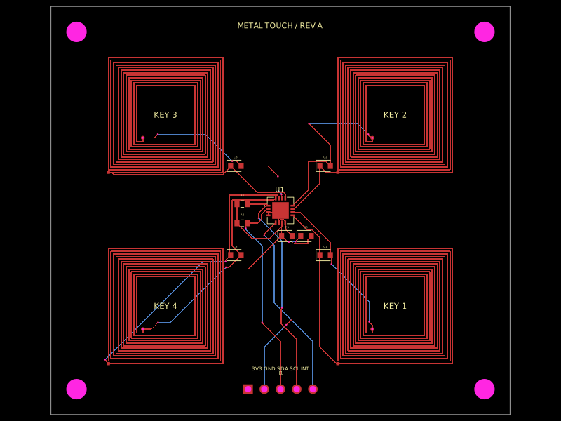 Discover something newhrithik18k/metal-touch-panelA PCB autorouting wrapper that corrects footprint-trace obstacle dimensions, solves routes with a preloaded trace-graph solver, and reports completed traces or routing errors.