rushabhcodes/ESP32-E-Reader
A compact ESP32-C3 e-reader PCB integrating LiPo charging/protection, USB-C, 3.3 V regulation, e-paper display bias generation, microSD storage, and tactile controls.
- Version
- 1.0.85
- License
- unset
- Stars
- 3
assets/enclosure/PRINTING.md
# Rev. H: two-piece, 16.8 mm snap-fit enclosure

Print **two parts**: `front-chassis` and `rear-cover`. The front chassis includes
all four navigation keys, their independent PETG spring leaves and
six releasable screen clips and four cover latch receivers. The rear cover includes
PCB cantilever bosses, four integral cover snap tabs, battery guides and two
supports for the upper display border. There is no printed tray,
separate bezel, button strip or loose display-retaining frame.

The nominal outside envelope is **68 × 116.81 × 16.8 mm**. The 3.97inch (G)
glass and active area have matching rebates, window and border supports for
up to 1.10 mm glass thickness. The ribbon stays flat for 15.00 mm, at the
manufacturer's positioning line, then wraps outside the PCB bottom edge.
The former PCB slot is removed. The lower shell end grows 1 mm from Rev. F;
thickness is unchanged. Both shells must be printed as a matched Rev. H pair.
Four integral side tabs close the cover without cover screws.
The keys sit at X ±16.5 and ±27.5 mm, beside a 23 mm rear-recessed ribbon
channel. Its 1.85 mm integral front floor protects the tail from fingers. Complete
10.2 mm key flanges clear even the full 21.28 mm ribbon root in plan view.

**PCB ordering remains blocked on screen-tail confirmation.** The new
FH34SRJ short-contact socket replaces FH12, but the full panel tolerance ranges
are not covered by its recommended FPC drawing, and the panel's pin-1 direction
and installed bend radius remain unverified. See
[display-interface-check.json](stl/display-interface-check.json) and the repository
[ordering gate](../../ORDERING.md). A clean slice proves toolpath generation,
not the real tail's mating compatibility. Treat these as fit-prototype shells.

The same protected pack is centered at X −6.0, Y −8.5 mm and attaches to the
rear cover with two nonconductive adhesive strips. The 0.2 mm insulating liner,
0.5 mm adhesive and 1.2 mm rear wall are retained.

Download [the print ZIP](esp32-reader-printable-stls.zip) or import the
[220 × 220 mm 3MF plate](reader-print-plate.3mf). It contains exactly two separate
objects, already oriented, in millimetres at 100% scale. Select your actual
printer and PETG preset. The ZIP also contains the two oriented STLs, this guide
and the geometry specifications and validation reports. No printer-specific G-code is supplied.
Files under `stl/` retain PCB coordinates for inspection. Files marked
`DO-NOT-PRINT` represent gauges, the battery, film or purchased supplies.

## Printing

Working setup: FDM with a 0.4 mm nozzle, PETG, 0.2 mm layers, three walls,
five top/bottom layers and 20% gyroid infill. PETG is required for the integral
key leaves, cover snap tabs and releasable display clips. Both shells print with their flat
outside face on the bed; no enclosure tilting or scaling is required.

Use removable snug supports, including supports that start on the part, at a
45° threshold with a 0.2 mm contact gap. The reference profile enables supports
under bridges. Inspect the six screen leaves, four button leaves, four cover
snap leaves, PCB screw features and seam tongue in the slicer. All those regions are accessible while
the shells are empty. Carefully remove support without cutting the spring
leaves. The battery pocket is open, so no support is trapped in a closed cavity.
Use your printer's calibrated temperature, cooling and speed settings. Follow
its plate instructions for PETG release layers and add a brim if required.

[fdm-reference.ini](fdm-reference.ini) records geometry-check settings; it is not
a calibrated machine preset. Prusa's guides describe [printing tolerances and
orientation](https://help.prusa3d.com/article/modeling-with-3d-printing-in-mind_164135)
and [support placement](https://help.prusa3d.com/article/support-material_1698).
The revised meshes pass the connected-solid and manifold checks. **Rev. H was
sliced with PrusaSlicer 2.9.6+arch5** using the reference profile: both STLs and
the combined 3MF produced toolpaths with no slicer warnings. The combined plate
estimate is **34.28 g PETG, including 1.471 g supports, and 4 h 7 min**;
these are reference estimates, not a prediction for a particular machine.
The [printability report](stl/printability-check.json) records source/profile
hashes and per-part results. The [toolpath inspection](stl/toolpath-check.json)
checks bed bounds, layer coverage and extrusion presence for four key springs,
six screen leaves, four cover snaps and two upper screen supports. Selected
layers were visually reviewed, including supports at the spring/overhang areas.
Generate the final toolpaths with your printer and its calibrated PETG profile.
The reference G-code is kept under ignored `checks/printability` and is not
included in the download. Fit, support removal, switch force, clip release force
and printed fatigue still require a physical prototype. The ribbon drawing
discrepancies above remain unresolved.

## Transparent cover

The actual front and rear GLBs use alpha blending: the smoke-tinted front has
0.38 opacity, and the rear has 0.22 opacity. The hosted tscircuit view and native
export apply 0.5 opacity through the explicit translucency flag on both shells.
These views show the electronics through the enclosure. That visual opacity does not
predict an actual print's optical clarity.

Clear PETG may be used for both parts. Normal FDM layers produce a translucent
cover; it will not look like glass. Keep the PETG flexures if printing the front
in another color. Resin would require separate flexibility and tolerance
validation; the included geometry and slicing checks assume PETG FDM.

## Required nonprinted supplies

- SparkFun PRT-13855 protected 1S, 3.7 V / 2000 mAh pack with mating JST-PH
  plug. The dimensioned model now shows the foil pouch and both insulated
  leads. Route the leads around the open upper end of the guides and down
  the right-side space to BT1, with red on pin 1 and black on pin 2. This
  route needs 94 mm usable free lead, including slack; verify the supplied
  cable and polarity before connecting. No additional printed part is used.
- Four M2.5 × 4 mm PCB screws, head diameter ≤5 mm and head height ≤2.5 mm.
  The board clamps against the rear-cover boss underside at Z +0.8. Screws
  enter from the display-facing side, with heads at Z −3.3…−0.8 and tips at
  Z 3.2. Prepare the nominal 2.0 mm pilots before fitting electronics.
- Display-compatible nonconductive cushioning: ten front border pads,
  installed thickness 0.15 mm; six small rear clip pads and two upper support
  pads, installed thickness 0.35 mm for the 1.10 mm CAD glass gauge. Select
  rear cushioning for the measured panel: installed thickness = 1.45 mm minus
  glass thickness (about 0.45 mm for 1.00 mm glass, 0.53 mm for 0.92 mm).
  Check gentle retention without pressure on pixels. Never place a hard clip on bare glass.
  Locations are recorded in the generator and [enclosure-design.json](enclosure-design.json).
- A 49.4 × 69 × 0.2 mm nonconductive PET or suitable equivalent liner, including
  its thin adhesive, on the PCB-facing battery surface. It is an insulating
  sheet, not a printed part. Keep edges away from connector contacts.
- Two pouch-compatible, nonconductive foam adhesive strips, nominally
  10 × 50 × 0.5 mm, to attach the battery's rear face to the inside cover.
  Use an adhesive suitable for your actual protected pack and PETG. The guides
  locate the pack; adhesive retention must be tested on the real materials.

The case uses **four internal PCB screws**, with **zero cover screws**. Hardware envelopes
are nominal; head shapes, threads, tolerances and printer shrinkage need testing.

## Assembly

1. Print, remove supports, clear/tap PCB screw pilots and inspect both empty shells.
   Dry-fit the cover and release all four tabs through the side windows with
   a plastic pick. The nominal inward release movement is 0.6 mm. Check that
   each tab springs back and its hook engages before installing electronics.
   Check all four integral keys for independent movement and return. Their
   nominal 0.25 mm key stroke includes a 0.04 mm rest gap and about 0.21 mm switch
   compression. This small modeled rest gap is below normal FDM fit tolerance:
   with the PCB installed and the screen disconnected, verify every switch is
   released at rest and actuates before its key reaches the flange stop. Tune
   the plunger/contact fit on the prototype before fitting the glass.
   A worn key requires replacing the front chassis, which is the
   tradeoff for eliminating separate printed buttons.
2. Fit the ten thin front pads to the screen ledge. Attach the six small pads to
   the undersides of the side clip lips and the two pads to the rear cover's
   upper screen supports. Spread the six side leaf tips outward using plastic
   picks, keeping force on the clips rather than the display. The CAD release
   check uses 1.0 mm lateral tip movement. Lower the panel straight into its
   rebate, then release the clips gently. They bear only on the padded border.
   Stop if the panel cannot seat or any clip presses its active area.
3. With the PCB removed, dry-fit the battery loading path. Enter through the
   open upper end of the guides with the pack centered at X −6.0, Y +1.0.
   Lift it toward the lid, leaving 0.1 mm stand-off, then slide it 9.5 mm toward
   the lower stop to Y −8.5. This passes above the lower PCB mounting bosses.
   Apply the insulating liner to the PCB-facing pack surface and use the two
   adhesive strips with accessible release pull tabs. Leave their release film
   in place while locating the pack; peel and bond once it is in position.
   Verify the real adhesive, release-film thickness and pull-tab access during
   the dry fit. Do not squeeze or bend the pouch to complete the loading path.
   The nominal 49.2 × 68.8 × 5.6 mm protected pack is centered at X −6.0,
   Y −8.5; its PCB-facing surface is Z 3.7. Guides allow 0.2 mm nominal edge
   clearance. Verify the complete pack envelope, labels, lead and adhesive fit.
4. Attach the antenna film near X 25, Y 44 on the rear cover. Seat the PCB
   straight into the rear cover from its open display-facing side, against the
   four cantilever bosses at Z +0.8. Fit the four M2.5 × 4 screws from the
   PCB underside. This leaves access to the pilots and avoids posts crossing
   the glass insertion path.
5. Bring the two loaded halves together without tension on the display tail.
   Keep the bonded/COF area flat and verify the permitted fold zones on the
   actual Waveshare tail. Keep the first 15 mm flat, then wrap outside the PCB
   bottom edge at Y −48.6. Bring the offset wing above the PCB to J2 at
   X +21.87, Y −35.08101. Socket pin 1 is on +X; supplier placement uses 0°.
   Open the latch, insert parallel to the board with exposed contacts toward
   the PCB, then close it. Proceed only after the actual panel's pin 1, tail
   tolerances, insertion depth and permitted radius have been established.
   Connect the battery to BT1: pin 1 `BATT_P` is near X 25.025, pin 2
   `BATT_N_RAW` near X 27.025 (both Y −4). Confirm actual keyed plug polarity. Route the
   battery lead through the guide notch and antenna coax to U4 without trapping
   either. Real cable slack and installation access need a physical sample.
6. Lower the loaded rear cover and attached PCB straight onto the front chassis.
   Its two upper support columns pass beyond the PCB and cushion the top
   screen border. Align the seam, then press at each latch location until all
   four hooks engage. The tongue sets alignment and the perimeter seam sets
   closure depth. Do not force a lid over a trapped wire or pack.

To open the cover, press the recessed hooks inward through the four side
windows with a plastic pick. Keep the first pair released while releasing the
other pair, then lift the loaded rear cover straight. Avoid twisting the screen
or pulling on the ribbon.

For screen service, disconnect the display tail and remove the loaded rear cover, then release the six screen clips. No loose retaining frame needs dismantling.

## Geometry and validation

The PCB origin is retained: screen/front is negative Z, battery/rear positive Z.

| Feature | Nominal dimensions / position |
| --- | --- |
| Outside | 68 × 116.81 × 16.8; X ±34, Y −51.5…65.31, Z −5.8…11.0; radius 5 |
| Front display ledge | Floor Z −4.8, 1.0 mm minimum front material; ten 0.15 mm pads |
| Panel / visible window | 56.24 × 96.62 × 1.1 / 52.8 × 87.2; glass center Y 15.31, window Y 18.22 |
| Screen pocket | 56.8 × 97.2; 0.28/0.29 mm nominal edge clearance |
| Side clips | Six; tip Y −22, 3, 27; 14 mm spring leaves; padded face Z −3.2 |
| Upper rear supports | X ±12, Y 62.65; padded face Z −3.2, beyond the PCB outline |
| PCB | 62.5 × 95.08 × 1.6; Z ±0.8; four mounts: upper (±27, 44.75), lower (−25.5, −36.5)/(+28, −29) |
| Shell seam | Z 5.4; 0.2 mm side tongue clearance and 0.3 mm end clearance |
| Rear outside face | Z 11.0; 1.2 mm flat cover, with four integral snap leaves |
| Battery stack | 0.2 mm liner at Z 3.5…3.7; cell at 3.7…9.3; 0.5 mm adhesive to Z 9.8 |
| Guides | 0.8 mm; side X −31.2/19.2; lower stop Y −43.5; upper loading end open |
| Cover snaps | Four; sides X ±32.6, tip Y −5/24; 14 mm beams, 0.8 mm thick |
| Snap engagement / release | 0.4 mm radial engagement; 0.2 mm vertical play; 0.6 mm inward release |
| Snap receivers | 0.8 mm retaining walls; accessible 6 × 1.5 mm side windows |
| USB/SD/switch access | Front-wall openings reach the seam to clear the attached PCB at closure |

The lower PCB mounting bosses set this revision's height limit. The liner
has 0.25 mm nominal clearance above their Z 3.25 tops and above
L1 and other electronic bodies under the shifted battery (see the clearance report). Its edge is 1.63 mm
below the ESP32 module in Y. During loading, the 0.1 mm lid stand-off leaves
0.15 mm nominal clearance over the lower bosses.
The same battery capacity and insulation are retained. Confirm the actual pack
thickness and clearance on a prototype, including any swelling allowance;
do not force closure onto the pack. Actual battery cables, antenna coax,
printed shrinkage, adhesive strength and flexure fatigue are not simulated.
The snap checks verify hook retention, geometric release, and sampled closing
and opening paths. They do not predict snap force or cycle life.

Regenerate and verify using:

```sh
blender --background --python-exit-code 1 --python scripts/generate-printable-enclosure.py
bun run build
bun run export:assembly
blender --background --python-exit-code 1 --python scripts/check-enclosure-clearance.py -- dist/index/assembly.glb
blender --background --python-exit-code 1 --python scripts/check-display-connection.py -- dist/index/assembly.glb
python3 scripts/check-printability.py /path/to/prusa-slicer
python3 scripts/inspect-print-toolpaths.py
python3 scripts/check-display-interface.py
blender --background --python-exit-code 1 --python scripts/render-printable-enclosure.py
```

Generated reports under `stl/` record mesh integrity, nominal clearances,
independent key strokes, sampled screen/PCB/battery/cover assembly paths,
CAD transparency and slicer output. The source still contains the original
supplier STEP models; the hosted STEP archives ([1](../components/supplier-step-models-1.zip), [2](../components/supplier-step-models-2.zip), [3](../components/supplier-step-models-3.zip), [4](../components/supplier-step-models-4.zip))
preserve them without loading large STEP duplicates in the browser preview.
Related Packages
 More from this authorrushabhcodes/tetrisThis code defines various electronic component models—including a AAA battery holder, ATtiny85 microcontroller, switch, buzzer, display, and resistors—as hardware modules with detailed footprints, pin configurations, CAD models, and physical specifications for use in circuit design.
 Similar packagemohan-bee/esp32-c3This hardware design integrates an ESP32-C3 microcontroller, a USB-C connector, a power management IC (AP2112-3.3V regulator), a USB-to-Serial converter (CH340C), several resistors, capacitors, and user-accessible headers to facilitate USB communication, power regulation, and general I/O interfacing.
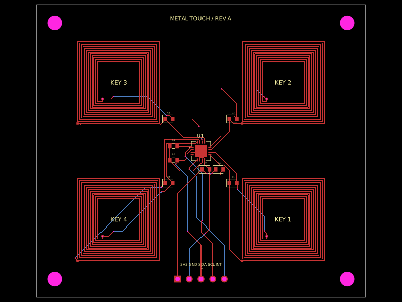 Discover something newhrithik18k/metal-touch-panelA PCB autorouting wrapper that corrects footprint-trace obstacle dimensions, solves routes with a preloaded trace-graph solver, and reports completed traces or routing errors.