runpatrick/sa-sim-pcb
This code defines PCB footprints for various electronic modules, including BG95 cellular modem, BNO086 sensor, BQ25180 battery charger, and BQ27220 power management IC, detailing their physical pad layouts and key external features.
- Version
- 1.0.6
- License
- unset
- Stars
- 0
sim/jlcpcb-dfm.md
# SA-SIM v1 — JLCPCB DFM Compliance

**Process:** JLCPCB 4-layer, 1.6 mm FR-4, 1oz outer / 0.5oz inner
**Board:** SA-SIM v1, 40 mm × 40 mm
**Audit date:** 2026-04-30

---

## Rule Compliance Table

| Rule | JLCPCB Min | SA-SIM v1 | Status |
|---|---|---|---|
| Trace width | 0.127 mm (5 mil) | 0.15 mm (signal) / 0.30 mm (power) min | PASS |
| Trace spacing | 0.127 mm | 0.15 mm default | PASS |
| Drill diameter | 0.20 mm (8 mil) | 0.30 mm via default | PASS |
| Via annular ring | 0.05 mm | 0.075 mm | PASS |
| Min hole-to-edge | 0.30 mm | 1.5 mm IP68 outer keepout >> 0.3 mm | PASS |
| Min board size | 5×5 mm | 50×50 mm | PASS |
| Max board size | 400×500 mm | 50×50 mm | PASS |
| Silk min line | 0.15 mm | accept default | PASS |
| Silk min char | 0.8 mm | accept default | PASS |
| Solder mask dam | 0.10 mm | accept default | PASS |
| Stack-up | 4-layer 1.6 mm FR-4 | requested | PASS |
| Copper weight | 1oz outer / 0.5oz inner | requested | PASS |

---

## Notes on Marginal Items

### Trace Width — Signal Nets

The design enforces 0.15 mm minimum on all signal traces (I2C, UART, SWD), which gives 18% clearance above the JLCPCB 5 mil (0.127 mm) floor. The USB_DM/DP differential pair uses 0.18 mm traces with a 0.10 mm edge-to-edge gap; gap is just above the 0.127 mm floor and does not require a controlled-impedance surcharge.

### Drill / Via

All vias are 0.30 mm drill (12 mil), which clears the 0.20 mm (8 mil) minimum. Annular ring of 0.075 mm (0.30 mm pad diameter − 0.30 mm drill / 2 = 0.075 mm half-ring) clears the 0.05 mm minimum. JLCPCB standard process allows 0.30 mm drill without additional cost.

### BG95 LGA-96 Pad Density

The BG95-M3 LGA-96 footprint has a 0.8 mm pad pitch on a 23.6×19.9 mm body. The smallest inter-pad gap in the LGA array is approximately 0.35 mm (0.8 mm pitch − 0.45 mm pad width), which is above the 0.127 mm solder mask dam minimum. JLCPCB can manufacture this footprint; however, the LGA paste deposition and solder joint inspection require care — use JLCPCB's X-ray inspection option (available as add-on) for this component specifically.

### IP68 Keepout Ring

The 1.5 mm outer keepout ring prevents any traces, vias, or copper pour within 1.5 mm of the board edge. This greatly exceeds the 0.30 mm hole-to-edge minimum and is the controlling constraint (IP68 potting, not DFM).

### BQ25180 WCSP-9 and BQ27220 DSBGA-12

Both are ultra-small packages (1.62×1.58 mm, 0.5 mm pitch and 1.92×1.62 mm, 0.4 mm pitch respectively). JLCPCB assembly supports 0.4 mm pitch with standard SMT; confirm BQ27220 DSBGA is within JLCPCB's minimum pad pitch capability (stated minimum 0.35 mm for micro-BGA). If JLCPCB rejects BQ27220 DSBGA footprint at the DFM stage, an alternative DSBGA-to-QFN breakout substrate or a different package variant (BQ27220YZFR exists only in DSBGA — check if TI offers a YZF variant with larger pads) may be required.

---

## Pre-Fab Checklist

Before submitting Gerbers to JLCPCB:

1. **Run JLCPCB Gerber Viewer DFM** after export — upload the full Gerber + drill ZIP to [jlcpcb.com](https://jlcpcb.com) and review the automated DFM report. Pay attention to any flagged clearance violations or missing solder mask openings.

2. **Verify drill report for minimum drill size** — open the Excellon drill file and confirm no drill entry is below 0.28 mm (28 mil). JLCPCB's automated DFM flags drill < 8 mil (0.20 mm), but any production drill < 0.30 mm should be reviewed for cost impact (smaller drills require slower feed rates and have a higher breakage rate).

3. **Silk-on-pad check** — confirm no silkscreen lines or reference designator text overlap copper pads. JLCPCB's DFM will flag silk-on-pad; the most likely offenders are the BG95 LGA reference designator (U2 text inside the 23.6×19.9 mm outline) and the BQ51013 QFN-28 (IC2).

4. **Pad-to-pad clearance check at BG95 LGA** — in the Gerber viewer, zoom into the BG95 LGA-96 footprint and verify that copper pads from adjacent components (particularly C_BG95_BAT1/2/3 decoupling capacitors) maintain at least 0.15 mm clearance from the LGA pad array outer row.

5. **Paste layer check** — verify the F.Paste layer has openings for all SMT pads and no extraneous paste on vias or test points. The BQ25180 WCSP-9 and BQ27220 DSBGA-12 paste openings must be present.

6. **Order specification confirmation** — on the JLCPCB order form, explicitly select: 4-layer, 1.6 mm, FR-4, 1oz outer / 0.5oz inner copper, ENIG surface finish (gold, preferred over HASL for fine-pitch LGA), green solder mask, white silkscreen. Request X-ray inspection as add-on for BG95 LGA solder joint verification.
Related Packages
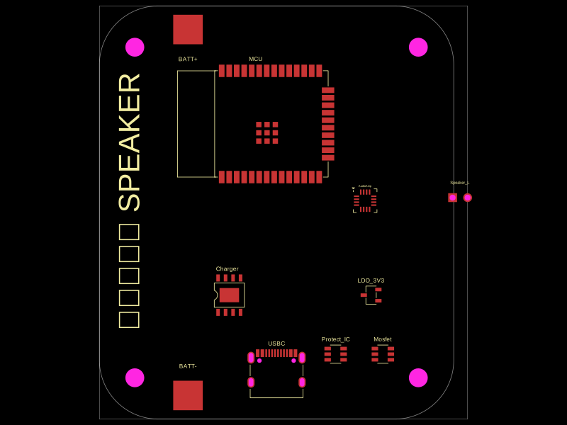 Similar packagemohan-bee/speakerThis code defines configurable 3D models and PCB footprints for various electronic components, including a battery charger IC, a dual Hall sensor, a dual power switch, and a voltage regulator, with detailed pinouts, footprints, and CAD models for schematic and physical design.
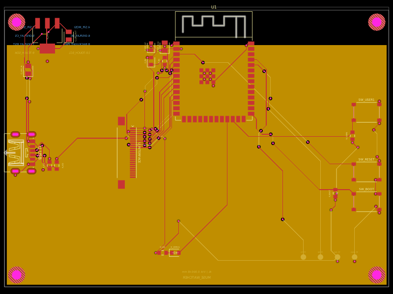 Discover something newShiboSoftwareDev/muse-sensecap-watcher-replacementA 4-layer ESP32-S3 carrier board with USB-C power, AMS1117 3.3V regulation, reset/boot/user buttons, status LED, capacitors/resistors, and a 24-pin FFC interface.