runpatrick/sa-sim-pcb
This code defines PCB footprints for various electronic modules, including BG95 cellular modem, BNO086 sensor, BQ25180 battery charger, and BQ27220 power management IC, detailing their physical pad layouts and key external features.
- Version
- 1.0.6
- License
- unset
- Stars
- 0
footprints/tps62840.tsx
// TPS62840 X2SON-8 (DSG) 1.5×2.0mm body, 0.5mm pitch
// 4 pads each side (left/right only), 0.26×0.35mm pads
// Pin map (TI SLVSEC6D):
//   1=VIN   2=EN    3=MODE  4=AGND
//   5=PGND  6=SW    7=FB    8=VOS

export const tps62840Footprint = () => (
  <footprint>
    {/* LEFT side: pins 1-4, x=-0.85, y from +0.75 step -0.5 */}
    {[0, 1, 2, 3].map((i) => (
      <smtpad
        portHints={[String(i + 1)]}
        shape="rect"
        width="0.35mm"
        height="0.26mm"
        pcbX="-0.85mm"
        pcbY={`${0.75 - i * 0.5}mm`}
        layer="top"
      />
    ))}
    {/* RIGHT side: pins 5-8 (CCW), x=+0.85, y from -0.75 step +0.5 */}
    {[0, 1, 2, 3].map((i) => (
      <smtpad
        portHints={[String(i + 5)]}
        shape="rect"
        width="0.35mm"
        height="0.26mm"
        pcbX="0.85mm"
        pcbY={`${-0.75 + i * 0.5}mm`}
        layer="top"
      />
    ))}

    <silkscreenpath
      route={[
        { x: -0.75, y: -1.0 },
        { x: 0.75, y: -1.0 },
        { x: 0.75, y: 1.0 },
        { x: -0.75, y: 1.0 },
        { x: -0.75, y: -1.0 },
      ]}
    />
  </footprint>
)
Related Packages
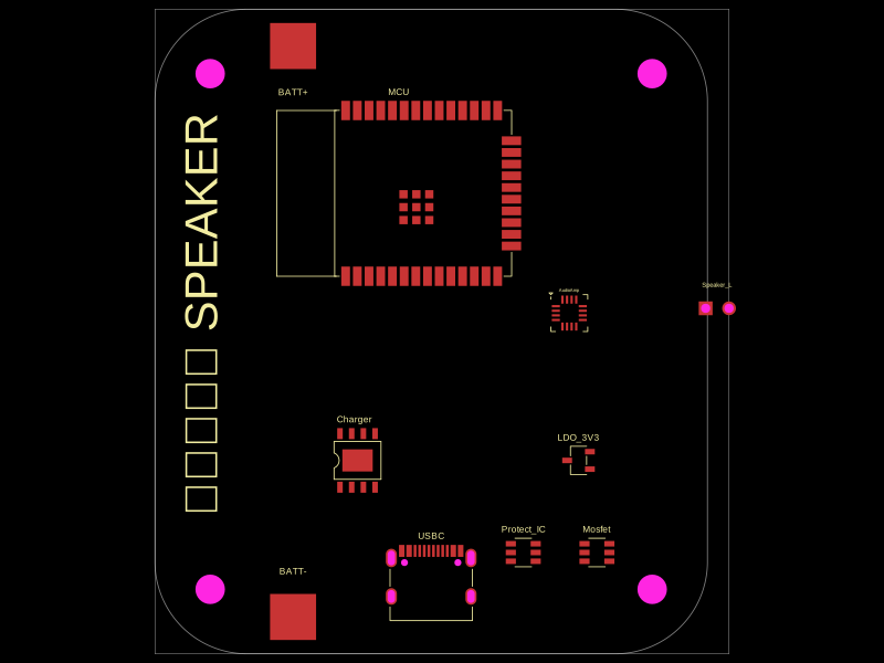 Similar packagemohan-bee/speakerThis code defines configurable 3D models and PCB footprints for various electronic components, including a battery charger IC, a dual Hall sensor, a dual power switch, and a voltage regulator, with detailed pinouts, footprints, and CAD models for schematic and physical design.
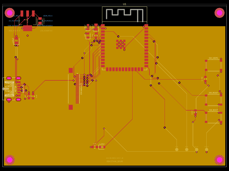 Discover something newShiboSoftwareDev/muse-sensecap-watcher-replacementA 4-layer ESP32-S3 carrier board with USB-C power, AMS1117 3.3V regulation, reset/boot/user buttons, status LED, capacitors/resistors, and a 24-pin FFC interface.