pixalynx/usbc-led-switch
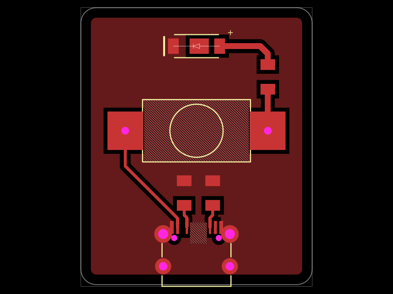
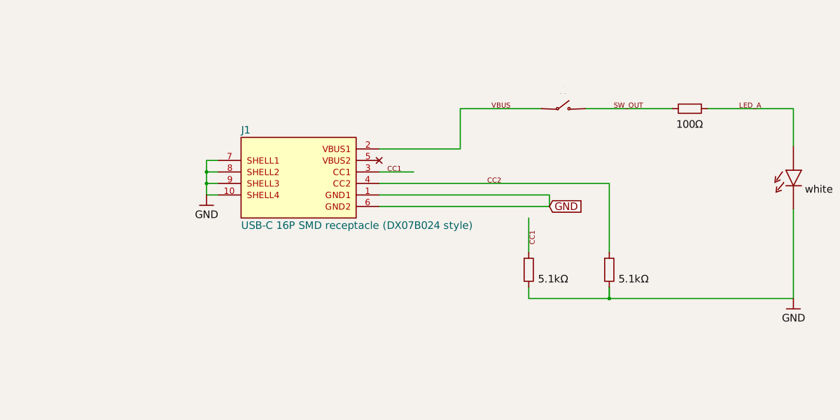
A single-sided USB-C–powered LED light board with a latching pushbutton, 100 Ω current-limiting resistor, white 5730 SMD LED, and dual 5.1 kΩ USB-C CC pull-down resistors.
- Version
- 0.0.1
- License
- unset
- Stars
- 0
index.circuit.tsx
PCB
Schematic
import { CAD } from "./lib/cad-models"
import { LED5730, LG15F, R1206V, SW_PINS, USBC_PINS, UsbC16pMill } from "./lib/footprints"

/**
 * USB-C LED light, single-sided, for isolation milling.
 *
 *   USB-C VBUS --> SW1 (push-on/push-off) --> R3 100R --> LED1 (white 5730) --> GND
 *   USB-C CC1 --> R1 5.1k --> GND,  CC2 --> R2 5.1k --> GND   (makes USB-C chargers switch 5 V on)
 *
 * Everything sits on the copper (top) side. GND is a copper pour, so only VBUS, CC1, CC2 and the LED chain
 * are traces. All parts are at rotation 0 so every pcbPath below is board coordinates minus the centre of the
 * trace's `from` part.
 */

const W = 30
const H = 36
const EDGE = 0.8 // pour inset from the board edge

// Part centres (board mm, origin at board centre, +y away from the USB-C mouth)
const J1 = { x: 0, y: -13 } // mouth at y = -18.225 (0.225 mm proud of the edge); lands at y = -10.575
const R1 = { x: -1.6, y: -6.1 } // upright 1206, pin1 (CC end) at the bottom
const R2 = { x: 2.1, y: -6.1 }
const SW1 = { x: 0, y: 2 } // tabs at x = -9.25 (VBUS in) and +9.25 (out)
const R3 = { x: 9.25, y: 9 } // upright 1206 straight above SW1's right tab
const LED1 = { x: 0, y: 13 } // anode at +x

type P = { x: number; y: number }
/** Board-coordinate waypoints -> pcbPath in the `from` part's frame (all parts are unrotated). */
const rel = (c: P, pts: P[]) => pts.map((p) => ({ x: +(p.x - c.x).toFixed(4), y: +(p.y - c.y).toFixed(4) }))

const roundRect = (w: number, h: number, r: number, n = 6): P[] => {
  const pts: P[] = []
  const corners = [
    [w / 2 - r, h / 2 - r, 0],
    [-w / 2 + r, h / 2 - r, 90],
    [-w / 2 + r, -h / 2 + r, 180],
    [w / 2 - r, -h / 2 + r, 270],
  ] as const
  for (const [cx, cy, a0] of corners)
    for (let i = 0; i <= n; i++) {
      const a = ((a0 + (90 * i) / n) * Math.PI) / 180
      pts.push({ x: +(cx + r * Math.cos(a)).toFixed(4), y: +(cy + r * Math.sin(a)).toFixed(4) })
    }
  return pts
}

export default () => (
  <board
    width={`${W}mm`}
    height={`${H}mm`}
    layers={1}
    thickness="1.5mm"
    borderRadius="2mm"
    routingDisabled
    minTraceWidth="0.4mm"
    minTraceToPadEdgeClearance="0.3mm"
    minPadEdgeToPadEdgeClearance="0.3mm"
    minBoardEdgeClearance="0.5mm"
  >
    <connector
      name="J1"
      pinLabels={USBC_PINS}
      footprint={<UsbC16pMill />}
      cadModel={CAD.usbc16p}
      pcbX={J1.x}
      pcbY={J1.y}
      schX={-4}
      schY={0}
      schWidth={2}
      schPinArrangement={{
        rightSide: { direction: "top-to-bottom", pins: ["VBUS1", "VBUS2", "CC1", "CC2", "GND1", "GND2"] },
        leftSide: { direction: "top-to-bottom", pins: ["SHELL1", "SHELL2", "SHELL3", "SHELL4"] },
      }}
      manufacturerPartNumber="USB-C 16P SMD receptacle (DX07B024 style)"
      connections={{ GND1: "net.GND", GND2: "net.GND", SHELL1: "net.GND", SHELL2: "net.GND", SHELL3: "net.GND", SHELL4: "net.GND" }}
      noConnect={["VBUS2"]}
    />
    <resistor name="R1" resistance="5.1k" footprint={<R1206V />} cadModel={CAD.r1206v} pcbX={R1.x} pcbY={R1.y} schX={0} schY={-1.6} schRotation={-90} connections={{ pin2: "net.GND" }} />
    <resistor name="R2" resistance="5.1k" footprint={<R1206V />} cadModel={CAD.r1206v} pcbX={R2.x} pcbY={R2.y} schX={1.4} schY={-1.6} schRotation={-90} connections={{ pin2: "net.GND" }} />
    <switch name="SW1" type="spst" pinLabels={SW_PINS} footprint={<LG15F />} cadModel={CAD.lg15f} pcbX={SW1.x} pcbY={SW1.y} schX={0.6} schY={1.2}
      manufacturerPartNumber="LG-15F (Adafruit 3870)" />
    <resistor name="R3" resistance="100" footprint={<R1206V />} cadModel={CAD.r1206v} pcbX={R3.x} pcbY={R3.y} schX={2.8} schY={1.2} />
    {/* tscircuit LED: pin1 = anode, pin2 = cathode */}
    <led name="LED1" color="white" footprint={<LED5730 />} cadModel={CAD.led5730} pcbX={LED1.x} pcbY={LED1.y} schX={4.6} schY={0} schRotation={-90} connections={{ pin2: "net.GND" }} />

    {/* 0.4 mm where a trace leaves a USB-C land (the lands are 0.3-0.4 mm wide with 0.30 mm gaps) */}
    <trace name="CC1" from=".J1 > .CC1" to=".R1 > .pin1" thickness="0.4mm" pcbPath={rel(J1, [{ x: -1.25, y: -9.3 }, { x: -1.6, y: -8.95 }])} />
    <trace name="CC2" from=".J1 > .CC2" to=".R2 > .pin1" thickness="0.4mm" pcbPath={rel(J1, [{ x: 1.75, y: -9.3 }, { x: 2.1, y: -8.95 }])} />
    <trace name="VBUS" from=".J1 > .VBUS1" to=".SW1 > .pin1" thickness="0.4mm" pcbPath={rel(J1, [{ x: -2.45, y: -9.4 }, { x: -9.25, y: -2.6 }])} />
    {/* Switched side: 0.8 mm */}
    <trace name="SW_OUT" from=".SW1 > .pin2" to=".R3 > .pin1" thickness="0.8mm" pcbPath={rel(SW1, [{ x: 9.25, y: 5.6 }])} />
    <trace name="LED_A" from=".R3 > .pin2" to=".LED1 > .pin1" thickness="0.8mm" pcbPath={rel(R3, [{ x: 9.25, y: 12 }, { x: 8.25, y: 13 }])} />

    <copperpour layer="top" connectsTo="net.GND" clearance="0.5mm" outline={roundRect(W - 2 * EDGE, H - 2 * EDGE, 2 - EDGE)} />
    {/* No copper under the six unused D+/D-/SBU contacts of J1 (they have no lands) ... */}
    <keepout shape="rect" layer="top" pcbX={0.25} pcbY={-11.3} width={2.2} height={2.8} />
    {/* ... nor under the switch body, whose underside is not documented */}
    <keepout shape="rect" layer="top" pcbX={SW1.x} pcbY={SW1.y} width={13.6} height={8.1} />
  </board>
)
Related Packages
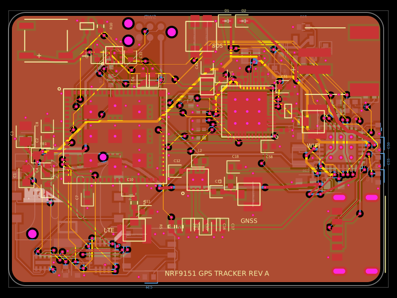 More from this authorpixalynx/nrf9151-gps-trackerA compact 44×32 mm, 4-layer nRF9151 LTE-M/NB-IoT/GNSS tracker PCB with nPM1300 LiPo/USB-C power, nano-SIM/eSIM switching, nRF7002 Wi‑Fi scanning, accelerometer, antennas, buzzer, LEDs, SOS button, and SWD/debug connectors.
 Similar packagegokul/usb-hub-boardA 4-layer 100×66 mm USB 2.0 hub board with a USB‑C upstream port, four protected downstream USB‑C/USB‑A ports, an integrated SD card reader, USB hub controllers, 3.3 V regulation, ESD protection, current-limited power switches, crystal oscillators, and filtering/passive components.
 Discover something newhrithik18k/smart-switch-pcbThe AO3400A component models a SOT-23 N-channel MOSFET with labeled pins for Gate, Source, and Drain, including 3D CAD models and schematic symbols for electronic circuit design.