pixalynx/usbc-led-switch
A single-sided USB-C–powered LED light board with a latching pushbutton, 100 Ω current-limiting resistor, white 5730 SMD LED, and dual 5.1 kΩ USB-C CC pull-down resistors.
- Version
- 0.0.1
- License
- unset
- Stars
- 0
dist/index.js
import { jsx, jsxs } from 'react/jsx-runtime';
import m_usbc16p from '././assets/usbc16p-f52e6704.obj';
import m_r1206v from '././assets/r1206v-c97b80df.obj';
import m_led5730 from '././assets/led5730-4b07577b.obj';
import m_lg15f from '././assets/lg15f-967a4f49.obj';
import { Fragment } from 'react';

// Generated by scripts/gen-cad-models.py. Do not edit.
// modelOriginPosition = the model-frame point placed on the board surface at the land-pattern centre.
const CAD = {
    usbc16p: { objUrl: m_usbc16p, pcbRotationOffset: 0, modelOriginPosition: { x: -0, y: 1.3749, z: -1.68 } }, // C2765186 USB-C-SMD_TYPE-C-6PIN-2MD-073 (EasyEDA)
    r1206v: { objUrl: m_r1206v, pcbRotationOffset: 0, modelOriginPosition: { x: 0.0, y: 0.0, z: 0.0 } }, // 1206 chip resistor, 3.2 x 1.6 x 0.55
    led5730: { objUrl: m_led5730, pcbRotationOffset: 0, modelOriginPosition: { x: 0.0, y: 0.0, z: 0.0 } }, // 5730 LED, Yuji YJ-BC-5730L-G02 outline
    lg15f: { objUrl: m_lg15f, pcbRotationOffset: 0, modelOriginPosition: { x: 0.0, y: 0.0, z: 0.0 } }, // Legong LG-15F / Adafruit 3870, from the Legong drawing
};

/** Land patterns for a home-milled, single-sided board. Millimetres, top view, +y up.
 *
 * Isolation milling has no solder mask and no plating, so every land here is drawn bigger than a fab
 * footprint would be, gaps are kept at 0.30 mm or more, and through-holes are round (drill bits, not slots)
 * with their copper ring on the top (component) side only.
 */
const keyed = (els) => els.map((e, i) => jsx(Fragment, { children: e }, e.key ?? `n${i}`));
const fp = (els) => jsx("footprint", { children: keyed(els) });
const pad = (pin, x, y, w, h) => (jsx("smtpad", { portHints: typeof pin === "string" ? [pin] : pin, pcbX: x, pcbY: y, width: w, height: h, shape: "rect" }));
/** Round hole with a top-side ring. tscircuit calls it a plated hole; on the milled board it is a drilled hole
 * whose lead is soldered to the ring from the top. */
const thPad = (pin, x, y, drill, ring) => (jsx("platedhole", { portHints: [pin], pcbX: x, pcbY: y, holeDiameter: drill, outerDiameter: ring, shape: "circle" }));
const npth = (x, y, d) => jsx("hole", { pcbX: x, pcbY: y, diameter: d });
const silk = (pts, stroke = 0.15) => (jsx("silkscreenpath", { route: pts.map(([x, y]) => ({ x, y })), strokeWidth: stroke }));
const box = (w, h, cx = 0, cy = 0, stroke = 0.15) => silk([[cx - w / 2, cy - h / 2], [cx + w / 2, cy - h / 2], [cx + w / 2, cy + h / 2], [cx - w / 2, cy + h / 2], [cx - w / 2, cy - h / 2]], stroke);
const courtyard = (w, h, cx = 0, cy = 0) => (jsx("courtyardoutline", { outline: [
        { x: cx - w / 2, y: cy + h / 2 }, { x: cx + w / 2, y: cy + h / 2 }, { x: cx + w / 2, y: cy - h / 2 },
        { x: cx - w / 2, y: cy - h / 2 }, { x: cx - w / 2, y: cy + h / 2 },
    ] }));
const text = (t, x, y, size = 0.8) => (jsx("silkscreentext", { text: t, pcbX: x, pcbY: y, fontSize: size, anchorAlignment: "center" }));
/** The same land turned upright (pin1 at -y), so the part can stay at rotation 0. */
const R1206V = () => fp([pad("pin1", 0, -1.6, 1.9, 1.4), pad("pin2", 0, 1.6, 1.9, 1.4), courtyard(2.3, 5.0)]);
// -------------------------------------------------------------------------------------------------
// USB-C 16-pin top-mount receptacle (the generic "TYPE-C 16P" phone-repair part, same land pattern as
// JLCPCB C2765186 / HRO TYPE-C-31-M-12). Origin = connector centre line, contact row at y = +2.125,
// mouth (front of the shell) at y = -5.225.
//
// Power-only, milling-friendly variant:
// * Only GND, VBUS, CC1, CC2, VBUS, GND get lands. The six D+/D-/SBU contacts have NO land: they are not
//   needed to draw power, and leaving them out turns the 0.20 mm gaps of the stock pattern into >= 0.30 mm.
//   Their legs simply rest on bare board.
// * Lands are stretched 0.6 mm rearwards (soldering-iron room). GND lands are 0.5 wide; VBUS lands are 0.4 wide
//   and sit 0.05 mm outboard of the contact centre, so VBUS-GND is 0.30 mm and CC2-VBUS2 is 0.35 mm.
// * Shell legs: round drilled holes instead of plated slots (rear legs 1.3 mm, front legs 1.1 mm) with a
//   top-side ring to solder the leg to. The rear rings merge into the GND lands, so the shell is grounded.
// * Locating pegs: 0.8 mm holes (the pegs are 0.65-0.7 mm).
// -------------------------------------------------------------------------------------------------
const USBC_PINS = {
    pin1: ["GND1"], pin2: ["VBUS1"], pin3: ["CC1"], pin4: ["CC2"], pin5: ["VBUS2"], pin6: ["GND2"],
    pin7: ["SHELL1"], pin8: ["SHELL2"], pin9: ["SHELL3"], pin10: ["SHELL4"],
};
const LAND_Y = 2.425; // 1.575 .. 3.275: stock land front edge kept, back edge moved 0.6 mm rearwards
const LAND_L = 1.7;
const UsbC16pMill = () => fp([
    pad("pin1", -3.2, LAND_Y, 0.5, LAND_L),
    pad("pin2", -2.45, LAND_Y, 0.4, LAND_L),
    pad("pin3", -1.25, LAND_Y, 0.3, LAND_L),
    pad("pin4", 1.75, LAND_Y, 0.3, LAND_L),
    pad("pin5", 2.45, LAND_Y, 0.4, LAND_L),
    pad("pin6", 3.2, LAND_Y, 0.5, LAND_L),
    thPad("pin7", -4.325, 1.575, 1.3, 2.3),
    thPad("pin8", 4.325, 1.575, 1.3, 2.3),
    thPad("pin9", -4.325, -2.625, 1.1, 2.1),
    thPad("pin10", 4.325, -2.625, 1.1, 2.1),
    npth(-2.89, 1.055, 0.8),
    npth(2.89, 1.055, 0.8),
    // Shell outline (8.94 wide, mouth at -5.225) and a marker for the unused, land-free contacts
    silk([[-4.47, -5.225], [4.47, -5.225]]),
    silk([[-4.47, -1.4], [-4.47, 0.35]]),
    silk([[4.47, -1.4], [4.47, 0.35]]),
    silk([[-4.47, -5.225], [-4.47, -3.85]]),
    silk([[4.47, -5.225], [4.47, -3.85]]),
    courtyard(11.1, 8.9, 0, -1.05),
]);
// -------------------------------------------------------------------------------------------------
// White 5730 SMD LED (5.7 x 3.0 mm, the Amazon "Coliao" 5730 white). Land pattern from the Yuji
// YJ-BC-5730L-G02 and Sunrom 5730 datasheets: two 1.1 x 1.7 electrodes 6.8 mm overall plus a 2.5 x 1.7 heat
// pad offset towards the anode (centres anode 2.85, heat pad 0.35, cathode -2.85). Drawn rotated 180 deg from
// the datasheet so the anode is at +x, electrodes stretched 0.3 mm outwards and all pads 2.0 mm tall for
// hand soldering. The heat pad is an isolated land with no net: both datasheets show it tied to the anode
// inside the LED, but unbranded parts vary and at 20 mA it carries no heat worth sinking, so it is
// soldered for grip only. The chamfered corner on top of the LED marks the CATHODE (-x here).
// -------------------------------------------------------------------------------------------------
const LED5730 = () => fp([
    pad(["pin1", "anode"], 3.0, 0, 1.4, 2.0),
    jsx("smtpad", { pcbX: 0.35, pcbY: 0, width: 2.5, height: 2.0, shape: "rect" }),
    pad(["pin2", "cathode"], -3, 0, 1.4, 2.0),
    silk([[-2.85, 1.5], [2.85, 1.5]]),
    silk([[-2.85, -1.5], [2.85, -1.5]]),
    silk([[-4.2, 1.2], [-4.2, -1.2]], 0.25), // cathode bar
    text("+", 4.4, 1.8, 1.0),
    courtyard(8.0, 3.6),
]);
// -------------------------------------------------------------------------------------------------
// Push-on / push-off switch: Adafruit 3870 = Yueqing Legong LG-15F (Core Electronics "Mini On/Off Push-Button
// Switch"). SPST latching, 5-8 N actuation, 1.0 mm travel. Drawing: base 14.0 x 8.1 mm, two flat tabs 4.3 mm
// wide, 23.0 mm overall, tab-hole centres 18.5 mm apart, tabs 0.2 mm below the body base, so the part lies flat
// on the copper side like an SMD part. Each tab gets a 4.6 x 5.0 land; the 1.0 mm hole at the tab-hole centre
// is optional - thread a resistor-lead offcut through tab and board, bend it under, solder it on top for extra
// grip on milled copper.
// -------------------------------------------------------------------------------------------------
const SW_PINS = { pin1: ["A"], pin2: ["B"] };
const tab = (pin, x) => (jsx("platedhole", { portHints: [pin], pcbX: x, pcbY: 0, shape: "circular_hole_with_rect_pad", holeDiameter: 1.0, rectPadWidth: 4.6, rectPadHeight: 5.0 }));
const LG15F = () => fp([
    tab("pin1", -9.25),
    tab("pin2", 9.25),
    box(14.0, 8.1),
    jsx("silkscreencircle", { pcbX: 0, pcbY: 0, radius: 3.45, strokeWidth: 0.15 }),
    courtyard(23.6, 8.6),
]);

/**
 * USB-C LED light, single-sided, for isolation milling.
 *
 *   USB-C VBUS --> SW1 (push-on/push-off) --> R3 100R --> LED1 (white 5730) --> GND
 *   USB-C CC1 --> R1 5.1k --> GND,  CC2 --> R2 5.1k --> GND   (makes USB-C chargers switch 5 V on)
 *
 * Everything sits on the copper (top) side. GND is a copper pour, so only VBUS, CC1, CC2 and the LED chain
 * are traces. All parts are at rotation 0 so every pcbPath below is board coordinates minus the centre of the
 * trace's `from` part.
 */
const W = 30;
const H = 36;
const EDGE = 0.8; // pour inset from the board edge
// Part centres (board mm, origin at board centre, +y away from the USB-C mouth)
const J1 = { x: 0, y: -13 }; // mouth at y = -18.225 (0.225 mm proud of the edge); lands at y = -10.575
const R1 = { x: -1.6, y: -6.1 }; // upright 1206, pin1 (CC end) at the bottom
const R2 = { x: 2.1, y: -6.1 };
const SW1 = { x: 0, y: 2 }; // tabs at x = -9.25 (VBUS in) and +9.25 (out)
const R3 = { x: 9.25, y: 9 }; // upright 1206 straight above SW1's right tab
const LED1 = { x: 0, y: 13 }; // anode at +x
/** Board-coordinate waypoints -> pcbPath in the `from` part's frame (all parts are unrotated). */
const rel = (c, pts) => pts.map((p) => ({ x: +(p.x - c.x).toFixed(4), y: +(p.y - c.y).toFixed(4) }));
const roundRect = (w, h, r, n = 6) => {
    const pts = [];
    const corners = [
        [w / 2 - r, h / 2 - r, 0],
        [-w / 2 + r, h / 2 - r, 90],
        [-w / 2 + r, -h / 2 + r, 180],
        [w / 2 - r, -h / 2 + r, 270],
    ];
    for (const [cx, cy, a0] of corners)
        for (let i = 0; i <= n; i++) {
            const a = ((a0 + (90 * i) / n) * Math.PI) / 180;
            pts.push({ x: +(cx + r * Math.cos(a)).toFixed(4), y: +(cy + r * Math.sin(a)).toFixed(4) });
        }
    return pts;
};
var index_circuit = () => (jsxs("board", { width: `${W}mm`, height: `${H}mm`, layers: 1, thickness: "1.5mm", borderRadius: "2mm", routingDisabled: true, minTraceWidth: "0.4mm", minTraceToPadEdgeClearance: "0.3mm", minPadEdgeToPadEdgeClearance: "0.3mm", minBoardEdgeClearance: "0.5mm", children: [jsx("connector", { name: "J1", pinLabels: USBC_PINS, footprint: jsx(UsbC16pMill, {}), cadModel: CAD.usbc16p, pcbX: J1.x, pcbY: J1.y, schX: -4, schY: 0, schWidth: 2, schPinArrangement: {
                rightSide: { direction: "top-to-bottom", pins: ["VBUS1", "VBUS2", "CC1", "CC2", "GND1", "GND2"] },
                leftSide: { direction: "top-to-bottom", pins: ["SHELL1", "SHELL2", "SHELL3", "SHELL4"] },
            }, manufacturerPartNumber: "USB-C 16P SMD receptacle (DX07B024 style)", connections: { GND1: "net.GND", GND2: "net.GND", SHELL1: "net.GND", SHELL2: "net.GND", SHELL3: "net.GND", SHELL4: "net.GND" }, noConnect: ["VBUS2"] }), jsx("resistor", { name: "R1", resistance: "5.1k", footprint: jsx(R1206V, {}), cadModel: CAD.r1206v, pcbX: R1.x, pcbY: R1.y, schX: 0, schY: -1.6, schRotation: -90, connections: { pin2: "net.GND" } }), jsx("resistor", { name: "R2", resistance: "5.1k", footprint: jsx(R1206V, {}), cadModel: CAD.r1206v, pcbX: R2.x, pcbY: R2.y, schX: 1.4, schY: -1.6, schRotation: -90, connections: { pin2: "net.GND" } }), jsx("switch", { name: "SW1", type: "spst", pinLabels: SW_PINS, footprint: jsx(LG15F, {}), cadModel: CAD.lg15f, pcbX: SW1.x, pcbY: SW1.y, schX: 0.6, schY: 1.2, manufacturerPartNumber: "LG-15F (Adafruit 3870)" }), jsx("resistor", { name: "R3", resistance: "100", footprint: jsx(R1206V, {}), cadModel: CAD.r1206v, pcbX: R3.x, pcbY: R3.y, schX: 2.8, schY: 1.2 }), jsx("led", { name: "LED1", color: "white", footprint: jsx(LED5730, {}), cadModel: CAD.led5730, pcbX: LED1.x, pcbY: LED1.y, schX: 4.6, schY: 0, schRotation: -90, connections: { pin2: "net.GND" } }), jsx("trace", { name: "CC1", from: ".J1 > .CC1", to: ".R1 > .pin1", thickness: "0.4mm", pcbPath: rel(J1, [{ x: -1.25, y: -9.3 }, { x: -1.6, y: -8.95 }]) }), jsx("trace", { name: "CC2", from: ".J1 > .CC2", to: ".R2 > .pin1", thickness: "0.4mm", pcbPath: rel(J1, [{ x: 1.75, y: -9.3 }, { x: 2.1, y: -8.95 }]) }), jsx("trace", { name: "VBUS", from: ".J1 > .VBUS1", to: ".SW1 > .pin1", thickness: "0.4mm", pcbPath: rel(J1, [{ x: -2.45, y: -9.4 }, { x: -9.25, y: -2.6 }]) }), jsx("trace", { name: "SW_OUT", from: ".SW1 > .pin2", to: ".R3 > .pin1", thickness: "0.8mm", pcbPath: rel(SW1, [{ x: 9.25, y: 5.6 }]) }), jsx("trace", { name: "LED_A", from: ".R3 > .pin2", to: ".LED1 > .pin1", thickness: "0.8mm", pcbPath: rel(R3, [{ x: 9.25, y: 12 }, { x: 8.25, y: 13 }]) }), jsx("copperpour", { layer: "top", connectsTo: "net.GND", clearance: "0.5mm", outline: roundRect(W - 2 * EDGE, H - 2 * EDGE, 2 - EDGE) }), jsx("keepout", { shape: "rect", layer: "top", pcbX: 0.25, pcbY: -11.3, width: 2.2, height: 2.8 }), jsx("keepout", { shape: "rect", layer: "top", pcbX: SW1.x, pcbY: SW1.y, width: 13.6, height: 8.1 })] }));

export { index_circuit as default };
Related Packages
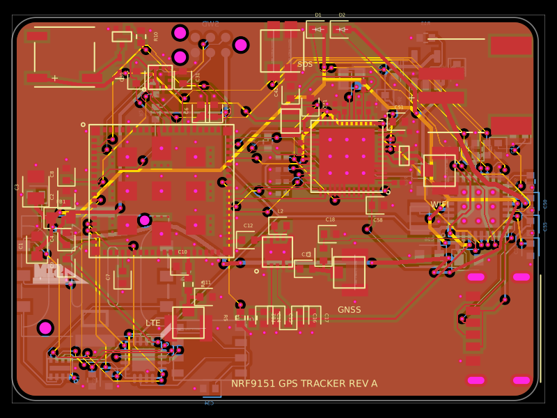 More from this authorpixalynx/nrf9151-gps-trackerA compact 44×32 mm, 4-layer nRF9151 LTE-M/NB-IoT/GNSS tracker PCB with nPM1300 LiPo/USB-C power, nano-SIM/eSIM switching, nRF7002 Wi‑Fi scanning, accelerometer, antennas, buzzer, LEDs, SOS button, and SWD/debug connectors.
 Similar packagegokul/usb-hub-boardA 4-layer 100×66 mm USB 2.0 hub board with a USB‑C upstream port, four protected downstream USB‑C/USB‑A ports, an integrated SD card reader, USB hub controllers, 3.3 V regulation, ESD protection, current-limited power switches, crystal oscillators, and filtering/passive components.
 Discover something newhrithik18k/smart-switch-pcbThe AO3400A component models a SOT-23 N-channel MOSFET with labeled pins for Gate, Source, and Drain, including 3D CAD models and schematic symbols for electronic circuit design.