pixalynx/usb3-hub-10g
A USB 3.2 Gen 2 six-port hub board with USB-C PD power input, regulated 5 V/3.3 V/1.15 V rails, one upstream and four protected downstream USB-A/USB-C ports, SuperSpeed muxes, ESD protection, and controlled port power.
- Version
- 0.0.1
- License
- unset
- Stars
- 0
parts/Connectors.tsx
import type { ChipProps } from "tscircuit"
import { JlcFootprint } from "../lib/jlc"
import { CAD } from "../lib/cad-models"

/** Receptacles. Footprints are JLC's (lib/jlc-footprints.json) with the mating face towards -y. Body extents come
 * from each part's EasyEDA 3D-model box (SVGNODE c_width/c_height/c_origin), in the footprint frame:
 *   USB-A GSB4111312HR   x +/-7.80, y -13.58..+3.02 (face at -13.58)
 *   USB-C 12401610E4#2A  x +/-5.25, y  -5.65..+3.55 (face at -5.65; SMT tails reach +4.28)
 *   USB-C TYPE-C-31-M-12 x +/-4.47, y  -5.05..+2.85 (face at -5.05; tails reach +3.12)
 * EDGE_Y is where the board edge goes (face overhangs it by ~0.5 mm, clear of the front shell-tab copper). */
export const EDGE_Y = { usba3: -13.05, usbc24: -5.15, usbc16: -4.55 } as const

/** Amphenol 12401610E4#2A, 24-contact USB-C receptacle rated USB 3.2 Gen 2. Pins 1-12 = A1-A12, 13-24 = B1-B12,
 * 25-28 = the four shell tabs (JLC C5119948 pads 14/15 twice). Signal names are the receptacle's (TX = the port
 * owner's transmitter). */
export const usbC24Pins = {
  pin1: ["GND_A1"], pin2: ["TX1P"], pin3: ["TX1N"], pin4: ["VBUS_A4"], pin5: ["CC1"], pin6: ["DP_A6"], pin7: ["DN_A7"], pin8: ["SBU1"],
  pin9: ["VBUS_A9"], pin10: ["RX2N"], pin11: ["RX2P"], pin12: ["GND_A12"],
  pin13: ["GND_B1"], pin14: ["TX2P"], pin15: ["TX2N"], pin16: ["VBUS_B4"], pin17: ["CC2"], pin18: ["DP_B6"], pin19: ["DN_B7"], pin20: ["SBU2"],
  pin21: ["VBUS_B9"], pin22: ["RX1N"], pin23: ["RX1P"], pin24: ["GND_B12"],
  pin25: ["SH1"], pin26: ["SH2"], pin27: ["SH3"], pin28: ["SH4"],
} as const
export const USBC24_GND = ["GND_A1", "GND_A12", "GND_B1", "GND_B12", "SH1", "SH2", "SH3", "SH4"] as const
export const USBC24_VBUS = ["VBUS_A4", "VBUS_A9", "VBUS_B4", "VBUS_B9"] as const
/** Contact order on the sheet: supplies, CC, USB 2.0, SuperSpeed lanes, SBU, then ground and shell (adjacent same-net
 * contacts share one label). `side` is the side the contacts are drawn on (towards the rest of the circuit). */
const USBC24_SCH = ["VBUS_A4", "VBUS_A9", "VBUS_B4", "VBUS_B9", "CC1", "CC2", "DP_A6", "DP_B6", "DN_A7", "DN_B7", "TX1P", "TX1N", "RX1P", "RX1N", "TX2P", "TX2N", "RX2P", "RX2N", "SBU1", "SBU2", ...USBC24_GND] as const
export const UsbC24 = ({ side, ...props }: ChipProps<typeof usbC24Pins> & { side: "left" | "right" }) => (
  <chip {...props} manufacturerPartNumber="12401610E4#2A" supplierPartNumbers={{ jlcpcb: ["C5119948"] }} pinLabels={usbC24Pins}
    footprint={<JlcFootprint part="usbc24" body={[-5.25, -5.65, 5.25, 4.3]} />} cadModel={CAD.usbc24} schWidth={1.4} schHeight={5.8}
    schPinArrangement={side === "right" ? { rightSide: { direction: "top-to-bottom", pins: [...USBC24_SCH] } } : { leftSide: { direction: "top-to-bottom", pins: [...USBC24_SCH] } }} />
)

/** HRO TYPE-C-31-M-12, 16-contact USB 2.0 receptacle for the power input (JLC C165948). The doubled VBUS and GND
 * contacts are single lands; 13-16 are the shell tabs. */
export const usbC16Pins = {
  pin1: ["GND1"], pin2: ["VBUS1"], pin3: ["CC1"], pin4: ["DP1"], pin5: ["DN1"], pin6: ["SBU1"], pin7: ["GND2"], pin8: ["VBUS2"], pin9: ["CC2"],
  pin10: ["DP2"], pin11: ["DN2"], pin12: ["SBU2"], pin13: ["SH1"], pin14: ["SH2"], pin15: ["SH3"], pin16: ["SH4"],
} as const
export const UsbC16 = (props: ChipProps<typeof usbC16Pins>) => (
  <chip {...props} manufacturerPartNumber="TYPE-C-31-M-12" supplierPartNumbers={{ jlcpcb: ["C165948"] }} pinLabels={usbC16Pins}
    footprint={<JlcFootprint part="usbc16" body={[-4.47, -5.05, 4.47, 3.2]} />} cadModel={CAD.usbc16} schWidth={1.2} schHeight={3.4}
    schPinArrangement={{
      rightSide: { direction: "top-to-bottom", pins: ["VBUS1", "VBUS2", "CC1", "CC2", "DP1", "DP2", "DN1", "DN2", "SBU1", "SBU2", "GND1", "GND2", "SH1", "SH2", "SH3", "SH4"] },
    }} />
)

/** Amphenol GSB4111312HR right-angle through-hole USB-A receptacle rated USB 3.2 Gen 2 (JLC C5429382). Pin 5/6 =
 * StdA_SSRX-/+ (the host's receiver), 8/9 = StdA_SSTX-/+; 10/11 shell legs. */
export const usbA3Pins = {
  pin1: ["VBUS"], pin2: ["DM"], pin3: ["DP"], pin4: ["GND"], pin5: ["SSRXN"], pin6: ["SSRXP"], pin7: ["GND_DRAIN"], pin8: ["SSTXN"], pin9: ["SSTXP"],
  pin10: ["SH1"], pin11: ["SH2"],
} as const
export const UsbA3 = (props: ChipProps<typeof usbA3Pins>) => (
  <chip {...props} manufacturerPartNumber="GSB4111312HR" supplierPartNumbers={{ jlcpcb: ["C5429382"] }} pinLabels={usbA3Pins}
    footprint={<JlcFootprint part="usba3" body={[-7.8, -13.58, 7.8, 3.02]} />} cadModel={CAD.usba3} schWidth={1.2} schHeight={2.4}
    schPinArrangement={{
      leftSide: { direction: "top-to-bottom", pins: ["VBUS", "DP", "DM", "SSTXP", "SSTXN", "SSRXP", "SSRXN", "GND", "GND_DRAIN", "SH1", "SH2"] },
    }} />
)

/** YXC X322525MOB4SI 25 MHz crystal, 12 pF load, 3225 (JLC Basic C9006): 1 OSC1, 2 GND, 3 OSC2, 4 GND. */
export const xtalPins = { pin1: ["OSC1"], pin2: ["GND2"], pin3: ["OSC2"], pin4: ["GND4"] } as const
export const Crystal25M = (props: ChipProps<typeof xtalPins>) => (
  <chip {...props} manufacturerPartNumber="X322525MOB4SI" supplierPartNumbers={{ jlcpcb: ["C9006"] }} pinLabels={xtalPins}
    footprint={<JlcFootprint part="xtal3225" />} cadModel={CAD.xtal3225} schWidth={1.2} schHeight={0.6}
    schPinArrangement={{ leftSide: { direction: "top-to-bottom", pins: ["OSC1", "GND2"] }, rightSide: { direction: "top-to-bottom", pins: ["OSC2", "GND4"] } }} />
)
Related Packages
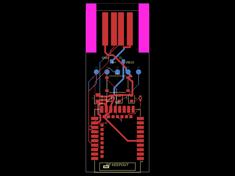 More from this authorpixalynx/keyboardThis code defines the physical layout and key components of a USB-C dongle featuring an nRF52840 microcontroller with antenna, USB-A connector, status LED, pair button, firmware debug test points, and associated passive components and interface connectors.
 Similar packagegokul/usb-hub-boardA 4-layer 100×66 mm USB 2.0 hub board with a USB‑C upstream port, four protected downstream USB‑C/USB‑A ports, an integrated SD card reader, USB hub controllers, 3.3 V regulation, ESD protection, current-limited power switches, crystal oscillators, and filtering/passive components.
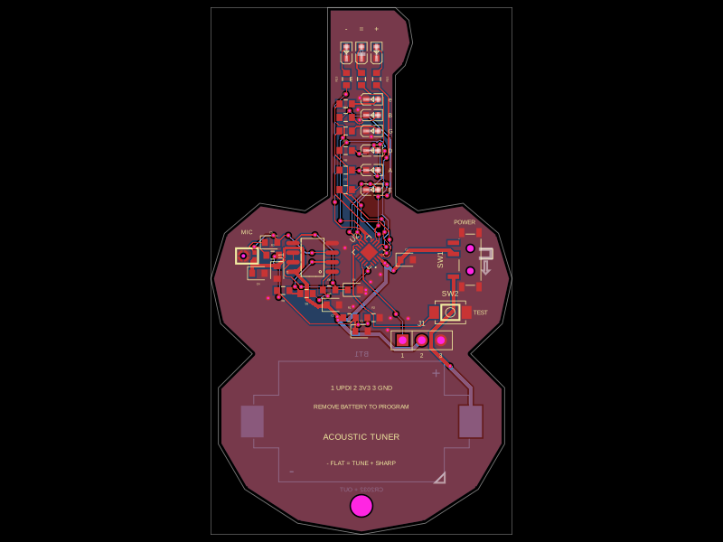 Discover something newgokul/acoustic-guitar-tunerThis code defines the physical pin configuration and footprint layouts for the ATtiny1616 microcontroller and a matching tactile switch component, including their key hardware connection points, dimensions, and 3D models.