pixalynx/usb3-hub-10g
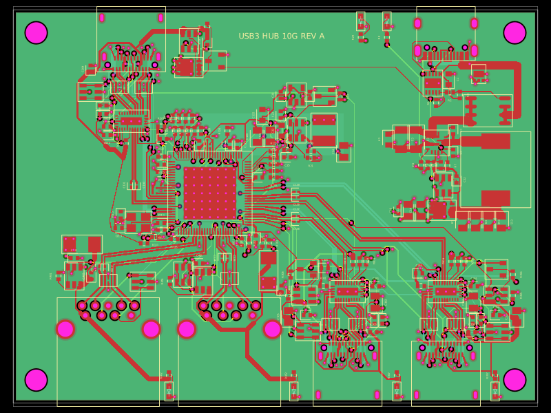
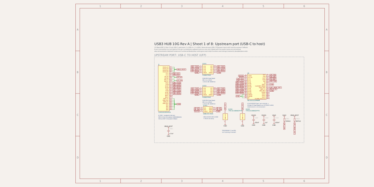
A USB 3.2 Gen 2 six-port hub board with USB-C PD power input, regulated 5 V/3.3 V/1.15 V rails, one upstream and four protected downstream USB-A/USB-C ports, SuperSpeed muxes, ESD protection, and controlled port power.
- Version
- 0.0.1
- License
- unset
- Stars
- 0
index.circuit.tsx
PCB
Schematic
import { Fragment } from "react"
import { Hub } from "./blocks/Hub"
import { TypeCPort } from "./blocks/TypeC"
import { TypeAPort } from "./blocks/TypeA"
import { PowerInput, Rails } from "./blocks/Power"
import { BOARD, SHEETS, SHEET_COUNT } from "./lib/layout"
import { RoutedTraces, type RoutedLegs } from "./lib/routed-traces"
import pairsJson from "./routing/pairs.json"
import meshJson from "./routing/mesh.json"
import powerJson from "./routing/power.json"
import routesJson from "./routing/index-routes.json"
import escapesJson from "./routing/escapes.json"
import { MeshCopper, type Mesh } from "./lib/mesh"
import flags from "./lib/flags.json"
import { SCHEMATIC_OFF } from "./lib/env"
import { SchLabels } from "./lib/sch-labels"
import { Sheet } from "./lib/sch"

/**
 * USB3 HUB 10G, Rev A: 10 Gbps (USB 3.2 Gen 2) 4-port hub. 80 x 60 mm, 6 layers (JLC06161H-7628), JLC PCBA.
 * Layers: top parts + TX pairs | inner1 GND | inner2 low-speed | inner3 VSYS5 plane | inner4 GND | bottom RX pairs.
 *
 * Back edge: USB-C to the host (J1, HD3SS3220 U2 as UFP) and USB-C PD power in (J2, HUSB238). Front edge: two
 * USB-A 3.x (J3/J4, hub ports 1-2, BC1.2) and two USB-C (J5/J6 via HD3SS3220 U3/U4 as DFP, 1.5 A).
 * Microchip USB7206C hub, strap-configured (no firmware). Per-port current-limited power switches controlled by
 * the hub (uhubctl). 5.1 V from a TPS56A37 buck on the PD input, with host-VBUS fallback through ideal diodes.
 *
 * Every value is sourced in docs/decisions.md and research/.
 */
const HOLE = { dx: BOARD.w / 2 - 3.5, dy: BOARD.h / 2 - 3.5 }

export default () => (
  <board width={`${BOARD.w}mm`} height={`${BOARD.h}mm`} thickness="1.6mm" layers={6} routingDisabled schematicDisabled={SCHEMATIC_OFF}
    pcbStyle={{ viaHoleDiameter: "0.3mm", viaPadDiameter: "0.5mm" }}>
    {/* one schematic sheet per block (lib/layout.ts SHEETS); PCB-wise these are plain containers */}
    <Sheet def={SHEETS.HUB} count={SHEET_COUNT}><Hub /></Sheet>
    <Sheet def={SHEETS.UP} count={SHEET_COUNT} legend><TypeCPort role="ufp" n={0} /></Sheet>
    <Sheet def={SHEETS.C1} count={SHEET_COUNT}><TypeCPort role="dfp" n={3} /></Sheet>
    <Sheet def={SHEETS.C2} count={SHEET_COUNT}><TypeCPort role="dfp" n={4} /></Sheet>
    <Sheet def={SHEETS.A1} count={SHEET_COUNT}><TypeAPort n={1} /></Sheet>
    <Sheet def={SHEETS.A2} count={SHEET_COUNT}><TypeAPort n={2} /></Sheet>
    <Sheet def={SHEETS.POWER} count={SHEET_COUNT}><PowerInput /></Sheet>
    {/* hand-planned SuperSpeed copper (scripts/pairs.py), routed copper, plane connections (scripts/mesh.py);
        "copper": false is only for schematic pre-passes (scripts/sch-eval.tsx --no-traces) */}
    {(flags as { copper?: boolean }).copper !== false && (
      <>
        <RoutedTraces routes={pairsJson as RoutedLegs} />
        <RoutedTraces routes={powerJson as RoutedLegs} />
        <RoutedTraces routes={escapesJson as RoutedLegs} />
        <RoutedTraces routes={routesJson as RoutedLegs} />
        <MeshCopper mesh={meshJson as unknown as Mesh} />
      </>
    )}
    <Sheet def={SHEETS.RAILS} count={SHEET_COUNT}><Rails /></Sheet>
    {/* schematic: net labels on every named-net pin (scripts/sch-labels.py) */}
    {!SCHEMATIC_OFF && (flags as { schLabels?: boolean }).schLabels !== false && <SchLabels />}
    {[[-1, -1], [1, -1], [-1, 1], [1, 1]].map(([sx, sy]) => (
      <Fragment key={`${sx}${sy}`}><hole pcbX={sx * HOLE.dx} pcbY={sy * HOLE.dy} diameter="3.2mm" /></Fragment>
    ))}
    <silkscreentext text="USB3 HUB 10G REV A" pcbX={1} pcbY={26} fontSize={1.2} />
    {flags.pours && (
      <>
      {/* planes: GND under each outer layer, VSYS5 in the middle */}
      <copperpour name="GND_L2" layer="inner1" connectsTo="net.GND" clearance={0.2} boardEdgeMargin={0.4} unbroken />
      <copperpour name="VSYS5_L4" layer="inner3" connectsTo="net.VSYS5" clearance={0.25} boardEdgeMargin={0.5} unbroken />
      <copperpour name="GND_L5" layer="inner4" connectsTo="net.GND" clearance={0.2} boardEdgeMargin={0.4} unbroken />
      {/* 1.15 V core island on the bottom under the hub, with a corridor to the TLV62569 output (L2 / C24 / C120-C121) */}
      <copperpour name="V1V15_L6" layer="bottom" connectsTo="net.V1V15" clearance={0.2}
        outline={[{ x: -16.2, y: -4.2 }, { x: -3.8, y: -4.2 }, { x: -3.8, y: 7.6 }, { x: 10.6, y: 7.6 }, { x: 10.6, y: 14.4 }, { x: -16.2, y: 14.4 }]} />
      </>
    )}
  </board>
)
Related Packages
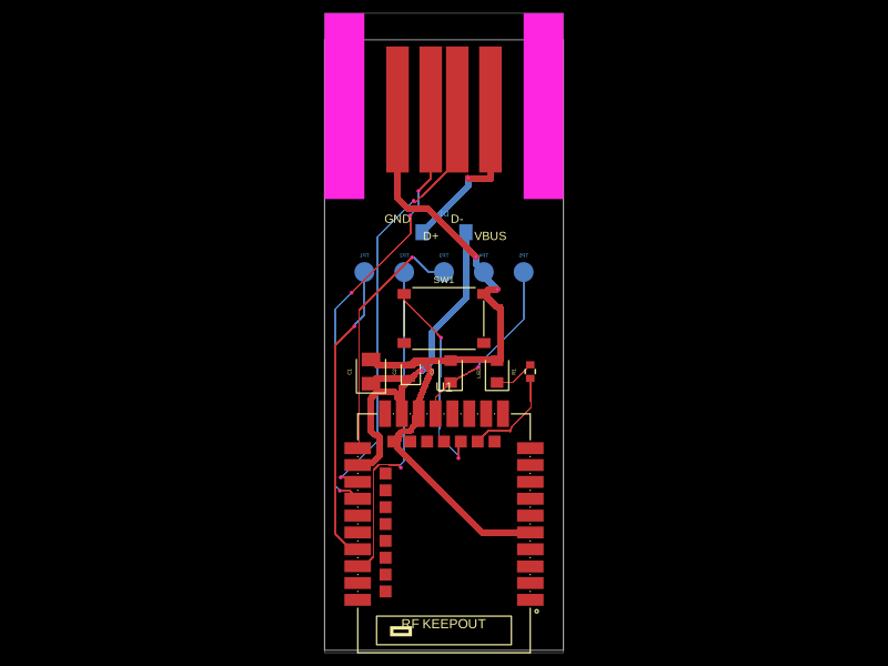 More from this authorpixalynx/keyboardThis code defines the physical layout and key components of a USB-C dongle featuring an nRF52840 microcontroller with antenna, USB-A connector, status LED, pair button, firmware debug test points, and associated passive components and interface connectors.
 Similar packagegokul/usb-hub-boardA 4-layer 100×66 mm USB 2.0 hub board with a USB‑C upstream port, four protected downstream USB‑C/USB‑A ports, an integrated SD card reader, USB hub controllers, 3.3 V regulation, ESD protection, current-limited power switches, crystal oscillators, and filtering/passive components.
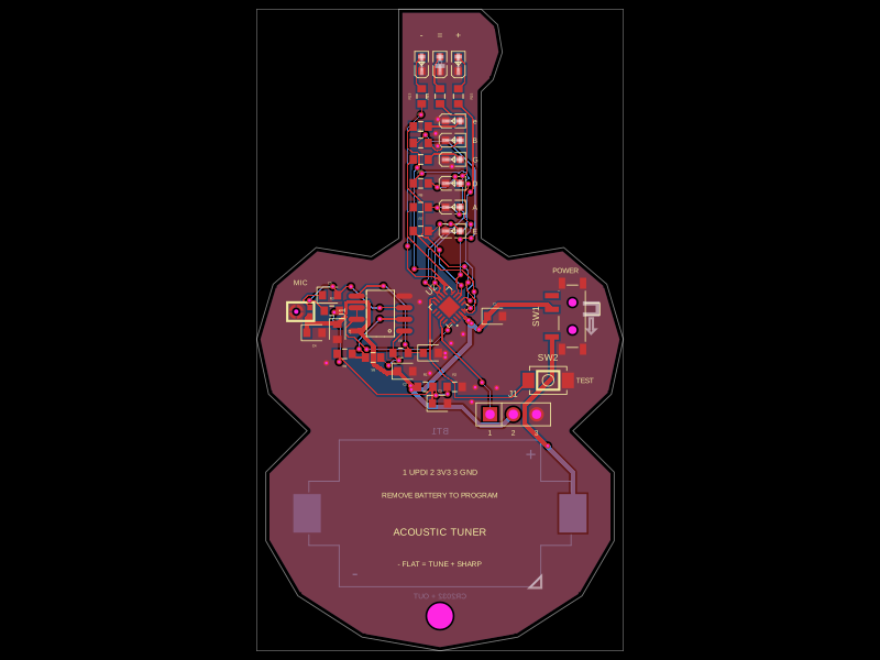 Discover something newgokul/acoustic-guitar-tunerThis code defines the physical pin configuration and footprint layouts for the ATtiny1616 microcontroller and a matching tactile switch component, including their key hardware connection points, dimensions, and 3D models.