pixalynx/usb3-hub-10g
A USB 3.2 Gen 2 six-port hub board with USB-C PD power input, regulated 5 V/3.3 V/1.15 V rails, one upstream and four protected downstream USB-A/USB-C ports, SuperSpeed muxes, ESD protection, and controlled port power.
- Version
- 0.0.1
- License
- unset
- Stars
- 0
fab/FAB-NOTES.md
# USB3 HUB 10G rev A: JLCPCB order notes

## PCB
| Option | Value |
|---|---|
| Layers | 6 |
| Stackup | **JLC06161H-7628**, impedance control ON |
| Material | FR-4 TG155 (JLC's impedance tables assume it) |
| Thickness | 1.6 mm |
| Outer / inner copper | 1 oz / 0.5 oz |
| Size | 80 x 60 mm |
| Min via | 0.3 mm drill / 0.5 mm pad (hub core and ESD ground: 0.2 / 0.35 mm) |
| Via covering | **Epoxy filled & capped** (via-in-pad on exposed pads, MOSFET tabs and ESD ground pins) |
| Surface finish | **ENIG** (user choice 2026-09-30: 0.4-0.5 mm pitch QFNs, via-in-pad) |
| Min trace / space | 0.15 / 0.1 mm (SuperSpeed 0.27 / 0.13 mm) |

Controlled impedance: 90 ohm differential on L1 and L6. Traces are 0.27 mm wide with a 0.13 mm gap, referenced to the L2 and L5 GND planes.
The stackup's dielectrics: L1-L2 and L5-L6 are 210.4 um 7628 prepreg.

## Layers
| Layer | Use |
|---|---|
| L1 | Parts, SuperSpeed TX, breakouts, power copper |
| L2 | GND plane |
| L3 | Signals |
| L4 | 5 V (VSYS5) plane |
| L5 | GND plane |
| L6 | SuperSpeed RX, 1.15 V island under the hub |

## Assembly
- **Sides.** Top side only.
- **Footprints.** Every IC and connector uses JLC's own EasyEDA land pattern. The CPL rotation and position are fitted to JLC's library footprint (scripts/check-jlc-footprints.py): 56 parts checked, 0 flagged.
- **Check in the SMT preview:**
  - U1 USB7206CT/KDX (C3210691) has no EasyEDA footprint. Its pattern is taken from C3210686 (the same VQFN-100 package), so check the pin-1 dot.
  - The white LEDs (C2290): check cathode orientation.
  - The 220 uF polymer capacitors C402 and C452: check polarity.
- **Stock.** USB7206CT/KDX stock is thin (21 at JLC on 2026-09-28). Pre-order it or reserve it before placing the order.
Related Packages
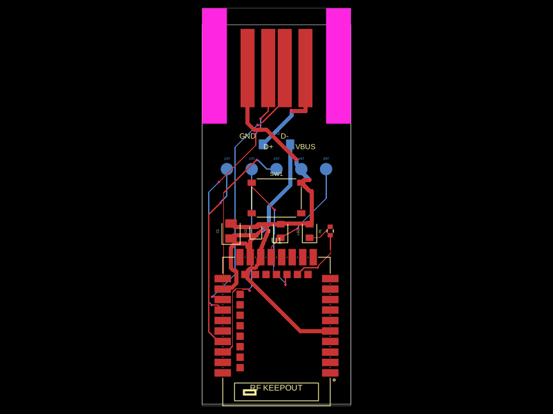 More from this authorpixalynx/keyboardThis code defines the physical layout and key components of a USB-C dongle featuring an nRF52840 microcontroller with antenna, USB-A connector, status LED, pair button, firmware debug test points, and associated passive components and interface connectors.
 Similar packagegokul/usb-hub-boardA 4-layer 100×66 mm USB 2.0 hub board with a USB‑C upstream port, four protected downstream USB‑C/USB‑A ports, an integrated SD card reader, USB hub controllers, 3.3 V regulation, ESD protection, current-limited power switches, crystal oscillators, and filtering/passive components.
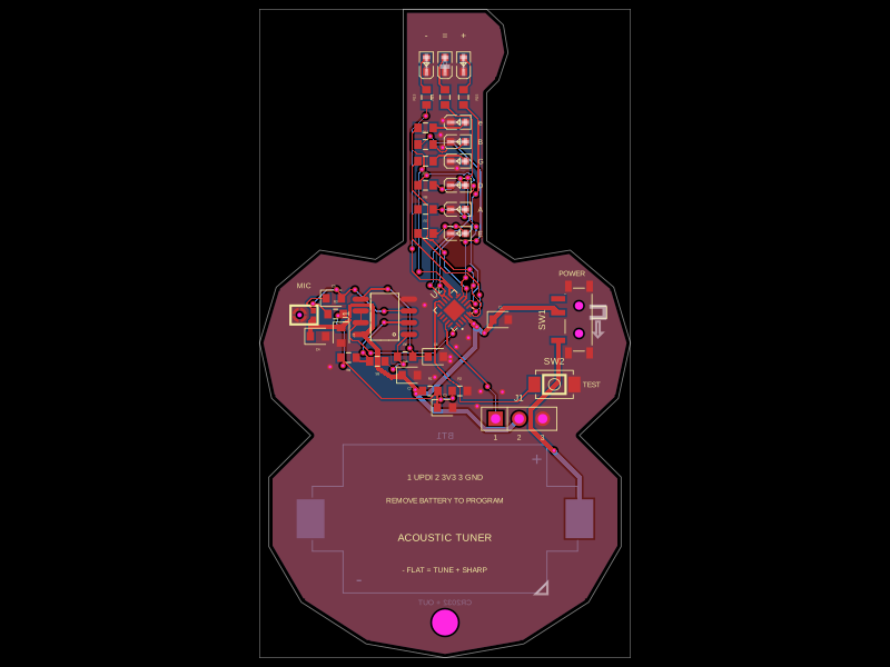 Discover something newgokul/acoustic-guitar-tunerThis code defines the physical pin configuration and footprint layouts for the ATtiny1616 microcontroller and a matching tactile switch component, including their key hardware connection points, dimensions, and 3D models.