pixalynx/usb3-hub-10g
A USB 3.2 Gen 2 six-port hub board with USB-C PD power input, regulated 5 V/3.3 V/1.15 V rails, one upstream and four protected downstream USB-A/USB-C ports, SuperSpeed muxes, ESD protection, and controlled port power.
- Version
- 0.0.1
- License
- unset
- Stars
- 0
docs/decisions.md
# USB3 HUB 10G: decisions

Started 2026-09-28 as an interactive session. The user picked each option; I did the research and the implementation.

## User choices

| Topic | Choice |
|---|---|
| Link speed | 10 Gbps (USB 3.2 Gen 2) |
| Upstream connector | USB-C receptacle |
| Power | Separate USB-C PD input, falling back to host bus power when no charger is plugged in |
| USB-C downstream power | 5 V, 1.5 A advertised (Rp only, no PD source) |
| USB-A ports | Two single right-angle receptacles, BC1.2 charging |
| Form factor | Desktop box: host and power on the back edge, 4 ports on the front |
| Extras | Per-port power switching (uhubctl), status LEDs, enclosure mounting holes |
| Hub | Microchip USB7206C plus 3x TI HD3SS3220 |
| Quantity | 2-5 prototypes, JLC PCBA |
| PD sink | HUSB238 |
| LEDs | White (JLC Basic) |
| Charger | 45-65 W laptop charger |
| Front port order | A A C C (left to right) |
| Spacing | Standard, 80 x 60 mm board |
| Assembly | Top side only |

## Why these parts

- **USB7206CT/KDX (C3210691).** It is the only Gen 2 hub whose datasheet, checklist and eval-board schematic are public, that JLC stocks (21 on 2026-09-28), and that needs no firmware, since straps configure it.
  - VL822 and GL3590 have NDA-only datasheets and zero stock.
  - RTS5420 is in stock, but its datasheet is under NDA.
  - USB7216C defaults to a 3 A Type-C advertisement, which only per-board OTP can change.
  - The industrial -I/KDX variant (C3210686) is effectively sold out (presale -1).
  - The CT variant has no EasyEDA entry; its land pattern is taken from C3210686, which has the same package.
- **HD3SS3220 (C165155).** A 10 Gbps 2:1 mux, CC logic and VCONN in one chip, configured entirely by pins.
  - The USB7206C has no Type-C support at all: no CC pins, one SuperSpeed pair per port (DS00003850F; checklist DS00003336).
  - TUSB320-class chips report orientation only over I2C, or advertise only default current in GPIO mode.
- **HUSB238_002DD.** Two resistors configure it:
  - VSET open requests up to 20 V; ISET 13.7k requests 2.25 A.
  - From the charger's offers it picks the highest voltage that also has enough current. The `_002` variant tries the next lower offer instead of dropping straight to 5 V.
  - STUSB4500 would need NVM programming first.
- **TPS56A37 buck.** 10 A, runs from 4.5-28 V, reaches 98 % duty (so it still works on 5 V-only chargers), has power-good and output discharge. It follows TI's 5 V reference (Figure 7-1) with RFBT 75k, giving 5.1 V.
- **Power budget.** 4 ports x 1.5 A x 5.1 V is about 31 W, plus the hub (about 1.3 W core, 0.3 W I/O) and losses: about 36 W worst case.

## Power path and the bus-power fallback

- **Two ideal-diode legs into VSYS5.** V5_PD (the buck output) and VBUS_HOST each feed VSYS5 through an LM74700 driving a CSD17578Q3A N-FET.
  - The host leg's EN is pulled low by a 2N7002 whenever the buck's PG is high. So with a charger present, the hub never draws from the computer and never back-feeds it: USB hosts may run at 5.25 V, which would outrank a 5.1 V buck in a plain diode-OR.
- **PG pull-up trap.** The buck's PG is pulled up to V5_PD itself.
  - TPS56A37 leaves PG high-impedance when VIN < 2 V (Table 6-1), so a pull-up to VSYS5 would read "good" with no charger and lock the host leg off.
  - With no charger, V5_PD is 0 V because the PD-leg FET blocks back-feed, so PG reads low.
- **Handover.** When the charger is unplugged, the host FET's body diode carries VSYS5 at about -0.7 V until its LM74700 enables (about 75 us).
- **Fallback limits.** In fallback the downstream ports are limited by what the host port can supply. The hub still describes itself as self-powered, which is a USB-spec deviation accepted for a DIY hub.

## Sequencing

- **Rail order.** VSYS5 first, then TLV75733P 3.3 V. The TLV62569P 1.15 V core has EN tied to 3.3 V, so VCORE rises after VDD33 (DS00003850F 9.6.1).
- **Reset.** Core PG goes through a 10k/1 uF RC to become HUB_RESET_N.
- **HD3SS3220 enable.** HUB_RESET_N drives a 2N7002 that pulls the shared EN_CC_N low.
  - All three HD3SS3220s pull DIR up to 3.3 V, which is a supply other than VDD5, so ENn_CC must stay high until both supplies are stable (SLLSES1E 6.3.12, Figure 6-3).
  - In shutdown the chip keeps its dead-battery Rd (6.4.4), so the host keeps VBUS on during start-up. This makes the bus-power fallback safe.

## Port power (uhubctl)

- **USB-A ports.** AP22653 with EN and FAULT_N both on PRT_CTLx, as in DS00003850F Figure 8-2. RLIM 15k gives 1.735 A (±7 %), enough for BC1.2 CDP at 1.5 A. Each port has 220 uF polymer bulk; USB requires 120 uF per Type-A port.
- **USB-C ports.** AP22652 with an active-low EN. Its EN_N is pulled up and is pulled low only through a 2N7002 with:
  - gate on PRT_CTLx (the hub enables the port);
  - source on the HD3SS3220's ID (a device is attached, and ID asserts only once VBUS is at vSafe0V).
- **Why this gating.** PRT_CTLx sees only a MOSFET gate, so an idle port never reads as an over-current. FAULT_N still reaches PRT_CTLx. The switch discharges VBUS when disabled, which Type-C requires.
- **Hub straps.** CFG_BC_EN 10k pull-down puts BC1.2 on ports 1-2 (the USB-A ports). CFG_NON_REM 200k pull-down makes every port removable. Ports 5 and 6 are disabled by tying their D+/D- to 3.3 V.

## Values changed from the references

- **Hub VBUS_DET divider.** 100k/120k (2.73 V at 5 V) instead of Microchip's 43k/49.9k: Basic parts, same function.
- **Core feedback.** 22k/24k, giving exactly 1.150 V.
- **HD3SS3220 VBUS_DET.** 887k: TI specifies 880-910k and 900k is not an E-series value.
- **CURRENT_MODE.** 499k (TI says 500k).
- **Crystal.** YXC X322525MOB4SI (Basic, 12 pF load) with 18 pF load caps: 12 pF x 2 minus about 5 pF of pin and stray capacitance.

## Layout

- **Hub orientation.** USB7206C rotated 90° CCW. DN1/DN2 exit towards the USB-A ports at the front, DN3/DN4 towards the USB-C side, and UP towards the host receptacle at the back-left.
- **Footprints.** Every IC and connector land pattern is JLC's own EasyEDA pattern (`scripts/gen-jlc-footprints.py`), so the CPL rotation equals pcbRotation.
- **JLC data fix.** The Amphenol 12401610E4#2A entry is missing one of its two NPTH pegs; it was re-added from the KiCad and manufacturer data.

## Stackup (user choice, 2026-09-29): 6 layers, JLC06161H-7628

Once the 22 SuperSpeed pairs were routed on 4 layers, the pairs formed walls on both outer layers between the power
section and the four port switches, and both inner layers were GND. The user chose 6 layers over (a) a 4-layer board
with a 5 V inner plane as the bottom-layer pairs' reference, or (b) hand-routed 5 V hopping between layers.

| Layer | Use |
|---|---|
| L1 top | parts, TX pairs, receptacle breakouts |
| L2 inner1 | GND plane (reference for L1) |
| L3 inner2 | low-speed signals, 1.15 V island under the hub |
| L4 inner3 | VSYS5 (5 V) plane |
| L5 inner4 | GND plane (reference for L6) |
| L6 bottom | RX pairs, B-row escapes, low-speed |

JLC06161H-7628 dielectrics: L1-L2 and L5-L6 are 210.4 um 7628 prepreg (er 4.4), L2-L3 and L4-L5 are 400 um cores (er 4.6), L3-L4 is 202.8 um 7628.
The outer dielectric is the same as JLC04161H-7628's, so the pair geometry is unchanged: 0.27 mm traces with a 0.13 mm gap
(0.40 mm pitch) give 90.1 ohm on L1 and on L6 (scripts/zdiff.py, 2D field solver: within ~1.5 ohm of Hammerstad-Jensen for
a single line, ~2 ohm grid convergence). Order with impedance control and FR-4 TG155 (JLC's impedance tables assume it).

## Lane polarity (by design)

Two chips with counter-clockwise pin numbering, facing each other, see each other's pins mirrored, so pairs
routed without crossovers arrive P/N-swapped. Every USB 3.x receiver must detect and correct lane polarity
inversion, so the netlist deliberately swaps:
- the system side of all three HD3SS3220s (TX and RX), and
- the receptacle side's TX1 and RX1 lanes on all three USB-C ports (blocks/TypeC.tsx).
USB 2.0 D+/D- are never swapped.

## Power-stage layout (2026-09-29)

The first placement put the inductor's switch pad on the far side from the buck, which gave about 11 mm of switch node and
10 mm from the inductor to the output caps. The block was re-placed along TI's layout guidelines (SLVSHC9 7.4.1):
- **Buck.** U6 stays where it was. Its VIN pad is fed from the north and its PGND pad from the west.
- **Input caps.** C3, C2 and C4 stand upright west of U6, with the GND pin south. C3's GND pin also connects straight to PGND on the top layer.
- **Inductor.** L1 is rotated 270°, so its switch pad faces U6.SW.
  - The switch-node copper is 1.0 mm wide from just east of the pad (it passes between the BOOT and SS pads), then 1.6 mm to the inductor.
  - BOOT cap C6 sits above that copper.
- **5 V output.** The 5 V pad feeds a 1.8 mm bus straight into the Q2 sources. The four 22 uF output caps hang under the bus.
  - Q2's drain tab carries VSYS5 into the L4 plane through in-pad vias.
  - The LM74700 sits above Q2, with its GATE and ANODE pins facing it.
- **Feedback.** The FB/PG/MODE resistors sit in one row under U6. The top feedback resistor has its own 5 V sense trace (guideline 9).
- **Charger input.** A 1.2 mm bus runs from J2.VBUS1 over the TVS IN pins and down the right edge to Q1's sources.
  - J2.VBUS2 joins it through a bottom-layer bridge, so all four VBUS contacts share the current.
  - Q1's drains feed a 1.2 mm bus to U6.VIN.
- **HUSB238.** Rotated 180°, so its CC, D+/D- and VIN row faces the connector.
- **IHLP-4040 courtyard.** JLC's pattern only covers the pads; the courtyard now matches the real 10.2 x 10.2 mm body.

All of this copper is hand-laid in `scripts/power.py` and audited together with the SuperSpeed pairs (0 findings).
Freerouting routes only the low-current leftovers of these nets.

## Routing round 1 fixes (2026-09-29)

The first Freerouting pass left about 20 connections open. Every one traced back to placement or to plane vias,
so these were fixed before re-routing:
- **HD3SS3220 straps (U3/U4).** The VBUS_DET, PORT and CURRENT_MODE resistors are turned so their strap pad faces the mux. They moved to y -8.4, which leaves room for a 45° fan-out from the 0.4 mm-pitch row.
- **Mux escapes.** CC1/CC2, ENn_CC and ID escape through staggered vias; the U3/U4 VDD5 caps and U4's port switch moved out of that area.
  - VCC33 sits between the RX and TX pairs, so it runs up between them to a via above the RX layer-change vias.
  - GND28 (and U2's PORT, which is GND on the upstream mux) ties inward to the exposed pad. Their plane vias had blocked the neighbouring pins.
  - All of this is in `scripts/escapes.py`.
- **Crystal.** Y1 moved from 7.5 mm to about 3 mm from the hub.
  - XTALO runs straight out. XTALI runs under the can between the pad rows.
  - The 18 pF load caps sit on the far side of the can.
- **VCORE_78 / VDD33_79 caps.** The placement nudge had the wrong sign on the hub's left side, so the two caps were swapped relative to their pins.
- **V1V15 island.** Vias for the 1.15 V pour are now confined to the bottom-layer island. Three had landed outside it.
- **ESD array ground pins.** The GND pins of the upstream ESD arrays (boxed in by pairs) take a 0.2/0.35 mm via-in-pad.
- **Alignment pegs.** Four bottom-layer SuperSpeed runs crossed USB-C alignment-peg holes. They now pass inside the pegs with ≥0.19 mm clearance, and the pair audit checks NPTH holes.

## Routing completion (2026-09-30)

- **Pull-down array.** The hub's TEST1-3 10k pull-ups and pin 62's decoupler are now 0201s staggered at their pins, like the in-lane VCORE caps. The 0402 decoupler in front of TEST1 had boxed in the three TEST leads.
  - SPI_D3's pull-down is reached up the 0.36 mm column gap in the array.
- **Freerouting.** 16 passes route everything except 2-3 connections, and which ones stay open changes whenever fixed copper changes. Those were closed with the multi-layer maze router and are kept as fixed copper in `routing/maze-fixed.json`:
  - R110 to the VBUS_HOST net and to R111;
  - C2's CC2 through its ESD diode;
  - one J6 VBUS pin;
  - the parked-DN5 V3V3 cluster to C203.
- **Port VBUS copper.** It is routed at 0.25 mm so it can leave the 0.5 mm-pitch connector pins. `scripts/widen.py --overlay` then lays 0.7 mm copper along each path from its wide end, up to the necks.
- **Verification** (pours on: GND L2/L5, VSYS5 L4, 1.15 V island L6; each is one unbroken island):
  - build: 0 errors;
  - physical connectivity: 161/161 nets;
  - clearance: 0 findings at 0.1 mm, including via-in-pour and trace-in-pour shorts and drill spacing.
- **Fab package** (`scripts/export-fab.py` → `fab/`):
  - every via normalised to L1-L6: 482 through vias, one drill file;
  - JLC BOM (56 lines) and CPL (191 parts, top only);
  - CPL rotations and origins fitted to JLC's footprints: 0 flags, with U1 to be checked in the SMT preview;
  - order options are in `fab/FAB-NOTES.md`.

## Schematic (2026-09-30)

- **Sheets.** Eight sheets, in signal-flow order:
  1. Upstream port
  2. Hub
  3. USB-A port 1
  4. USB-A port 2
  5. USB-C port 1
  6. USB-C port 2
  7. Power input, 5.1 V buck, OR-ing
  8. 3.3 V / 1.15 V rails and reset
  - Each sheet has a zoned border and a title line, and sheet 1 carries the legend. Every chip has a note with its function and datasheet ratings (from `research/*.txt`).
  - Why eight sheets: `tsci check schematic-placement` wants every decoupling cap of a rail to be within 4 units of the others on the same sheet. On one sheet that was impossible, with 13 caps on V3V3 and 16 on VSYS5.
  - On each sheet each rail's caps now form one group:
    - hub: V1V15 in a 4 x 2 group, V3V3 in 3 x 3;
    - USB-C sheets: the switch input cap joins the HD3SS3220's VSYS5 caps;
    - rails sheet: U9's input cap joins U10's.
  - The check reports no issues on the entry file, on a fresh evaluation and on the build.
- **Parts name their sheet (`schSheetName`); they are not children of `<schematicsheet>`.** Core auto-lays-out a sheet's children and ignores schX/schY.
  - `lib/layout.ts` maps each schematic section to its sheet (`onSheet`).
  - Notes and frames take the sheet from the enclosing `<Sheet>` (`lib/sch.tsx`).
  - Each generated net label carries the sheet of its part.
- **Net labels, no wires.** Every pin on a named net carries a label generated by `scripts/sch-labels.py` into `lib/sch-labels.json`. Adjacent pins on one net share a single label through a comb. Labels with the same name connect across sheets.
  - The only solver wires are the 0.1 lead-ins from each LED to its series resistor.
  - Nets that used to be unnamed port-to-port links now have names:
    - the hub's straps and unused-function pull-downs, named after the hub pin (CFG_STRAP1, SPI_CLK, DN5_RXP, ...);
    - BUCK_SS, BUCK_MODE, BUCK_BOOT, BUCK_FB, CORE_FB, HUSB_GATE, PD_ISET;
    - *_VBUS_DET, *_PORT, *_CUR_MODE, *_ILIM, PDOR_VCAP, HOSTOR_VCAP.
  - Connectivity is unchanged: `scripts/pcb-diff.py` shows the PCB identical to the pre-schematic build, and 161/161 nets are joined.
- **Build time.** The schematic used to take 13-16 minutes of every build. Almost all of it was tscircuit's inline net-label phase, triggered by the routed PCB legs' trace names.
  - The legs are now named only in schematic-off builds (`lib/routed-traces.tsx`). The routing tools that look legs up by name need `lib/flags.json` "schematic": false.
  - A full build with pours and schematic takes under a minute.
- **Editing.** Move parts in `blocks/*.tsx` (block origins and sheets are in `lib/layout.ts`), then run `./scripts/sch-cycle.sh`, which takes about a minute. It:
  - regenerates the labels;
  - renders each sheet to `.tmp/sch-view-<n>-<sheet>.png`;
  - runs the overlap check (`scripts/sch-overlaps.py`) on each sheet and `tsci check schematic-placement`;
  - exits 1 on any finding.
  - `tsci check schematic-placement` exits 0 even when it lists issues. Judge it by its output: clean means no issue lines.
Related Packages
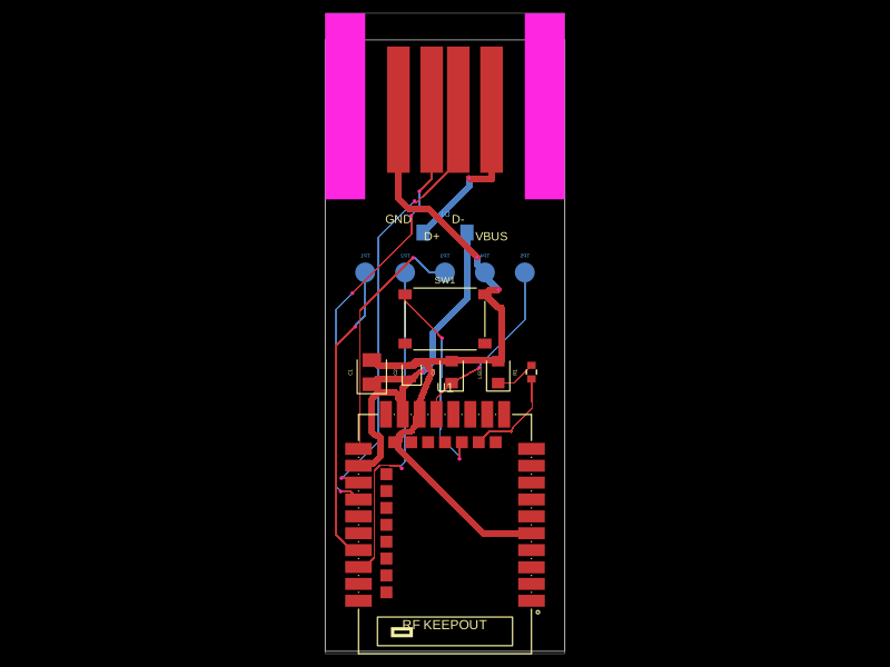 More from this authorpixalynx/keyboardThis code defines the physical layout and key components of a USB-C dongle featuring an nRF52840 microcontroller with antenna, USB-A connector, status LED, pair button, firmware debug test points, and associated passive components and interface connectors.
 Similar packagegokul/usb-hub-boardA 4-layer 100×66 mm USB 2.0 hub board with a USB‑C upstream port, four protected downstream USB‑C/USB‑A ports, an integrated SD card reader, USB hub controllers, 3.3 V regulation, ESD protection, current-limited power switches, crystal oscillators, and filtering/passive components.
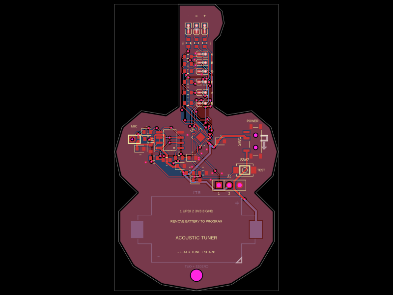 Discover something newgokul/acoustic-guitar-tunerThis code defines the physical pin configuration and footprint layouts for the ATtiny1616 microcontroller and a matching tactile switch component, including their key hardware connection points, dimensions, and 3D models.