pixalynx/usb3-hub-10g
A USB 3.2 Gen 2 six-port hub board with USB-C PD power input, regulated 5 V/3.3 V/1.15 V rails, one upstream and four protected downstream USB-A/USB-C ports, SuperSpeed muxes, ESD protection, and controlled port power.
- Version
- 0.0.1
- License
- unset
- Stars
- 0
blocks/Power.tsx
import { pcb } from "../lib/place"
import { UsbC16 } from "../parts/Connectors"
import { Husb238, Tps56a37, Lm74700, Csd17578, Ao4407a, Tlv75733, Tlv62569, Nmos } from "../parts/Power"
import { Tvs2200 } from "../parts/Protection"
import { R, C, L, Led } from "../lib/passives"
import { J, HUB, S, onSheet } from "../lib/layout"
import { Note, Frame } from "../lib/sch"

/** Power tree (docs/decisions.md):
 *   J2 USB-C PD in -> HUSB238 (VSET open = 20 V max, ISET 13.7k = 2.25 A) -> AO4407A -> VIN_BUCK
 *   -> TPS56A37 5.1 V (TI Figure 7-1 values, RFBT 75k) -> V5_PD -> LM74700 + CSD17578 ideal diode -> VSYS5
 *   host VBUS -> LM74700 + CSD17578 ideal diode -> VSYS5, held off (EN low) while the buck reports power-good.
 * The buck PG is pulled up to its own output: with no charger V5_PD is 0 V (the PD-leg FET blocks back-feed), so PG
 * reads low even though the TPS56A37 leaves PG high-impedance below VIN 2 V (datasheet Table 6-1). On a charger
 * unplug the host FET's body diode carries VSYS5 until its LM74700 enables (~75 us).
 *   VSYS5 -> TLV75733P 3.3 V -> TLV62569P 1.15 V (EN = 3.3 V, so VCORE follows VDD33 per DS00003850F 9.6.1)
 *   core PG -> 10k/1 uF -> HUB_RESET_N; HUB_RESET_N high -> 2N7002 pulls EN_CC_N low: every HD3SS3220 leaves
 *   shutdown (Rd kept) only after both of its supplies are stable (SLLSES1E 6.3.12, Figure 6-3). */
const pd = (dx: number, dy: number) => ({ x: J.PWR.x + dx, y: J.PWR.y + dy })
const rl = (dx: number, dy: number) => ({ x: HUB.x + dx, y: HUB.y + dy })
/** Schematic helpers per block: passive placement (sx/sy/sec), chip placement (schX/schY/section) and notes. */
const blk = (sec: "PD" | "BUCK" | "ORING" | "RAILS") => {
  const [ox, oy] = S[sec]
  return {
    p: (dx: number, dy: number) => ({ sx: ox + dx, sy: oy + dy, sec }),
    c: (dx: number, dy: number) => ({ schX: ox + dx, schY: oy + dy, schSectionName: sec, ...onSheet(sec) }),
    n: (dx: number, dy: number, lines: string[]) => <Note x={ox + dx} y={oy + dy} lines={lines} />,
    f: (x0: number, y0: number, x1: number, y1: number, title: string) => <Frame x0={ox + x0} y0={oy + y0} x1={ox + x1} y1={oy + y1} title={title} />,
  }
}
const PD = blk("PD"), BK = blk("BUCK"), OR = blk("ORING"), RL = blk("RAILS")

export const PowerInput = () => (
  <>
    <UsbC16 name="J2" {...pcb("J2", { x: J.PWR.x, y: J.PWR.y, rot: J.PWR.rot })} {...PD.c(0, 0)} />
    {["VBUS1", "VBUS2"].map((p) => <trace key={p} from={`J2.${p}`} to="net.VBUS_PD" />)}
    {["GND1", "GND2", "SH1", "SH2", "SH3", "SH4"].map((p) => <trace key={p} from={`J2.${p}`} to="net.GND" />)}
    <trace from="J2.CC1" to="net.PD_CC1" /><trace from="J2.CC2" to="net.PD_CC2" />
    <trace from="J2.DP1" to="net.PD_DP" /><trace from="J2.DP2" to="net.PD_DP" />
    <trace from="J2.DN1" to="net.PD_DM" /><trace from="J2.DN2" to="net.PD_DM" />

    <Tvs2200 name="D1" {...pcb("D1", { x: J.PWR.x - 5, y: J.PWR.y - 5 })} {...PD.c(3.6, 0.2)} />
    {["IN4", "IN5", "IN6"].map((p) => <trace key={p} from={`D1.${p}`} to="net.VBUS_PD" />)}
    {["GND1", "GND2", "GND3", "EP"].map((p) => <trace key={p} from={`D1.${p}`} to="net.GND" />)}

    <Husb238 name="U5" {...pcb("U5", { x: J.PWR.x, y: J.PWR.y - 9 })} {...PD.c(8.2, 0.2)} />
    <trace from="U5.VIN" to="net.VBUS_PD" /><trace from="U5.GND" to="net.GND" />
    <trace from="U5.CC1" to="net.PD_CC1" /><trace from="U5.CC2" to="net.PD_CC2" />
    <trace from="U5.DP" to="net.PD_DP" /><trace from="U5.DM" to="net.PD_DM" />
    <trace from="U5.ISET" to="net.PD_ISET" /><trace from="U5.GATE" to="net.HUSB_GATE" />
    <C name="C1" v="1uF" fp="0603" volts={50} a="VBUS_PD" b="GND" {...pd(-3, -8)} {...PD.p(7.0, -3.4)} />
    <R name="R1" v="13.7k" a="PD_ISET" b="GND" {...pd(3, -8)} {...PD.p(10.0, -3.4)} />
    <R name="R2" v="5.1k" a="HUSB_GATE" b="PD_GATE" {...pd(3, -10)} {...PD.p(11.3, -3.4)} />
    <R name="R3" v="49.9k" a="VBUS_PD" b="PD_GATE" {...pd(5, -10)} {...PD.p(12.6, -3.4)} />
    <Ao4407a name="Q1" {...pcb("Q1", { x: J.PWR.x + 6, y: J.PWR.y - 14, rot: 90 })} {...PD.c(14.6, 0.2)} />
    {["S1", "S2", "S3"].map((p) => <trace key={p} from={`Q1.${p}`} to="net.VBUS_PD" />)}
    {["D5", "D6", "D7", "D8"].map((p) => <trace key={p} from={`Q1.${p}`} to="net.VIN_BUCK" />)}
    <trace from="Q1.G" to="net.PD_GATE" />

    {/* 5.1 V buck */}
    <Tps56a37 name="U6" {...pcb("U6", { x: J.PWR.x - 4, y: J.PWR.y - 20 })} {...BK.c(0, 0)} />
    <trace from="U6.VIN" to="net.VIN_BUCK" /><trace from="U6.AGND" to="net.GND" /><trace from="U6.PGND" to="net.GND" />
    <trace from="U6.SW" to="net.BUCK_SW" /><trace from="U6.PG" to="net.BUCK_PG" />
    <trace from="U6.SS" to="net.BUCK_SS" /><trace from="U6.MODE" to="net.BUCK_MODE" />
    <trace from="U6.BOOT" to="net.BUCK_BOOT" /><trace from="U6.FB" to="net.BUCK_FB" />
    <C name="C2" v="10uF" fp="1206" volts={50} jlc="C13585" a="VIN_BUCK" b="GND" {...pd(-8, -17)} {...BK.p(-3.4, -3.4)} />
    <C name="C3" v="10uF" fp="1206" volts={50} jlc="C13585" a="VIN_BUCK" b="GND" {...pd(-8, -20)} {...BK.p(-2.1, -3.4)} />
    <C name="C4" v="100nF" fp="0603" volts={50} a="VIN_BUCK" b="GND" {...pd(-6, -18)} {...BK.p(-0.8, -3.4)} />
    <C name="C5" v="47nF" a="BUCK_SS" b="GND" {...pd(-6, -23)} {...BK.p(0.5, -3.4)} />
    <R name="R4" v="52.3k" a="BUCK_MODE" b="GND" {...pd(-7, -23)} {...BK.p(1.8, -3.4)} />
    <C name="C6" v="100nF" a="BUCK_BOOT" b="BUCK_SW" {...pd(-2, -18)} {...BK.p(3.1, -3.4)} />
    <L name="L1" v="3.3uH" part="ihlp4040" mpn="IHLP4040DZER3R3M01" jlc="C845075" a="BUCK_SW" b="V5_PD" {...pd(4, -23)} {...BK.p(5.2, 0.4)} />
    <R name="R5" v="75k" a="V5_PD" b="BUCK_FB" {...pd(-2, -23)} {...BK.p(4.4, -3.4)} />
    <R name="R6" v="10k" a="BUCK_FB" b="GND" {...pd(-2, -24.5)} {...BK.p(5.7, -3.4)} />
    <C name="C7" v="150pF" a="V5_PD" b="BUCK_FB" {...pd(-3.5, -24.5)} {...BK.p(7.0, -3.4)} />
    <R name="R7" v="100k" a="V5_PD" b="BUCK_PG" {...pd(-4, -26)} {...BK.p(8.3, -3.4)} />
    {[0, 1, 2, 3].map((i) => <C key={i} name={`C${8 + i}`} v="22uF" fp="0805" a="V5_PD" b="GND" {...pd(9, -19 - i * 2)} {...BK.p(9.6 + i * 1.3, -3.4)} />)}

    {/* PD leg ideal diode (always enabled) */}
    <Lm74700 name="U7" {...pcb("U7", { x: J.PWR.x - 12, y: J.PWR.y - 28 })} {...OR.c(0, 1.4)} />
    <Csd17578 name="Q2" {...pcb("Q2", { x: J.PWR.x - 12, y: J.PWR.y - 32 })} {...OR.c(5.0, 1.4)} />
    <trace from="U7.ANODE" to="net.V5_PD" /><trace from="U7.EN" to="net.V5_PD" /><trace from="U7.CATHODE" to="net.VSYS5" />
    <trace from="U7.GATE" to="net.PDOR_G" /><trace from="U7.GND" to="net.GND" /><trace from="Q2.G" to="net.PDOR_G" />
    {["S1", "S2", "S3"].map((p) => <trace key={p} from={`Q2.${p}`} to="net.V5_PD" />)}
    {["D5", "D6", "D7", "D8", "D9"].map((p) => <trace key={p} from={`Q2.${p}`} to="net.VSYS5" />)}
    <trace from="U7.VCAP" to="net.PDOR_VCAP" />
    <C name="C12" v="100nF" a="PDOR_VCAP" b="V5_PD" {...pd(-15, -27)} {...OR.p(-3.4, -5.4)} flip />

    {/* Host leg ideal diode: off while the buck is good */}
    <Lm74700 name="U8" {...pcb("U8", { x: HUB.x + 6, y: HUB.y + 15 })} {...OR.c(0, -2.4)} />
    <Csd17578 name="Q3" {...pcb("Q3", { x: HUB.x + 10, y: HUB.y + 15 })} {...OR.c(5.0, -2.4)} />
    <trace from="U8.ANODE" to="net.VBUS_HOST" /><trace from="U8.CATHODE" to="net.VSYS5" /><trace from="U8.EN" to="net.HOST_EN" />
    <trace from="U8.GATE" to="net.HOSTOR_G" /><trace from="U8.GND" to="net.GND" /><trace from="Q3.G" to="net.HOSTOR_G" />
    {["S1", "S2", "S3"].map((p) => <trace key={p} from={`Q3.${p}`} to="net.VBUS_HOST" />)}
    {["D5", "D6", "D7", "D8", "D9"].map((p) => <trace key={p} from={`Q3.${p}`} to="net.VSYS5" />)}
    <trace from="U8.VCAP" to="net.HOSTOR_VCAP" />
    <C name="C13" v="100nF" a="HOSTOR_VCAP" b="VBUS_HOST" {...rl(6, 17.5)} {...OR.p(-2.1, -5.4)} flip />
    <R name="R8" v="100k" a="VBUS_HOST" b="HOST_EN" {...rl(4, 17.5)} {...OR.p(-0.8, -5.4)} />
    <Nmos name="Q4" {...pcb("Q4", { x: HUB.x + 3, y: HUB.y + 13 })} {...OR.c(-5.6, -2.4)} />
    <trace from="Q4.D" to="net.HOST_EN" /><trace from="Q4.S" to="net.GND" /><trace from="Q4.G" to="net.BUCK_PG" />

    {[0, 1].map((i) => <C key={i} name={`C${14 + i}`} v="22uF" fp="0805" a="VSYS5" b="GND" {...pd(-16, -31 - i * 2)} {...OR.p(0.5 + i * 1.3, -5.4)} />)}
    <C name="C16" v="100nF" a="VSYS5" b="GND" {...pd(-18, -31)} {...OR.p(3.1, -5.4)} />
    <Led name="D2" rname="R9" rail="V5_PD" x={J.PWR.x - 12} y={J.PWR.y - 3} rx={J.PWR.x - 12} ry={J.PWR.y - 5} {...OR.p(4.4, -5.4)} />

    {PD.n(-0.6, -2.12, ["J2 USB-C power in", "(USB 2.0, power only)", "45-65 W PD charger"])}
    {PD.n(2.6, -1.9, ["D1 TVS2200 VBUS surge", "clamp: 22 V working,", "28 V at 40 A (8/20 us)"])}
    {PD.n(7.5, -0.82, ["U5 HUSB238 USB-PD sink", "VIN 3-25 V (30 V abs max)", "asks for 20 V, >= 2.25 A", "(VSET open, ISET 13.7 k)"])}
    {PD.n(14.1, -0.72, ["Q1 AO4407A P-FET, -30 V", "input switch on HUSB238", "GATE (on from power-up)"])}
    {PD.f(-1.0, -5.2, 17.4, 2.4, "USB-C PD POWER INPUT")}
    {BK.n(-0.7, -1.02, ["U6 TPS56A37 10 A sync buck", "VIN 4.5-28 V, 500 kHz", "5.1 V out (75 k / 10 k, 0.6 V ref)"])}
    {BK.f(-4.2, -5.6, 14.6, 1.4, "5.1 V BUCK (V5_PD)")}
    {OR.n(8.0, 2.6, ["U7 / U8 LM74700-Q1 ideal-diode controllers,", "4-60 V, 20 mV regulated drop, reverse", "turn-off 0.45 us; each drives a CSD17578Q3A", "(Q2 / Q3: 30 V, 9.4 mOhm max at 4.5 V)", "", "VSYS5 = V5_PD (charger) OR VBUS_HOST (bus", "power). Q4 2N7002 holds U8 off while", "the buck's power-good (BUCK_PG) is high."])}
    {OR.f(-7.8, -8.0, 12.4, 3.2, "5 V POWER PATH: CHARGER / HOST OR-ING (VSYS5)")}
  </>
)

export const Rails = () => (
  <>
    <Tlv75733 name="U9" {...pcb("U9", { x: HUB.x + 12, y: HUB.y - 4 })} {...RL.c(0, 1.0)} />
    <trace from="U9.IN" to="net.VSYS5" /><trace from="U9.EN" to="net.VSYS5" /><trace from="U9.GND" to="net.GND" /><trace from="U9.OUT" to="net.V3V3" />
    {/* U9's input cap sits in the VSYS5 bank with U10's (one bank per rail per sheet) */}
    <C name="C20" v="1uF" a="VSYS5" b="GND" {...rl(10, -6)} {...RL.p(3.3, -2.4)} />
    <C name="C21" v="1uF" a="V3V3" b="GND" {...rl(14, -6)} {...RL.p(-0.7, -2.4)} />

    <Tlv62569 name="U10" {...pcb("U10", { x: HUB.x + 12, y: HUB.y + 6 })} {...RL.c(6.2, 1.0)} />
    <trace from="U10.VIN" to="net.VSYS5" /><trace from="U10.EN" to="net.V3V3" /><trace from="U10.GND" to="net.GND" />
    <trace from="U10.SW" to="net.CORE_SW" /><trace from="U10.PG" to="net.HUB_RESET_N" />
    <trace from="U10.FB" to="net.CORE_FB" />
    <C name="C22" v="10uF" fp="0603" a="VSYS5" b="GND" {...rl(10, 8.5)} {...RL.p(4.6, -2.4)} />
    <C name="C23" v="100nF" a="VSYS5" b="GND" {...rl(11.5, 8.5)} {...RL.p(5.9, -2.4)} />
    <L name="L2" v="2.2uH" part="swpa4020" mpn="SWPA4020S2R2MT" jlc="C83423" a="CORE_SW" b="V1V15" {...rl(16, 6)} {...RL.p(10.8, 1.2)} />
    <R name="R20" v="22k" a="V1V15" b="CORE_FB" {...rl(14, 9)} {...RL.p(7.2, -2.4)} />
    <R name="R21" v="24k" a="CORE_FB" b="GND" {...rl(15.5, 9)} {...RL.p(8.5, -2.4)} />
    <C name="C24" v="22uF" fp="0805" a="V1V15" b="GND" {...rl(18.5, 8.5)} {...RL.p(9.8, -2.4)} />
    <R name="R22" v="10k" a="V3V3" b="HUB_RESET_N" {...rl(14, 3)} {...RL.p(11.6, -2.4)} />
    <C name="C25" v="1uF" a="HUB_RESET_N" b="GND" {...rl(15.5, 3)} {...RL.p(12.9, -2.4)} />

    {/* HD3SS3220 CC-logic enable: high (shutdown, Rd kept) until the hub leaves reset */}
    <Nmos name="Q5" {...pcb("Q5", { x: HUB.x + 14, y: HUB.y })} {...RL.c(16.6, 0.8)} />
    <trace from="Q5.G" to="net.HUB_RESET_N" /><trace from="Q5.D" to="net.EN_CC_N" /><trace from="Q5.S" to="net.GND" />
    <R name="R23" v="100k" a="VSYS5" b="EN_CC_N" {...rl(16, 0)} {...RL.p(14.2, -2.4)} />

    <Led name="D3" rname="R24" rail="VSYS5" x={HUB.x + 18} y={HUB.y - 4} rx={HUB.x + 18} ry={HUB.y - 6} {...RL.p(18.6, -2.4)} />

    {RL.n(-0.6, 0.28, ["U9 TLV75733P 3.3 V LDO", "1 A, VIN 1.45-5.5 V", "300 mV dropout at 1 A"])}
    {RL.n(5.6, 0.18, ["U10 TLV62569P 2 A buck", "VIN 2.5-5.5 V, 1.5 MHz", "1.15 V (22 k / 24 k)"])}
    {RL.n(15.2, 0.08, ["Q5 2N7002: EN_CC_N low", "(HD3SS3220s on) once", "the hub leaves reset"])}
    {RL.f(-2.6, -5.0, 19.8, 2.2, "3.3 V AND 1.15 V RAILS, HUB RESET")}
  </>
)
Related Packages
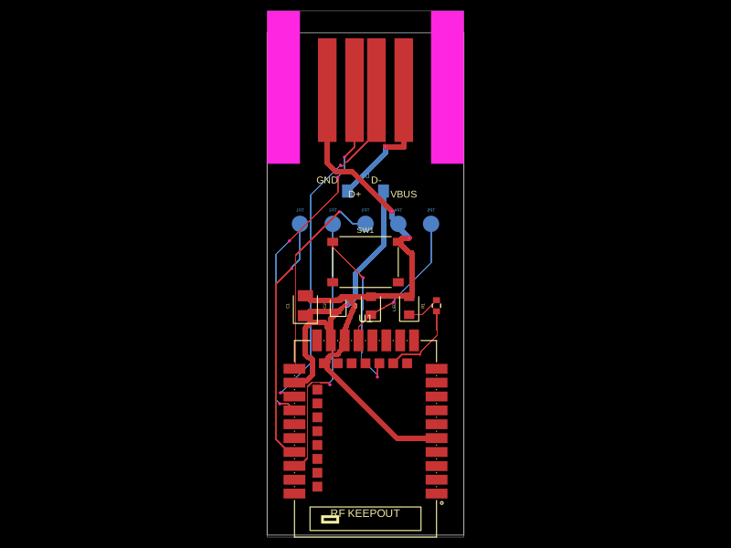 More from this authorpixalynx/keyboardThis code defines the physical layout and key components of a USB-C dongle featuring an nRF52840 microcontroller with antenna, USB-A connector, status LED, pair button, firmware debug test points, and associated passive components and interface connectors.
 Similar packagegokul/usb-hub-boardA 4-layer 100×66 mm USB 2.0 hub board with a USB‑C upstream port, four protected downstream USB‑C/USB‑A ports, an integrated SD card reader, USB hub controllers, 3.3 V regulation, ESD protection, current-limited power switches, crystal oscillators, and filtering/passive components.
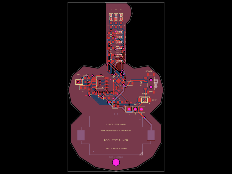 Discover something newgokul/acoustic-guitar-tunerThis code defines the physical pin configuration and footprint layouts for the ATtiny1616 microcontroller and a matching tactile switch component, including their key hardware connection points, dimensions, and 3D models.