pixalynx/usb3-hub-10g
A USB 3.2 Gen 2 six-port hub board with USB-C PD power input, regulated 5 V/3.3 V/1.15 V rails, one upstream and four protected downstream USB-A/USB-C ports, SuperSpeed muxes, ESD protection, and controlled port power.
- Version
- 0.0.1
- License
- unset
- Stars
- 0
blocks/Hub.tsx
import { pcb } from "../lib/place"
import { Fragment } from "react"
import { Usb7206c, USB7206C_VCORE, USB7206C_VDD33 } from "../parts/Usb7206c"
import { Crystal25M } from "../parts/Connectors"
import { R, C } from "../lib/passives"
import { HUB, sch, onSheet } from "../lib/layout"
import { Note, Frame } from "../lib/sch"

/** USB7206C core: supplies, straps, clock, reset and the unused-function terminations of DS00003850F Table 3-1 /
 * 3-6 and checklist DS00003336C. Port map: DN1/DN2 = USB-A (BC1.2 via CFG_BC_EN), DN3/DN4 = USB-C through the
 * HD3SS3220s, DN5/DN6 disabled by tying both USB 2.0 data pins to 3.3 V (PRT_DIS straps). */
const h = (dx: number, dy: number) => ({ x: HUB.x + dx, y: HUB.y + dy })

/** Pins that need only a weak pull-down when their function is unused (Table 3-6 "If unused"), plus the
 * disabled port-5 SuperSpeed receiver (Table 3-1: RX weak pull-down, TX left open). */
const WEAK_PD = [
  "SPI_CLK", "SPI_D1", "SPI_D2", "SPI_D3", "MSTR_I2C_CLK", "MSTR_I2C_DATA", "SLV_I2C_CLK", "SLV_I2C_DATA", "MIC_DET",
  "I2S_SDI", "I2S_SDO", "I2S_SCK", "I2S_LRCK", "I2S_MCLK", "GPIO93", "DN5_RXP", "DN5_RXN",
] as const

/** VCORE pins that sit between two SuperSpeed pairs get an 0201 decoupler that fits the gap between the pairs. */
/** VCORE leads boxed in by SuperSpeed pairs on both sides: no decoupler fits. They take an inward via under the chip to
 * the bottom-layer V1V15 pour (scripts/mesh.py), which the other six VCORE decouplers and the bulk caps serve. */
const NO_CAP = new Set(["VCORE_31", "VCORE_38", "VCORE_93"])
const STRAPS = ["CFG_STRAP1", "CFG_STRAP2", "CFG_STRAP3", "CFG_NON_REM", "CFG_BC_EN", "RBIAS"] as const
/** Schematic grids: strap / test / pull-down resistors in rows left of U1, decoupling banks above it. */
const grid = (row: number, col: number): [number, number] => [-5.0 - col * 1.25, [3.0, -0.4, -4.6, -7.8, -11.0][row]]
const VCORE_CAPS = ["C101", "C102", "C103", "C106", "C107", "C108", "C120", "C121"]
/** Decoupling banks: the placement check wants every cap of a rail on this sheet within 4 units of the others, so
 * V1V15 is 4 x 2 (1.3 x 2.6 pitch) and V3V3 3 x 3 (1.3 x 2.0 pitch). */
const bank = (rail: "V1V15" | "V3V3", k: number) =>
  rail === "V1V15" ? sch("HUB", -5.9 + (k % 4) * 1.3, 7.6 + Math.floor(k / 4) * 2.6) : sch("HUB", 1.2 + (k % 3) * 1.3, 7.6 + Math.floor(k / 3) * 2.0)
const xy = (p: { sx: number; sy: number; sec: string }) => ({ schX: p.sx, schY: p.sy, schSectionName: p.sec, ...onSheet(p.sec) })
const IN_LANE = new Set(["VCORE_9", "VCORE_18", "VCORE_31", "VCORE_38", "VCORE_85", "VCORE_93", "VDD33_88", "VDD33_62"])   // 62: 0201 so TEST1 can leave beside it

export const Hub = () => (
  <>
    <Usb7206c name="U1" {...pcb("U1", { x: HUB.x, y: HUB.y })} schX={0} schY={0} schSectionName="HUB" {...onSheet("HUB")} />
    {USB7206C_VCORE.map((p) => <trace key={p} from={`U1.${p}`} to="net.V1V15" />)}
    {USB7206C_VDD33.map((p) => <trace key={p} from={`U1.${p}`} to="net.V3V3" />)}
    <trace from="U1.VSS" to="net.GND" />

    {/* 0.1 uF at every supply pin (checklist 2.x) plus bulk on each rail */}
    {USB7206C_VCORE.map((p, i) => NO_CAP.has(p) ? null : <C key={p} name={`C${101 + i}`} v="100nF" fp={IN_LANE.has(p) ? "0201lane" : "0402"} a="V1V15" b="GND" {...h(-6.5 + i * 1.6, 8)} {...bank("V1V15", VCORE_CAPS.indexOf(`C${101 + i}`))} />)}
    {USB7206C_VDD33.map((p, i) => <C key={p} name={`C${111 + i}`} v="100nF" fp={IN_LANE.has(p) ? "0201lane" : "0402"} a="V3V3" b="GND" {...h(-6.5 + i * 1.6, -8)} {...bank("V3V3", i)} />)}
    <C name="C120" v="22uF" fp="0805" a="V1V15" b="GND" {...h(8.5, 4)} {...bank("V1V15", 6)} />
    <C name="C121" v="22uF" fp="0805" a="V1V15" b="GND" {...h(8.5, 6)} {...bank("V1V15", 7)} />
    <C name="C122" v="10uF" fp="0603" a="V3V3" b="GND" {...h(8.5, -4)} {...bank("V3V3", 8)} />
    <Note x={-6.3} y={13.3} lines={["VCORE 1.15 V decoupling: 100 nF per VCORE pin", "(pins 31/38/93 fed through vias) + 2 x 22 uF"]} />
    <Note x={0.8} y={13.3} lines={["VDD33 3.3 V decoupling: 100 nF per VDD33 pin", "+ 10 uF bulk"]} />

    {/* Configuration straps (Table 3-2..3-4): configuration 3, all ports removable, BC1.2 on ports 1-2 */}
    {/* strap, test and pull-down nets carry the hub pin's name, so the schematic can label them */}
    {[...STRAPS, "TEST1", "TEST2", "TEST3", ...WEAK_PD].map((p) => <trace key={p} from={`U1.${p}`} to={`net.${p}`} />)}
    <R name="R101" v="10k" a="CFG_STRAP1" b="GND" {...h(-9, -1)} {...sch("HUB", ...grid(0, 0))} />
    <R name="R102" v="200k" a="CFG_STRAP2" b="GND" {...h(-9, -2)} {...sch("HUB", ...grid(0, 1))} />
    <R name="R103" v="200k" a="CFG_STRAP3" b="GND" {...h(-9, -3)} {...sch("HUB", ...grid(0, 2))} />
    <trace from="U1.TESTEN" to="net.GND" />
    <R name="R104" v="10k" fp="0201lane" a="V3V3" b="TEST1" {...h(9, 1)} {...sch("HUB", ...grid(1, 0))} />
    <R name="R105" v="10k" fp="0201lane" a="V3V3" b="TEST2" {...h(9, 2)} {...sch("HUB", ...grid(1, 1))} />
    <R name="R106" v="10k" fp="0201lane" a="V3V3" b="TEST3" {...h(9, 3)} {...sch("HUB", ...grid(1, 2))} />
    <R name="R107" v="200k" a="CFG_NON_REM" b="GND" {...h(9, 5)} {...sch("HUB", ...grid(0, 3))} />
    <R name="R108" v="10k" a="CFG_BC_EN" b="GND" {...h(9, 6)} {...sch("HUB", ...grid(0, 4))} />
    <R name="R109" v="12k" a="RBIAS" b="GND" {...h(-5, 7.5)} {...sch("HUB", ...grid(0, 5))} />
    {WEAK_PD.map((p, i) => <R key={p} name={`R${120 + i}`} v="100k" fp={p.startsWith("DN5_RX") ? "0201lane" : "0402"} a={p} b="GND" {...h(-9 + (i % 9) * 1.2, -10 - Math.floor(i / 9) * 1.2)} {...sch("HUB", ...grid(2 + Math.floor(i / 6), i % 6))} />)}
    <Note x={-12.1} y={5.3} lines={["Configuration straps (DS00003850F Tables 3-2..3-4): configuration 3,", "all ports removable, BC1.2 charging on ports 1-2; RBIAS 12 k 1 %"]} />
    <Note x={-12.1} y={-2.05} lines={["Unused functions (SPI, I2C, I2S, MIC_DET, GPIO93) and the disabled", "port-5 SuperSpeed receiver: 100 k pull-downs (Table 3-6)"]} />
    {["DN5_DP", "DN5_DM", "DN6_DP", "DN6_DM"].map((p) => <trace key={p} from={`U1.${p}`} to="net.V3V3" />)}

    {/* 25 MHz crystal, 12 pF load: 18 pF each side (+ ~3 pF pin + ~2 pF stray) */}
    <Crystal25M name="Y1" {...pcb("Y1", { x: HUB.x - 3, y: HUB.y + 9.5 })} {...xy(sch("HUB", 0, -8.6))} />
    <Note x={3.6} y={-8.0} lines={["Y1 25 MHz crystal, 12 pF load", "C123/C124 18 pF each side", "(+ ~3 pF pin, ~2 pF stray)"]} />
    <trace from="Y1.OSC1" to="net.XTALI" /><trace from="U1.XTALI" to="net.XTALI" />
    <trace from="Y1.OSC2" to="net.XTALO" /><trace from="U1.XTALO" to="net.XTALO" />
    <trace from="Y1.GND2" to="net.GND" /><trace from="Y1.GND4" to="net.GND" />
    <C name="C123" v="18pF" a="XTALI" b="GND" {...h(-5.5, 11)} {...sch("HUB", -2.6, -8.8)} />
    <C name="C124" v="18pF" a="XTALO" b="GND" {...h(-0.5, 11)} {...sch("HUB", 2.6, -8.8)} />

    {/* Reset from the core regulator's power-good (blocks/Rails.tsx); upstream VBUS detect divider */}
    <trace from="U1.RESET_N" to="net.HUB_RESET_N" />
    <trace from="U1.VBUS_DET" to="net.HUB_VBUS_DET" />
    {/* divider drawn as a stack: R110 stands on R111, the junction is HUB_VBUS_DET */}
    <R name="R110" v="100k" a="VBUS_HOST" b="HUB_VBUS_DET" {...h(-9, 4)} {...sch("HUB", -10.4, 0.1)} />
    <R name="R111" v="120k" a="HUB_VBUS_DET" b="GND" {...h(-9, 5)} {...sch("HUB", -10.4, -0.5)} />

    {/* Port nets */}
    {(["UP", "DN1", "DN2", "DN3", "DN4"] as const).flatMap((p) =>
      ["DP", "DM", "RXP", "RXN"].map((s) => <trace key={`${p}${s}`} from={`U1.${p}_${s}`} to={`net.${p}_${s}`} />),
    )}
    {/* Hub transmitters get their 100 nF AC-coupling caps here (0201, next to the pins) */}
    {(["UP", "DN1", "DN2", "DN3", "DN4"] as const).flatMap((p, k) =>
      (["TXP", "TXN"] as const).map((s, j) => (
        <Fragment key={`${p}${s}`}>
          <trace from={`U1.${p}_${s}`} to={`net.${p}_${s}_HUB`} />
          <C name={`C${130 + k * 2 + j}`} v="100nF" fp="0201" horiz a={`${p}_${s}_HUB`} b={`${p}_${s}`} {...h(-8 + k * 3 + j, -12.5)} {...sch("HUB", 5.6, 4.5 - (k * 2 + j))} />
        </Fragment>
      )),
    )}
    {[1, 2, 3, 4].map((n) => <trace key={`p${n}`} from={`U1.PRT_CTL${n}`} to={`net.PRT_CTL${n}`} />)}
    <Note x={4.2} y={5.9} lines={["SuperSpeed TX AC coupling, 100 nF 0201"]} />

    <Note x={-1.5} y={-5.6} lines={[
      "U1 USB7206C: USB 3.2 Gen 2 (10 Gbps) 6-port hub, ports 1-4 used",
      "VDD33 3.0-3.6 V, VCORE 1.09-1.21 V (1.15 V nom.); typ. ~1.1 A",
      "VCORE + 75 mA VDD33 with upstream + 4 SS ports (~1.5 W)",
    ]} />
    <Frame x0={-12.4} y0={-12.6} x1={7.9} y1={13.7} title="USB 3.2 GEN 2 HUB" />
  </>
)
Related Packages
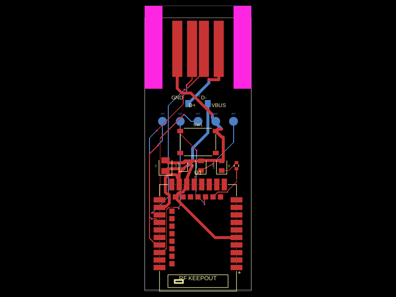 More from this authorpixalynx/keyboardThis code defines the physical layout and key components of a USB-C dongle featuring an nRF52840 microcontroller with antenna, USB-A connector, status LED, pair button, firmware debug test points, and associated passive components and interface connectors.
 Similar packagegokul/usb-hub-boardA 4-layer 100×66 mm USB 2.0 hub board with a USB‑C upstream port, four protected downstream USB‑C/USB‑A ports, an integrated SD card reader, USB hub controllers, 3.3 V regulation, ESD protection, current-limited power switches, crystal oscillators, and filtering/passive components.
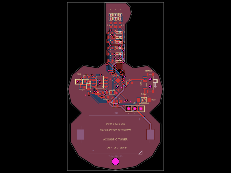 Discover something newgokul/acoustic-guitar-tunerThis code defines the physical pin configuration and footprint layouts for the ATtiny1616 microcontroller and a matching tactile switch component, including their key hardware connection points, dimensions, and 3D models.