pixalynx/pixal-nfc-card
This code defines React components representing specific electronic hardware components—namely, a 100-ohm SMD resistor, a surface-mount LED, and a chip with labeled pins—each modeled with detailed footprints, 3D CAD models, and manufacturer part information for PCB design.
- Version
- 1.1.0
- License
- unset
- Stars
- 0
scripts/audit-manufacturing.py
import json, math, re, sys
from pathlib import Path
from shapely.geometry import Point, LineString, Polygon, box
from shapely.ops import unary_union
from PIL import Image, ImageDraw

ROOT=Path(sys.argv[1])
d=json.loads((ROOT/'release.circuit.json').read_text())
board=next(e for e in d if e['type']=='pcb_board')
outline=Polygon([(p['x'],p['y']) for p in board['outline']])
ports={e['pcb_port_id']:e for e in d if e['type']=='pcb_port'}
sp={e['source_port_id']:e for e in d if e['type']=='source_port'}
comps={e['source_component_id']:e['name'] for e in d if e['type']=='source_component'}
def pn(pid):
 p=sp[ports[pid]['source_port_id']]
 return comps[p['source_component_id']]+'.'+p['name']
def net(pid):
 p=sp[ports[pid]['source_port_id']]
 return p.get('subcircuit_connectivity_map_key',p['source_port_id'])
def rect(e): return box(e['x']-e['width']/2,e['y']-e['height']/2,e['x']+e['width']/2,e['y']+e['height']/2)
copper=[]
for e in d:
 if e['type']=='pcb_smtpad': copper.append((pn(e['pcb_port_id']),e['layer'],net(e['pcb_port_id']),rect(e)))
 if e['type']=='pcb_plated_hole':
  for ly in ['top','bottom']:copper.append((pn(e['pcb_port_id']),ly,net(e['pcb_port_id']),Point(e['x'],e['y']).buffer(e['outer_diameter']/2)))
 if e['type']=='pcb_trace' and e.get('source_trace_id'):
  ps=e['route'];ls=LineString([(p['x'],p['y']) for p in ps]);copper.append((e['pcb_trace_id'],ps[0]['layer'],net(ps[0]['start_pcb_port_id']),ls.buffer(ps[0]['width']/2)))
gaps=[]
for i,a in enumerate(copper):
 for b in copper[i+1:]:
  if a[1]==b[1] and a[2]!=b[2]:gaps.append((a[3].distance(b[3]),a[0],b[0]))
print('Smallest top copper clearances (distinct source nets):',sorted(gaps)[:8])
coil=next(e for e in d if e['type']=='pcb_trace' and e.get('pcb_component_id'))
pts=[(p['x'],p['y']) for p in coil['route']];segs=[LineString([a,b]) for a,b in zip(pts,pts[1:])]
cgaps=[(a.distance(b)-.45,i,j) for i,a in enumerate(segs) for j,b in enumerate(segs) if j>=i+2]
print('Independent minimum turn clearance:',min(cgaps))
print('Coil centerline length mm:',sum(s.length for s in segs))
print('Full-outline coil edge clearance mm:',outline.boundary.distance(LineString(pts))-.225)
print('Estimated coil DC resistance ohm at 35um copper:',1.724e-8*sum(s.length for s in segs)*.001/(.00045*.000035))
# Independent square-spiral current-sheet approximation: use mean of x/y outer and inner dimensions.
dout=(46.45+44.45)/2*.001;din=(38.35+36.35)/2*.001;avg=(dout+din)/2;rho=(dout-din)/(dout+din)
L=4*math.pi*1e-7*25*avg*1.27/2*(math.log(2.07/rho)+.18*rho+.13*rho*rho)
print('Approximate square current-sheet cross-check uH:',L*1e6)
for c in [47.5,50,52.5,55,60]: print('f0 MHz, 2.536uH, C pF',c,1/(2*math.pi*math.sqrt(2.536e-6*c*1e-12))/1e6)
print('Capacitance pF at 13.56MHz, 2.536uH:',1/(4*math.pi**2*13.56e6**2*2.536e-6)*1e12)
# Parse the subset of Gerber used by this export: C/R apertures, linear strokes and flashes.
def gerber(name):
 text=(ROOT/'gerbers'/name).read_text();assert '%FSLAX46Y46*%' in text and '%MOMM*%' in text, 'Unsupported Gerber coordinate format';assert all(t in ['C','R'] for t in re.findall(r'%ADD\d+([A-Za-z_][A-Za-z0-9_]*)[,\*]',text)), 'Unsupported aperture';aps={int(i):(typ,[float(x) for x in val.split('X')]) for i,typ,val in re.findall(r'%ADD(\d+)([CR]),([0-9.X]+)\*%',text)}
 body=text.split('G04 aperture END LIST*')[-1];x=y=0.;ap=None;out=[]
 for line in body.splitlines():
  m=re.fullmatch(r'D(\d+)\*',line)
  if m:ap=int(m[1]);continue
  m=re.fullmatch(r'X(-?\d+)Y(-?\d+)D(0[123])\*',line)
  if not m:continue
  xx,yy=int(m[1])*1e-6,int(m[2])*1e-6;op=m[3];typ,sz=aps[ap]
  if op=='03':out.append((Point(xx,yy).buffer(sz[0]/2) if typ=='C' else box(xx-sz[0]/2,yy-sz[1]/2,xx+sz[0]/2,yy+sz[1]/2),sz[0]))
  if op=='01':
   assert typ=='C'
   out.append((LineString([(x,y),(xx,yy)]).buffer(sz[0]/2),sz[0]))
  x,y=xx,yy
 return out
ge={n:gerber(n+'.gbr') for n in ['F_Cu','B_Cu','F_Mask','B_Mask','F_Paste','B_Paste','F_SilkScreen','Edge_Cuts']}
for n,shapes in ge.items():
 u=unary_union([g for g,w in shapes]);print(n,'primitives',len(shapes),'bounds',u.bounds,'islands',len(u.geoms) if hasattr(u,'geoms') else 1)
mask=unary_union([g for g,w in ge['F_Mask']]);silk=unary_union([g for g,w in ge['F_SilkScreen']]);print('Silkscreen-mask minimum gap',mask.distance(silk),'intersection area',mask.intersection(silk).area)
print('Silkscreen line widths:',sorted(set(w for g,w in ge['F_SilkScreen'])))
for p in [e for e in d if e['type']=='pcb_smtpad']:
 print('Silk clearance',pn(p['pcb_port_id']),round(rect(p).distance(silk),4))
# Render unmodified Gerber primitives for visual inspection.
def render(name,bounds,scale,layers):
 xmin,ymin,xmax,ymax=bounds;im=Image.new('RGB',(int((xmax-xmin)*scale),int((ymax-ymin)*scale)), '#171b23');dr=ImageDraw.Draw(im)
 def xy(x,y):return ((x-xmin)*scale,(ymax-y)*scale)
 for layer,color in layers:
  for shape,w in ge[layer]:
   gs=list(shape.geoms) if hasattr(shape,'geoms') else [shape]
   for g in gs:dr.polygon([xy(x,y) for x,y in g.exterior.coords],fill=color)
 im.save(ROOT/name)
render('gerber-detail.png',(1,-5,15.5,5),140,[('B_Cu','#284f87'),('F_Cu','#c9833e'),('F_SilkScreen','#eeeeaf'),('F_Paste','#e16791')])
render('gerber-board.png',(-44,-28,44,28),22,[('Edge_Cuts','#aaaaaa'),('B_Cu','#376ba9'),('F_Cu','#d99b42'),('F_SilkScreen','#ffffbb')])

# Independent release gates against actual geometry and exported Gerbers.
def require(ok,msg):
 print(('PASS ' if ok else 'FAIL ')+msg)
 assert ok,msg
require(board['num_layers']==2 and abs(board['thickness']-.6)<1e-6,'two layers, 0.6 mm board')
require(abs(outline.bounds[2]-outline.bounds[0]-85.6)<1e-6 and abs(outline.bounds[3]-outline.bounds[1]-54)<1e-6,'85.6 x 54 mm outline')
require(min(g[0] for g in gaps) >= .15,'unrelated copper clearance >=0.15 mm')
require(min(g[0] for g in cgaps) >= .44999,'every nonadjacent antenna turn separated')
require(outline.boundary.distance(LineString(pts))-.225 >= 3.27,'rounded-outline antenna clearance')
require(len(ge['F_Paste'])==5 and len(ge['B_Paste'])==0,'five top paste apertures; zero bottom paste')
require(mask.distance(silk) >= .15-1e-5,'silkscreen to solder mask openings >=0.15 mm')
require(min(w for g,w in ge['F_SilkScreen'])>=.15-1e-6,'minimum silkscreen stroke 0.15 mm')
require(outline.buffer(-.2).covers(silk),'all silk at least 0.2 mm inside outline')
require(all(outline.buffer(-.2).covers(g) for label,ly,n,g in copper),'all pads and feeds inside routed edge clearance')
keepouts=[e for e in d if e['type']=='pcb_keepout']
require(len(keepouts)==1 and set(keepouts[0]['layers'])=={'top','bottom'},'explicit both-layer RF keepout')
require(set(comps.values())=={'U1','L1'},'only IC and printed antenna exist')
require(len([e for e in d if e['type']=='pcb_trace'])==3,'exactly two feeds and one antenna trace')
require(not [e for e in d if e['type'] in ['pcb_via','pcb_copper_pour','pcb_copper_polygon']], 'no extra vias or copper fill')
# Reject any added top copper within RF zone, except the two documented feeds/terminals.
zone=box(-40.8,-23.5,8.2,23.5)
for label,ly,n,g in copper:
 if ly=='top' and g.intersects(zone):
  require(label.startswith('L1.') or label in [e['pcb_trace_id'] for e in d if e['type']=='pcb_trace' and e.get('source_trace_id')],'RF keepout contains only allowed feed/terminal copper')
# Prove that export did not omit or add copper and that the coil is a single island.
for ly,gn in [('top','F_Cu'),('bottom','B_Cu')]:
 expected=unary_union([g for label,l,n,g in copper if l==ly]+([LineString(pts).buffer(.225)] if ly=='bottom' else []))
 actual=unary_union([g for g,w in ge[gn]])
 delta=expected.symmetric_difference(actual).area
 require(delta<.001,f'{gn} agrees with source copper (difference {delta:.8f} mm2)')
 require(actual.geom_type=='Polygon' if ly=='bottom' else len(actual.geoms)==5,'bottom continuous coil / top two feeds plus three isolated NC pads')
for p in [e for e in d if e['type']=='pcb_smtpad']:
 matches=[g for g,w in ge['F_Paste'] if g.centroid.distance(Point(p['x'],p['y']))<1e-4]
 require(len(matches)==1 and matches[0].symmetric_difference(rect(p)).area<1e-5,'IC paste 1:1 with manufacturer copper land')
# Geometric detector regression: a rogue plane inside the loop must fail the export-equivalence check.
base=unary_union([g for g,w in ge['B_Cu']])
require(base.union(box(-20,-2,-10,2)).symmetric_difference(base).area>1,'self-test detects added copper inside loop')
print('Manufacturing geometry audit passed; physical RF and supplier process acceptance remain external gates.')

# Drill tooling and exported mask coverage are release-critical, too.
drill=(ROOT/'gerbers/drill-L1-L2.drl').read_text()
require('METRIC' in drill and 'T10C0.300000' in drill,'metric 0.30 mm plated drill')
require(set(re.findall(r'X([-0-9.]+)Y([-0-9.]+)',drill))=={('6.7000','-3.0000'),('2.2000','3.0000')},'exactly the two antenna terminal drill positions')
require(len(re.findall(r'^X',drill,re.M))==2,'exactly two drills')
require(len(ge['F_Mask'])==7 and len(ge['B_Mask'])==2,'only IC and terminals are exposed through mask')
k=keepouts[0]
require(abs(k['center']['x']+16.3)<1e-5 and abs(k['center']['y'])<1e-5 and k['width']==49 and k['height']==47,'RF keepout dimensions unchanged')
Related Packages
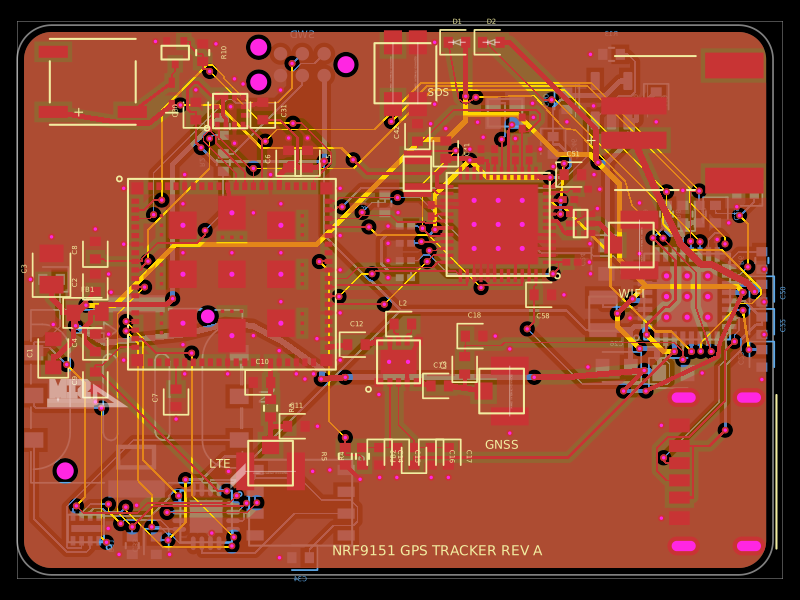 More from this authorpixalynx/nrf9151-gps-trackerA compact 44×32 mm, 4-layer nRF9151 LTE-M/NB-IoT/GNSS tracker PCB with nPM1300 LiPo/USB-C power, nano-SIM/eSIM switching, nRF7002 Wi‑Fi scanning, accelerometer, antennas, buzzer, LEDs, SOS button, and SWD/debug connectors.
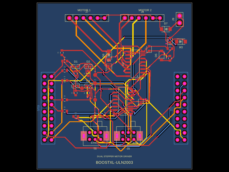 Similar packageabse/boostxl-uln2003This code defines a React component that models a through-hole or surface-mount LED with specified pin labels, footprint, silkscreen, and 3D CAD model for PCB layout.
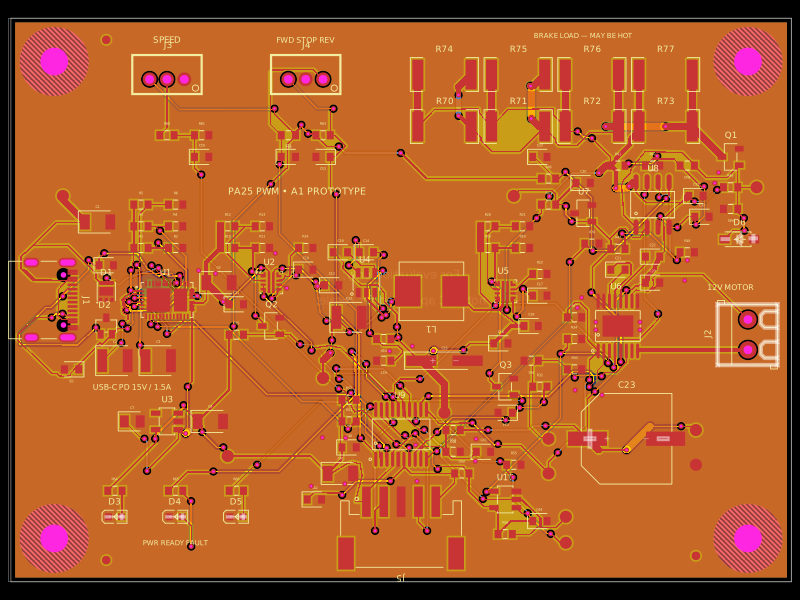 Discover something newAnasSarkiz/usb-c-pwm-pa25A component library defining an AO3400A N-channel MOSFET, 47 µF polarized capacitor, 3-pin through-hole connector, and 9.1 V Zener diode with PCB footprints and 3D CAD models.