pixalynx/pixal-nfc-card
This code defines React components representing specific electronic hardware components—namely, a 100-ohm SMD resistor, a surface-mount LED, and a chip with labeled pins—each modeled with detailed footprints, 3D CAD models, and manufacturer part information for PCB design.
- Version
- 1.1.0
- License
- unset
- Stars
- 0
fabrication/rev-b/RF-VALIDATION.md
PCB

Schematic

# Revision B RF and functional qualification

No measured resonance, Q, range, bend life or assembled yield has been claimed. The direct differential antenna plus the ST25TN01K internal nominal 50 pF capacitance is a credible passive tag topology. Additional generic reader matching/filter components are not required. No LED load or experimental shunt capacitance is fitted.

The winding-only estimate is 2.536 µH, nominal resonance 14.13 MHz with 50 pF; 47.5–52.5 pF gives 14.50–13.79 MHz before feed inductance and parasitic capacitance. Geometry alone cannot establish assembled tuning or Q. Retain revision B as the baseline; adjust geometry from measurements, not an assumed benefit from a user's hand.

## Prototype plan and proposed acceptance criteria

Build at least 10 assembled cards from the same material/process and retain 2 unpopulated cards from that lot for coil characterization. This is initial engineering screening, not statistical production qualification. Record board lot, IC lot, finish, copper thickness, actual board thickness, covering/adhesive and instrument settings.

1. Inspect winding and U1 joints. Verify bare-coil continuity with four-wire resistance where practical (~0.9 Ω winding-only estimate at 35 µm Cu, plus feeds). AC0-to-AC1 DC continuity is intended. NC pins must remain isolated. Check for adjacent-turn bridges optically: continuity alone cannot detect them.
2. Measure unpopulated antenna impedance near 13.56 MHz with a calibrated/de-embedded low-parasitic differential fixture. Determine L, series R and self-resonance; record fixture uncertainty. Do not attach an ordinary scope probe directly across the assembled tag and mistake its loading for native resonance.
3. Follow ST AN2866 contactless loop/VNA method: sweep 10–20 MHz initially, refine around resonance, begin at low drive (e.g. -10 dBm at VNA port), repeat lower/higher levels within safe fixture conditions. Change probe spacing and orientation to establish weak coupling without splitting/strongly loading the resonance. Port power is not voltage at the IC. Record raw S11/phase and setup pictures. Do not infer tag Q from a strongly coupled probe's bandwidth.
4. Measure bare assembled cards and finished nonmetallic covered cards, then repeat with normal hand grip and intended wallet context. Initial ST25TN design target is 13.6–14.0 MHz in the defined final stack under weak coupling. Record drive and environmental shifts; this target is a design criterion, not a compliance certificate or universal phone optimum.
5. If high, increase loop inductance/area or evaluate a small high-Q C0G shunt capacitance on an engineering rework sample; if low, reduce inductance/parasitics. Any capacitor needs a reviewed footprint/routing revision. Recalculate and regenerate all files, remeasure, and keep RF loading low. Do not blindly add the idealized ~4.3 pF calculated for 13.56 MHz.
6. Program a short NDEF URI record using a compatible Type 2 tag tool. The final personal URL has not been specified; use an explicitly temporary test URI and verify readback. Do not set permanent lock/password bits during engineering tests. Test write/read and power-loss recovery per ST guidance; erase the temporary payload before final personalization.
7. Proposed initial functional gate: at least 3 NFC phone models covering iOS and Android, 10 taps per phone per face at 0, 5 and 10 mm nonconductive stand-off, with the phone antenna centred over the TAP zone. Record cases, orientation and OS/app. Require 10/10 successful reads within 2 seconds at 0 and 5 mm on every tested phone/face. Characterize 10 mm and maximum stable range; treat repeatable failures at required positions as a redesign trigger. Repeat with final covering and normal grip. These are project targets, not promises of tested performance.
8. Repeat visual, resonance and phone tests after the handling trials in MECHANICAL.md. Retain baseline traces and a results table per sample. Release production only after deviations are resolved and the desired use-case range is accepted.

Reference: [ST AN2866 Rev 6, sections 4–6](https://www.st.com/resource/en/application_note/an2866-how-to-design-a-1356-mhz-customized-antenna-for-st25-nfc--rfid-tags-stmicroelectronics.pdf). ST recommends 13.6–14.0 MHz for ST25TN and explicitly requires final-material/environment effects to be considered.
Related Packages
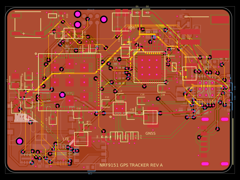 More from this authorpixalynx/nrf9151-gps-trackerA compact 44×32 mm, 4-layer nRF9151 LTE-M/NB-IoT/GNSS tracker PCB with nPM1300 LiPo/USB-C power, nano-SIM/eSIM switching, nRF7002 Wi‑Fi scanning, accelerometer, antennas, buzzer, LEDs, SOS button, and SWD/debug connectors.
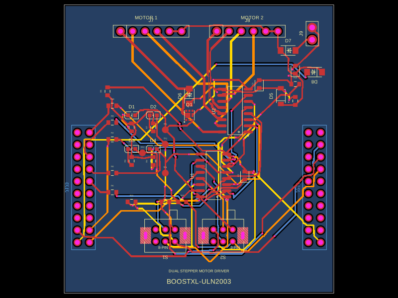 Similar packageabse/boostxl-uln2003This code defines a React component that models a through-hole or surface-mount LED with specified pin labels, footprint, silkscreen, and 3D CAD model for PCB layout.
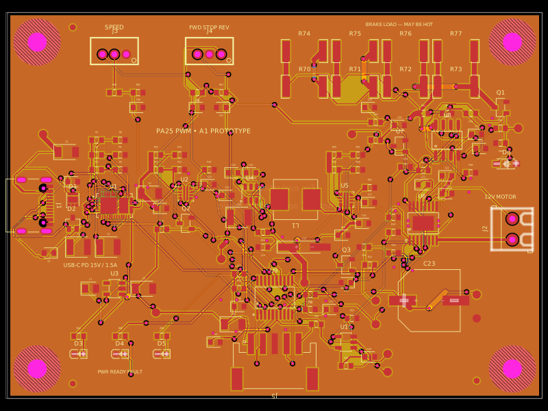 Discover something newAnasSarkiz/usb-c-pwm-pa25A component library defining an AO3400A N-channel MOSFET, 47 µF polarized capacitor, 3-pin through-hole connector, and 9.1 V Zener diode with PCB footprints and 3D CAD models.